A 1-V 10-bit 16.83-fJ/Conversion-step Mixed Current Mode SAR ADC for WSN

Author: Dipak S. Marathe, Uday P. Khot
Journal: International Journal of Image, Graphics and Signal Processing @ijigsp
Article in issue: 11 vol.11, 2019.
Free access
This paper proposes a 10-bit mixed current mode low power SAR ADC for sensor node application. The different entities of a successive approximation register (SAR) analog-to-digital converter (ADC) circuit has a hybrid or mixed mode approach i.e.,voltage mode regenerative comparator; mixed SAR logic; and current mode digital-to-analog converter (DAC). The performance limitation of speed and the kick-back noise of a dynamic comparator is resolved using duty cycle controlled regenerative comparator. A mixed mode logic of a SAR is partitioning the design into synchronous ring counter and asynchronous output register. The data shifting of a ring counter is with the common clock tick while the output register exchanged it asynchronously using handshake signals, resulting in a low power SAR. The current mode switching function in a DAC to reduce asynchronous switching effect resulting in a low energy conversion per step. In overall, the proposed mixed SAR ADC consumes a 41.6 power and achieves an SFDR 69.3 dB at 10 MS/sec and 1 V supply voltage. It is designed and simulated in the 0.18 m TSMC CMOS process.
Successive approximation register (SAR), mixed-mode, current-mode, regenerative -comparator, analog-to-digital-converter (ADC), digital-to-analog converter (DAC)
Short address: https://sciup.org/15017050
IDR: 15017050 | DOI: 10.5815/ijigsp.2019.11.06
Text of the scientific article A 1-V 10-bit 16.83-fJ/Conversion-step Mixed Current Mode SAR ADC for WSN
Published Online November 2019 in MECS
There is a significant thrust towards low power design methodologies for high resolution and high speed applications. The growing demand for small, high speed battery operated devices is increasing. A smaller feature size CMOS technologies can reduce power consumption; however, other non-idealities and process variations will significantly affect the overall performance of the devices. One such application where high speed, low power and high resolution are required is analog-to-digital converters (ADCs) used in wireless sensor node (WSN). There are numerous tiny devices which are making use of these ADCs. All the laptops and mobile phones have in build wireless personal area network (WPAN), and this is where low power, high speed and high resolution ADC is highly required. Advancing from 3G cellular networks into 4G and 5G is also another sign of the increasing demand for high speed and low power ADCs.
Section II illustrates the conventional SAR ADC. In section III brief idea about hybrid or mixed mode approach. In section IV, V, and VI discuss circuit implementation details of SAR ADC. Section VII describes the proposed mixed mode SAR type ADC. The simulation results discussed in Section VIII. Section IX and X provides a future work and conclusion.
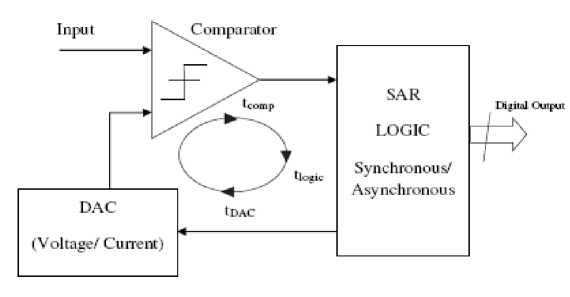
Fig. 1. Conventional SAR ADC architecture [1, Modified].
-
II. A SAR ADC
The typical architecture [1] of a SAR type ADC is representing in Fig. 1., have a comparator, SAR logic either synchronous, asynchronous or mixed mode and current or voltage mode type DAC. The comparator compares the analog input with the reference signal coming from DAC. The comparator output generates square pulses. A SAR logic shifts and counts these pulses. The DAC is converting back digital pulses to an analog reference signal of a comparator. The worst case time for one-bit conversion shown in Eq. (1), and is defined as the summation of comparator time, SAR logic, and conversion time of a DAC.
Table 1. Pros and cons of a different combination of SAR ADC
|
Comparator |
SAR |
DAC |
||||
|
Type |
Regenrative |
Dynamic |
Synchronous |
Mixed |
Voltage mode |
Current mode |
|
Pros |
High speed, Highly sensitive |
Low power |
Fast |
Low power |
Low freqeuncy |
High frequency |
|
Cons |
High power |
Low sensitive, slow |
High power |
Slow |
Slow |
Initial cuurent is high |
Table 2. Types SAR based ADC
|
Type |
Comparator |
SAR |
DAC |
|
I |
Voltage Mode |
Mixed |
Current Mode |
|
II |
Voltage Mode |
Syn. |
Current Mode |
|
III |
Voltage Mode |
Mixed |
Voltage Mode |
|
IV |
Voltage Mode |
Syn. |
Voltage Mode |
The simplified version of critical time can be found using Eq. (2).
T critical = t comp + t logic + t DAC
T critical = t mincycletime + t pd ( min ) + t DACsettle
The Eq. (1) can rewrite as Eq. (2) in terms of t is the minimum cycle time of a comparator, mincycletime , t is a logical time for conversion from SAR, and pd (min) , t is settling time of a DAC respectively.
To have an energy-limited application in wireless sensor networks with the power efficient SAR ADC can extend the product life. For such applications, ADCs are usually required to have a full range resolution (8-12 bits), 1 kS/s - 100 MS/s sampling rate, and ultra-low voltage. In [1], Asynchronous SAR logic is used. The linearity of an ADC and common-mode voltage value decreases or increases monotonically and depends on the sign of V . This fact can make the design complex and degrade linearity. In [2], a self-synchronization SAR ADC with comparator at 8- bit accuracy level technique saves power in the comparator. This technique introduces decision errors and hence there is a tradeoff between accuracy and power. In [3], a split capacitor DAC and latch comparator will add more pre-amplification stages and increase the gain of a comparator. This strategy shortens a period and reduces the power dissipation of the comparator, but the speed of an ADC is limited.
-
III. Hybrid Or Mixed Mode Approach
A 10-bit mixed current mode SAR ADC is based on the pros and cons of different entities of a SAR ADC are shown in Table 1. It uses a regenerative comparator and controlling the power using duty cycle. The mixed low power SAR logic is a combination of synchronous and asynchronous, which utilizes the advantages of both techniques. Finally, the current mode DAC makes it energy efficient. The overall performance of all these entities would benefit it from forming a hybrid SAR ADC. Based on the different combination of a SAR and DAC types of ADCs are decided and is shown in Table 2. The regenerative comparator for all kinds of ADC is voltage mode. The Type-I and Type-III are the mixed mode, i.e., synchronous plus asynchronous SAR logic with current or voltage mode DAC. The Type-II and Type-IV are combinations of synchronous SAR logic with either current or voltage mode DAC.
-
IV. Regenerative Comparator
The sensor node in the WSN will sense the physical activity with the help of different types of sensors and transducer. This physical phenomenon processed and converted into the digital form and sent it to the base station or server. The basic block of SAR ADC in a WSN is a comparator. The regenerative comparator is shown in Fig. 2., has three stages a preamplifier stage-I, preamplifier stage-II, and latch. The positive feedback latch block used for quick decision with small power and area consumption. The use of the clock pulse can significantly improve comparator performance, speed and low power dissipation with an adjustable duty cycle. The clock also eliminates the need for an output buffer which is used in the level shifting the output of the preamplifier stage -II block. The transient simulation of regenerative comparator is shown in Fig. 3.
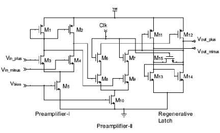
Fig. 2. Schematic View of Proposed CMOS Regenerative Comparator.
which will violate the setup ( T ) and hold time( T ). These timing parameters are interdependent and also have the non-linear behavior. That is, if hold time is high then setup time is small or vice-versa [3].
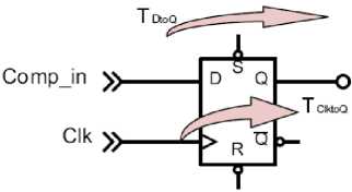
Fig. 4. Block Diagram of D Flip-Flop (SAR Logic).
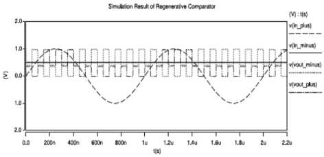
Fig. 3. Transient Simulation of the Regenerative Comparator.
A. Power control using Duty cycle
Assuming energy; E and power is a rate of change of energy flow per unit time, the peak power, and average power for one full period ( f = ) in terms of energy which are representing in Eq. (3) and Eq. (4).
P , peak
E
A t
P avg
E
T
-
(3)
-
(4)
C. Optimum Duty Cycle
The duty cycle has a direct relationship with the average power consumed by the circuit shown in Eq. (6). A comparator uses a clock signal, i.e., variation in the period of a clock varies the power. The optimum duty cycle defined as the ratio of the active or on-period to the total pulse width. The non-linear behavior of timing constraints ( T , T ) will affect power consumption. The minimum active period in our case, determined by considering the two scenarios with the worst case condition. The first scenario is ( T , T ) and
H,max S,max second is ( T , T ). This timing constraint will H,min S,min insert additional stages of a register and dissipating extra power. Therefore, to determine the appropriate timing constraints for a valid range is considered, i.e. (T , T ) [4,5] and calculated using Eq. (8). The duty cycle for a valid range is calculated using Eq. (9). The optimum timing constraints are calculated using in Eq. (10), and Eq. (11) respectively for minimum and maximum value of T , T . The optimum duty cycle is calculated using Eq. (12).
The Duty Cycle is the fractional amount of time in which the device is on during any given period is expressing in Eq. (5).
Duty - cycle ( го ) = — = avg (7)
T Ppeak
Duty - cycle ( го ) = ^ t
Thus, the duty cycle writes as concerning of average and peak power and it is representing in Eq. (6)
0 , r = TDto Q + ClktoQ + T s , r + T h , r (8)
T ror = -fr (9)
T total
P
Duty - cycle =---- (6)
P peak
T = T ,.+T ,.+T + T on, min DtoQ ClktoQ S, min H, min
B. Setup and Hold Time
The SAR logic uses a D-flip-flop structure that is shown in Fig. 4. The input to output delay ( T ) is the signal carrying time to the input of the flip-flop. Time is taken by the flip-flop to get the output when a clock pulse is applied. This is called as a clock to Q delay ( T ). A width of a clock pulse is too short or long,
T on, max
DtoQ + ClktoQ + S , max + H , max
го optimum
T on ( optimum )
T , total
Where, Ton r is an on period, and ror is a duty cycle
for a valid range. For CMOS 180 nm technology timing
parameters are T = 41 , T = 3.3 , T = 139 , and T = 53.7 respectively [4].
-
V. Mixed Mode SAR Logic
The mixed operating mode of SAR shown in Fig. 5., is a combination of synchronous and asynchronous logic, which utilizes the merits of synchronous and asynchronous logic called mixed mode SAR. The SAR can be implemented in either synchronous logic or combination of synchronous and asynchronous digital logic. A 1-bit mixed mode logic shown in Fig. 6. The simulation result of mixed mode SAR logic [6] is shown in Fig. 7. The D-latch of mixed logic is designed using multiplexer shown in Fig. 8. A mixed mode architecture uses a global clock net to partitioning the design. Each partitioned part exchanges data asynchronously using handshake signals [6]. The designing of synchronous and asynchronous 10-bit SAR is carried out using CMOS 180 nm technology. A propagation delay of flip-flop for synchronous is equal to the propagation delay of just one flip-flop because all flip-flops are triggered simultaneously by the clock. An asynchronous logic would add all flip- flops delay. The period of the clock pulse (T ) is 100 ns, and N is the number of bits. A minimum propagation delay of a flip-flop t expressed as, tpd(min)
т
C
N
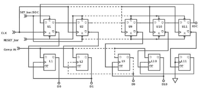
Fig. 5. Schematic View of 10-bit Mixed (Synchronous + Asynchronous) SAR.
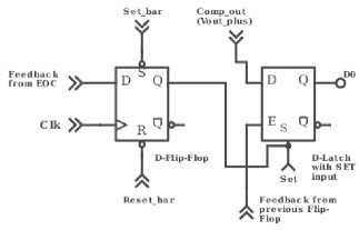
Fig. 6. Schematic View of 1-bit Mixed SAR.
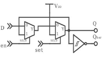
Fig. 7. Schematic View of 1-bit D-latch using Multiplexer.
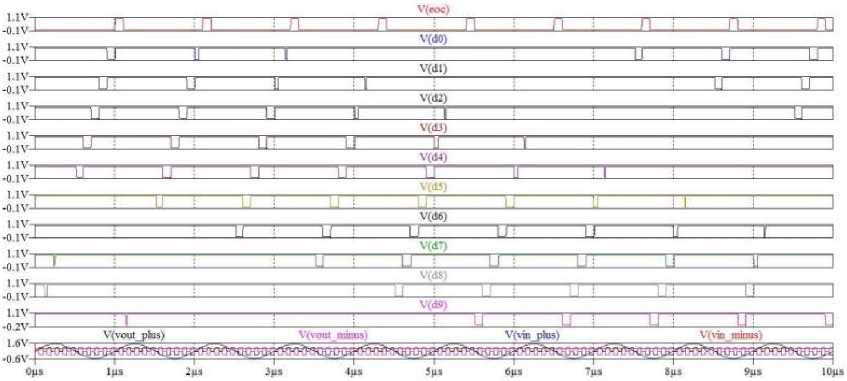
Fig.8. Simulation result of 10-bit Mixed SAR.
Current Mode DNL
-
VI. Current Mode DAC
In binary weighted type DAC, the last most significant current source is enabled and all other current sources are disabled from the output. It makes it very difficult to match the value of the previous current source and a summation of all other current sources to limit within ± 0.5 LSB. The monotonicity of the DAC cannot be guaranteed. The glitches at DAC output would increase due to an asynchronous effect of current switching and parasitic capacitance.
The thermometer coded type DAC is used to minimize the switching effect at the output. Where 2 N - 1 current sources are used. This unit cell of current references form a matrix, the size of matrices depends on the number of DAC bits. Each unit cell connected in the array driven by the thermometer decoder. For each binary value of the digital code, only one current cell is switched to the converter output and maintained other current sources off. It would minimize the asynchronous switching at a great extent.
t D A C s e < t
VFS
, N - 1
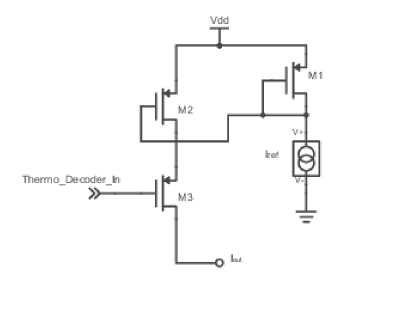
Fig. 9. Schematic View of Current Mode Switch.
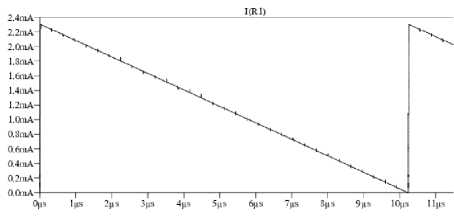
Fig. 10. Result Current mode DAC Transient Simulation.
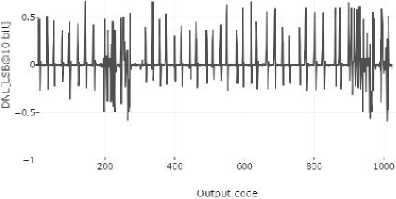
Fig. 11. 10-bit Current Mode DAC DNL.
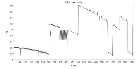
Fig.12. 10-bit Current Mode DAC INL.
I FS = f 1 1 k ( V gs - V h )2(1 + ^i f W 1 (16)
к 2 J i к L J i
Where, IFS is a full-scale current, k = ^ Cm is the CMOS process constant (ц is the mobility of holes, Cm is oxide capacitance), 1 = ^L 1 is channel
LV ds length modulation due to drain-source voltage, V is a gate to source bias, V is a threshold voltage, and | W | is an aspect ratio of it cell. All switching matrix к L J, cells were contributing a DAC full-scale current and a switching current in each cell is expressing in Eq. (15), and Eq. (16) [7].
N - S 2 m - 1 2 S - 1 2 N - S + m *2 N - S - 1
^K = I B k , m £ I u ,i + £ T k , m £ I u ,i (17)
m =1 i =2 m - 1 m =1 i =2 N - S + ( m - 1)2 N - S
The generalized binary and thermometer type DAC output equation has shown in Eq. (17). In our case, we are using thermometer type DAC. Ignoring binary part of Eq. (17) can be rewritten as Eq. (18) or Eq. (19) for thermometer type DAC [7].
Where, V are a full-scale voltage, and N is the number of bits.
I FS = £ f 1 1 k f W 1 (V gs - V ^)2(1 + ^ V ds ) (15)
i к 2 J к L J i
Thermo
I out , K
2 N - 1
K
I T k , m I I u ,i
m =1
i =1
I out , K
2 N - 1
Yk *l,
I K, m U, i m=1
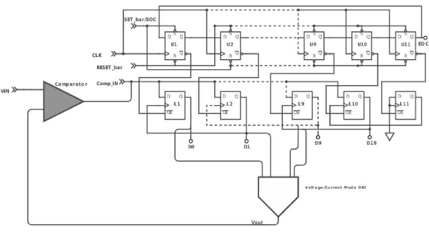
Fig. 13. Schematic View of Mixed Current mode SAR ADC.
where, N is the bit DAC resolution, S indicates the segmented bits either for the thermometer, binary or both, B binary and T thermometer code switching matrices respectively. For binary and thermometer parts, i e[1:2N -1], K e[0:2N-1], and m e[1:2N -1] . If, S = N then the Eq. (17) becomes fully thermometer DAC and is shown in Eq. (18) and Eq. (19). If, S = 0 then it becomes fully binary DAC otherwise it is segmented i.e., thermometer plus binary.
For 10-bit DAC, i e [1:1023], K e [0:1023], and m e [1:1023]. For, 5 = N, switching matrices for a thermometer DAC code (T ) can be represented as,
T2N *2 N - 1 T 1024*1023
If,
T
K , m
0 0 0. . .01
0 0 0. .0 11
0 0 0.0 1 11
. . . . . ..1
. . . . . ..1
. . . . . ..1
1 . .01111
_1 . . 1 1 1 11
-
1, m > 0
, m <0
The overall linearity of DAC can be specified in terms of integral nonlinearity (INL), i.e. deviation of actual DAC output current from the ideal straight line drawn between the two end points 0 and I . A differential nonlinarity (DNL) is a measure of the deviation of the actual DAC output current step from the ideal current step for 1 LSB.
DNL ( i ) = I ( i + 1) - I ( i )
DeviceLSB
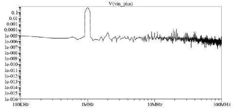
Fig. 15. Measured output FFT.
INL ( i ) =
I - ( DeviceLSB * i ) DeviceLSB
I *(2 N - 1) - I )
DeviceLSB = ( i ) (0) (23)
(2 N - 1)
Where i is the number of steps i.e., 0 to 1023. In the current mode circuit switching is carried out by controlling a current in the unit cell shown in Fig. 9. A digital logic input coming from mixed mode SAR logic [6] drives a thermometer DAC switching matrix. The transient simulation of 10-bit current mode DAC is shown in Fig. 10. The non-linearity performance analysis for differential and integral i.e DNL, INL are shown in Fig. 11 and 12.
-
VII. Proposed Mixed Current Mode SAR ADC
As the technological development in wireless networking, VLSI and the embedded system has enabled a new growth for wireless sensor networks (WSNs). Thus, WSNs becomes the first choice for a wide range of commercial and military application. The tiny and inexpensive sensors are everywhere in the intelligent infrastructure or even in the animals to sense various physical activities of interest, such as monitoring bio-medical, environmental conditions, smart vehicles, reporting emergency conditions, or detecting natural calamity and industrial automation [2,8].
A power dissipation (Pdiss) and energy consumption are fundamental important parameters in a circuit employed with the application of wireless sensor networks (WSNs). The restriction on the amount of a power budget or source of energy in an Ultra-Low-Power (ULP) application has the most crucial design design issue [9]. The utmost care should take for allocating a power budget to a circuit as per WSN applications.
-
VIII. Simulation Result
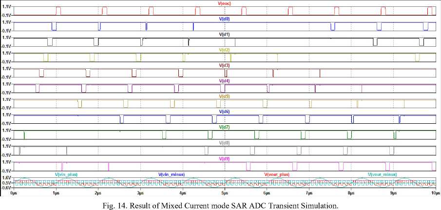
The proposed SAR ADC is a combination of the regenerative comparator, Mixed SAR, and current mode DAC entities shown in Fig. 13. The transient simulation result are shown in Fig. 14. It achieves a power of 41.6 µ W with a sampling rate of 10 MS/sec at 1 V supply. The non-linear behavior of timing constraints ( T , T ) , i.e., setup and hold time will affect power consumption. The optimum time is determined using minimum and maximum ( T , T ) is of a regenerative comparator. The combination synchronous and asynchronous, i.e., mixed logic for SAR, allows it to decrease the power and to make it faster. A current mode DAC minimizes the asynchronous switching effect by achieving a differential and integral nonlinearity +0.67/-0.58, and +0.82/-0.86, respectively. Fig. 15 shows a measured FFT spectrum. The ADC achieves SFDR 69.3 dB upto Nyquist.
-
IX. Future Work
The proposed work of mixed SAR ADC can be extended depending on application requirements for 12-bit or 14-bit resolution can achieved a better differential or integral non-linearity.
-
X. Conclusion
Thus, the presented mixed mode or hybrid type SAR ADC i.e., combination of current mode DAC and mixed mode SAR reduces a significant amount of power consumed by the WSNs. The proposed SAR ADC dissipate a less energy required for conversion step. It not only saves the battery life but also increases the life of a tiny sensor node. The paper demonstrates a low power with an energy efficiency of 16.83 fJ/conversion-step achieved at 10 MS/s.
Table 3. Measured performance summary and comparison
|
Parameters |
[10] |
[11] |
[12] |
This work |
|
Mode ADC (SAR+DAC) |
VM |
Asy |
CM |
Mix-CM |
|
Technology ( nm ) |
180 |
180 |
180 |
180 |
|
Supply( V ) |
1 |
1 |
1.2 |
1 |
|
Resolution |
8 |
10 |
8 |
10 |
|
Fsample ( MS / s ) |
0.2 |
10 |
0.016 |
10 |
|
Power |
19 µ W |
98 µ W |
450 nW |
41.6 µ W |
|
INL LSB |
0.68 |
0.23/-0.38 |
— |
0.82/-0.86 |
|
DNL LSB |
0.66 |
0.28/-0.34 |
— |
0.67/-0.58 |
|
FOM (fJ/conv) |
– |
11 |
132 |
16.83 |
|
SFDR uptoNyquist (dB) |
63.2 |
79.4 |
– |
69.3 |
-
[1] C. Villanueva and A. L. Martin, “An ultra low energy 8-bit charge redistribution ADC for wireless sensors”, in Proc. IEEE 7 th ICST Conf., Wellington, New Zealand , pp. 198-202, (2013).
-
[2] P. Harpe et al., “A 0.7 V 7-to-10 bit 0-to-2 MS/s flexible SAR ADC for ultra-low-power wireless sensor networks”, in Proc. IEEE Int. ESSCIRC Conf., Bordeaux, France , pp. 373-376, (2102).
-
[3] M. Kramer et al., “A 14-Bit 30-MS/s 38-mW SAR ADC Using Noise Filter Gear Shifting”, IEEE Trans. on Circuits and Systems-II:Express Brief , vol. 64, no. 2, pp. 116-120, (2017).
-
[4] E. Salman and E. Friedman, “Utilizing interdependent timing constraints to enhance robustness in synchronous circuits”, J. Microelectronics, Elsevier , vol. 43, pp. 119-127, ( 2012).
-
[5] D. S. Marathe and U. P. Khot, “A Systematic approach to determining the duty cycle for regenerative comparator used in WSN", Int. J. of Electronics and Telecommunication (JET), Poland, vol. 65. no. 2, pp. 329-333, (2019).
-
[6] D. S. Marathe and U. P. Khot, “A 10-Bit 10-MS/s 5.72 nW Mixed SAR Logic for ADC used in Wireless Sensor Node", Accepted at 3rd IEEE Conference on Nascent Technologies in Engineering (ICNTE) , India, (2019).
-
[7] G. Radulov et al., “Smart and Flexible Digital-to-Analog Converters”, Dordrecht Heidelberg London New York : Springer, (2011).
-
[8] V. K. Garg, “Wireless communications and Networking”, San Francisco, CA:Elsevier Inc ., (2008).
-
[9] A. Tajalli, M. Alioto, Y. Leblebici, “Improving Power Delay Performance of Ultra-Low-Power Subthreshold SCL Circuits", IEEE Trans. on Circuits and Systems-II , pp. 1-5, (2009).
-
[10] N.Verma and A. P. Chandrakasan, “An ultra low energy
12-bit rate-resolution scalable SAR ADC for wireless sensor nodes”, IEEE J. Solid-State Circuits, vol.42, no. 6, pp. 1196-1205, (2007).
-
[11] C. Liu et al., “A 1 V 11 fJ/conversion-step 10-bit 10 MS / s asynchronous SAR ADC in 0.18 µm CMOS”, in Proc. IEEE Int. Symp. VLSI Circuits, Honolulu , HI, USA, pp. 241-242, (2010).
-
[12] B. Haaheim, and T. Constandinou, “A sub-1 µ W , 16 kHz Current-Mode SAR-ADC for Single-Neuron Spike Recording", IEEE Int. Symposium of Circuits and Systems (ISCAS) , pp.2957-2960, ( 2012).
-
[13] J. Zheng and A. Jamalipour, “Wireless Sensor Networks: A Networking Perspective”, Hoboken, New Jersey: John Wiley Sons , (2009).
-
[14] B. Razavi, “Design of Analog CMOS Integrated Circuits”, New Dehli, India: Tata McGraw-Hill , (2012).
-
[15] G. Huang and P. Lin, “A 15 fJ/conversion-step 8-bit 50 MS/s asynchronous SAR ADC with efficient charge recycling technique”, J. Microelectronics, Elsevier , vol. 43, pp. 941-948, (2012).
References A 1-V 10-bit 16.83-fJ/Conversion-step Mixed Current Mode SAR ADC for WSN
- C. Villanueva and A. L. Martin, “An ultra low energy 8-bit charge redistribution ADC for wireless sensors”, in Proc. IEEE ICST Conf., Wellington, New Zealand, pp. 198-202, (2013).
- P. Harpe et al., “A 0.7 V 7-to-10 bit 0-to-2 MS/s flexible SAR ADC for ultra-low-power wireless sensor networks”, in Proc. IEEE Int. ESSCIRC Conf., Bordeaux, France, pp. 373-376, (2102).
- M. Kramer et al., “A 14-Bit 30-MS/s 38-mW SAR ADC Using Noise Filter Gear Shifting”, IEEE Trans. on Circuits and Systems-II:Express Brief, vol. 64, no. 2, pp. 116-120, (2017).
- E. Salman and E. Friedman, “Utilizing interdependent timing constraints to enhance robustness in synchronous circuits”, J. Microelectronics, Elsevier, vol. 43, pp. 119-127, ( 2012).
- D. S. Marathe and U. P. Khot, “A Systematic approach to determining the duty cycle for regenerative comparator used in WSN", Int. J. of Electronics and Telecommunication (JET), Poland, vol. 65. no. 2, pp. 329-333, (2019).
- D. S. Marathe and U. P. Khot, “A 10-Bit 10-MS/s 5.72 nW Mixed SAR Logic for ADC used in Wireless Sensor Node", Accepted at 3rd IEEE Conference on Nascent Technologies in Engineering (ICNTE), India, (2019).
- G. Radulov et al., “Smart and Flexible Digital-to-Analog Converters”, Dordrecht Heidelberg London New York: Springer, (2011).
- V. K. Garg, “Wireless communications and Networking”, San Francisco, CA:Elsevier Inc., (2008).
- A. Tajalli, M. Alioto, Y. Leblebici, “Improving Power Delay Performance of Ultra-Low-Power Subthreshold SCL Circuits", IEEE Trans. on Circuits and Systems-II, pp. 1-5, (2009).
- N.Verma and A. P. Chandrakasan, “An ultra low energy 12-bit rate-resolution scalable SAR ADC for wireless sensor nodes”, IEEE J. Solid-State Circuits, vol.42, no. 6, pp. 1196-1205, (2007).
- C. Liu et al., “A 1 V 11 fJ/conversion-step 10-bit 10 asynchronous SAR ADC in 0.18 CMOS”, in Proc. IEEE Int. Symp. VLSI Circuits, Honolulu, HI, USA, pp. 241-242, (2010).
- B. Haaheim, and T. Constandinou, “A sub-1 , 16 kHz Current-Mode SAR-ADC for Single-Neuron Spike Recording", IEEE Int. Symposium of Circuits and Systems (ISCAS), pp.2957-2960, ( 2012).
- J. Zheng and A. Jamalipour, “Wireless Sensor Networks: A Networking Perspective”, Hoboken, New Jersey: John Wiley Sons, (2009).
- B. Razavi, “Design of Analog CMOS Integrated Circuits”, New Dehli, India: Tata McGraw-Hill, (2012).
- G. Huang and P. Lin, “A 15 fJ/conversion-step 8-bit 50 MS/s asynchronous SAR ADC with efficient charge recycling technique”, J. Microelectronics, Elsevier, vol. 43, pp. 941-948, (2012).
