A CLB priority based power gating technique in field programmable gate arrays

Author: Abhishek Nag, Sambhu Nath Pradhan
Journal: International Journal of Image, Graphics and Signal Processing @ijigsp
Article in issue: 5 vol.10, 2018.
Free access
In this work, an autonomous technique of power gating is introduced at coarse level in Field Programmable Gate Array (FPGA) architecture to minimize leakage power. One of the major disadvantages of FPGA is the unnecessary power dissipation associated with the unused logic/inactive blocks. These inactive blocks in a FPGA are automatically cut-off from the power supply in this approach, based on a CLB priority algorithm. Our method focuses on introducing gating into both the logic blocks and routing resources of an FPGA at the same time, contrary to previous approaches. The proposed technique divides the FPGA fabric into clusters of CLBs and associated routing resources and introduces power gating separately for each cluster during runtime. The FPGA prototype has been developed in Cadence virtuoso spectrum at 45 nm technology and the layout of the proposed power gated FPGA is developed also. Simulation has been carried out for a ‘4 CLB’ prototype and results in a maximum of 55 % power reduction. The area overhead is 1.85 % for the ‘4 CLB’ FPGA prototype and tends to reduce with the increase in number of CLBs. The area overhead of a ‘128 CLB’ FPGA prototype is only 0.058 %, considering 4 sleep transistors. As an extension to the proposed gating in ‘4 CLB’ prototype, two techniques for an ‘8 CLB’ prototype are also evaluated in this paper, each having its own advantages. Due to the wake up time associated with power gated blocks, delay tends to increase. The wake-up time however, reduces with the increase in sleep transistor width.
FPGA, Power gating, CLB, Routing resources, CADENCE, sleep transistor
Short address: https://sciup.org/15015960
IDR: 15015960 | DOI: 10.5815/ijigsp.2018.05.02
Text of the scientific article A CLB priority based power gating technique in field programmable gate arrays
Published Online May 2018 in MECS DOI: 10.5815/ijigsp.2018.05.02
Power gating has time and again proven to be a very effective process of reducing leakage power in VLSI circuits [1]. Power gating in FPGA leads to excess area overhead to an already excess area device, compared to Application Specific Integrated Circuits (ASIC). However, if sufficient power reduction can be achieved, a proper power-area trade-off can be maintained. Some notable works on power gating in FPGA includes [2, 3, 4]. Majority of the previous works focused individually on the power reduction of either Logic elements [2] or Routing resources [3]. In this work an autonomous approach of power gating is introduced in an FPGA to minimize the overall leakage power. The gating is introduced in island style FPGA architecture [5, 6, 13]. The gating is based on the theory of selectively isolating the unused blocks in FPGA architecture from the power supply, based on a priority algorithm. The proposed technique divides the FPGA fabric into clusters of CLBs and associated routing resources and introduces power gating separately for each cluster. The designed FPGA architecture is a SRAM based device and the simulations have been carried out in Cadence virtuoso spectrum using 45 nm technology. Layout of the proposed gated architecture is designed in CADENCE layout tool. The simulations results in a maximum of 55% power savings for a ‘4 CLB’ FPGA prototype. The proposed gating technique results in an excess area of 1.85% in a 4 CLB FPGA, due to the introduction of new circuit elements. The area overhead however reduces significantly as the number of CLBs is increased. The area overhead calculated for a 128 CLB prototype can be as low as 0.058%, considering 4 sleep transistor.
-
II. Fpga Architecture
FPGA are widely used in present generation to implement special purpose processors [14, 15]. The basic block diagram of an FPGA is presented in Fig. 1. The FPGA architecture considered in this work is an Island style FPGA, derived from the works in [5, 6]. The FPGA architecture is broadly divided into two parts:
-
A. Configurable Logic Block (CLB):
The functional block of an FPGA is the CLB [16], which consists of Look up Tables, Multiplexers and flip flops, with an ability to implement any k-input combinational/sequential function. The block diagram of a basic CLB is presented in Fig. 2. In present technology hundreds of thousands of CLBs can be incorporated in FPGA chip. The basic computational blocks of the CLB are LUT’s [5], where any desired k-input function can be implemented.
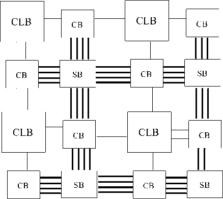
Fig.1. Block diagram of an island style FPGA [5, 6]
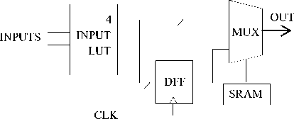
Fig.2. Block diagram of a basic CLB
A k-LUT consist of a set of multiplexers that implement any function of k inputs by forwarding one of the 2k configuration bits to the output of the LUT. The desired configurations are set in SRAM cells [7], and each k-input LUT requires 2k SRAM cells.
-
B. Routing Resources:
The routing resources in an FPGA are divided into connection blocks (CB) and switch blocks (SB). Routing consists of wiring tracks running horizontally and vertically within the FPGA chip. They can be interconnected inside the switch boxes using programmable switches [5, 6]. The purpose of connection blocks is to connect the inputs and outputs of CLB to the routing tracks [5, 6]. The detailed architecture of a 4 CLB FPGA prototype is presented in Fig. 3.
In Fig. 3, the bold lines indicate the routing tracks. For convenience, we have considered 3 horizontal and 2 vertical routing tracks in the Figure. The dotted regions indicate the input connection block and output connection block. Since only one track can connect to any one input, we use multiplexers for connecting the inputs of the CLB to the routing tracks. However, output of a CLB can be connected to any number of tracks and hence pass transistors are used. On the other hand switch blocks are the intersection between the horizontal and vertical routing tracks. The programmable switches are developed by the use of pass gates using only NMOS transistors [8].
-
III. Proposed Approach
In this work, a new FPGA architecture is proposed which includes a control circuitry for power gating unused CLB’s as well as routing resources in the FPGA during runtime. In order to do so, a CLB priority technique is proposed where the concerned CLB’s are analysed on the basis of priority order. We have carried out our approach considering a FPGA prototype consisting of 4 CLB’s. Along with the CLB’s, the gating approach is also extended to the connection blocks associated with each CLB. As depicted in Fig. 3, the input connection blocks (ICB) are combinations of MUX and line buffers. Each input to the CLB is associated with one MUX and corresponding ‘n’ number of Buffers (n = number of MUX inputs). Hence, if we consider a 4 input CLB, 4 MUX and correspondingly 4n Buffers are associated with it. This phenomenon can be observed from Fig. 3, where a 3 input MUX is considered and hence 3 track buffers are associated with its operation. For convenience, we have shown only 1 input of the CLB.
Similarly, if we consider the output connection blocks (OCB) associated with a CLB (Fig. 3), it can be observed that ‘m’ number of Buffers and corresponding pass transistors are associated with each output of the CLB. Here, ‘m’ represents the total number of routing tracks to which the output of a CLB is connected. In our analysis, we have considered 4 input CLBs, however, for the sake of simplicity; we will be depicting only one input and one output of the CLBs in the Figures.
Each CLB in Fig 3 is associated with input as well as output connection blocks. If CLB1 is required to be shut down during inactive periods, the entire dotted regions can also be shut down. However, as we can observe from Fig 3, the buffers associated with the MUXs are also required for the operation of CLB 2. Hence, a CLB priority technique is proposed, so as to decide the criteria to shut down the Buffers during inactive periods. In this work, a CLB priority technique is proposed, where each CLB’s in a set of CLBs are given a priority order, based on which the gating is carried out. The FPGA architecture in this work is divided into clusters of CLB and associated routing architectures. At first, we have considered a cluster of 4 CLBs and extended our proposed approach to 8 CLBs. For the placement [9] of functional modules into the 4 CLBs (CLB1, CLB2, CLB3 and CLB4) in Fig. 3, the following priority order is followed:
CLB1 > CLB2 > CLB3 > CLB4
Thus, when we want to implement functional modules into the CLBs, CLB1 will be used first followed by CLB2 and so on. The power gating state will be decided on the basis of how many CLBs are active at a time. Considering our case in Fig. 3, there can be 5 states:
0 CLB ‘ON’ and 4 CLB ‘OFF’
1 CLB ‘ON’ and 3 CLB ‘OFF’
2 CLB ‘ON’ and 2 CLB ‘OFF’
3 CLB ‘ON’ and 1 CLB ‘OFF’
4 CLB ‘ON’ and 0 CLB ‘OFF’
VDD
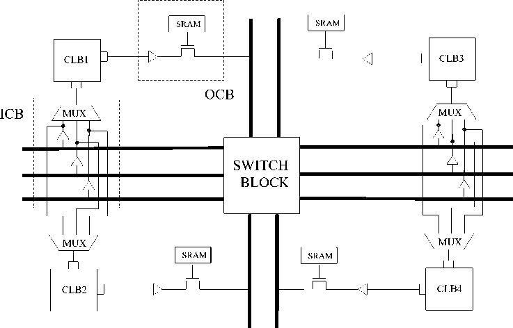
Fig.3. Detailed architecture of a 4 CLB FPGA prototype
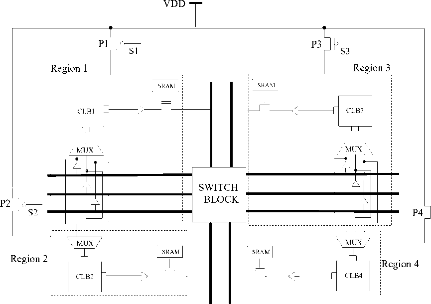
Since, 4 CLBs are present in the cluster, we require 4 sleep transistors to perform power gating individually for the CLBs (and routing resources). The architecture of Fig. 3 is subsequently divided into 4 regions based on the priority order, presented in Fig. 4. The 4 sleep transistors (PMOS) are P1, P2, P3 and P4, with the corresponding sleep signals S1-S4. Based on the switching of the 4 sleep transistors, the 4 regions can be switched ‘off’ or ‘on’.
-
A. Generation of control circuit
To control the operation of the four regions in Fig. 3, three control inputs are required (A, B and C), since there are 5 states of operation of the CLBs. The following Table 1 represents the state table for the generation of sleep signals.
Table 1. State table for the generation of sleep signals
|
Input |
CLB State |
Sleep Signal |
|||||
|
A |
B |
C |
S’1 |
S’2 |
S’3 |
S’4 |
|
|
0 |
0 |
0 |
0 ‘ON’ and 4 ‘OFF’ |
0 |
0 |
0 |
0 |
|
0 |
0 |
1 |
0 ‘ON’ and 4 ‘OFF’ |
0 |
0 |
0 |
0 |
|
0 |
1 |
0 |
0 ‘ON’ and 4 ‘OFF’ |
0 |
0 |
0 |
0 |
|
0 |
1 |
1 |
0 ‘ON’ and 4 ‘OFF’ |
0 |
0 |
0 |
0 |
|
1 |
0 |
0 |
1 ‘ON’ and 3 ‘OFF’ |
1 |
0 |
0 |
0 |
|
1 |
0 |
1 |
2 ‘ON’ and 2 ‘OFF’ |
1 |
1 |
0 |
0 |
|
1 |
1 |
0 |
3 ‘ON’ and 1 ‘OFF’ |
1 |
1 |
1 |
0 |
|
1 |
1 |
1 |
4 ‘ON’ and 0 ‘OFF’ |
1 |
1 |
1 |
1 |
Inputs A, B and C are the control inputs. Based on Table 1, the sleep signals are generated. The formulation of the sleep signals follows the priority order described earlier.
Following constraints are maintained for implementing the gating technique:
-
• When 1 CLB is required to implement a given functional module, CLB1 will be given the preference and consequently S1 is active.
-
• When 2 CLBs are required to be operative, CLB1 and CLB2 will be given the preference and consequently S1 and S2 is active.
-
• When 3 CLBs are required to be operative, CLB1, CLB2 and CLB3 will be given the preference and consequently S1, S2 and S3 are active.
-
• When 4 CLBs are required to be operative, All the CLBs are active and hence all the sleep signals (S1-S4) are active.
-
• When none of the CLBs are required to be operative, all the sleep signals are deactivated, shutting down the power supply to all the four regions in Fig. 4.
Consequently, not only the logic blocks, the routing architectures are also shut down from the power supply. Based on Table 1, the sleep signals required for gating various regions of the FPGA prototype are:
51 = (A)
S4=(ABC)
S 2 = ( AC + AB )
S3=(AB)
The control circuitry based on equations 1-4 is presented in Fig. 5. From Fig. 5, it is observed that inverters are present for the generation of each sleep signal.
S4
Fig.4. Proposed Power gating regions in the 4 CLB FPGA prototype
This is because the sleep transistors are PMOS, and hence we require a logic low input to switch it on. For the ease of the control circuit generation, we have considered the sleep signals in Table 1 to be logic High when the corresponding CLB is required to be active. Hence, we used NOT gates to invert the Logic HIGH outputs of the Control circuit to activate the CLBs. Therefore, in Table 1 the sleep signals are represented as S’1 – S’4, indicating intermediate sleep signals.
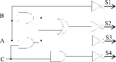
Fig.5. Control Circuit for sleep signal Generation
The final sleep signal supplied to the sleep transistors is the output of the NOT gates presented in Fig. 5.
In our work, we have neglected power gating in Switch blocks. This is because the switch blocks are associated with multiple CLBs and connection blocks at a given time. Generating a control circuit for gating the switch blocks would require a complex circuit and would result in an excess increase of area overhead in the FPGA.
-
B. Importance of Prioritizing the CLBs
The CLBs in the FPGA architecture are first clustered into groups (4 in this case) and each CLB in the cluster are given a priority order. The concept of priority is mainly required to generate the sleep signals to the sleep transistors. Prioritizing the CLBs allows the automated tools to sequentially implement the power gating techniques (in a sequence). If arbitrary implementation of logic in the CLBs were carried out, the activation circuit cannot comply with the changes and different activation circuits had to be designed for each implementation. This is because the sleep signals have to be changed accordingly depending on which CLB is active/inactive, and hence Table 1 has to be modified each time for different implementation. This will not be a feasible process and will significantly increase the area overhead.
-
IV. Extension of Proposed Approach
The proposed approach can also be extended to higher number of CLBs (and associated routing resources). In this section, we analyze the implementation of the proposed approach into 8 CLBs. The FPGA prototype consisting of 8 CLBs and associated routing resources is presented in Fig. 6. Here, we have divided the 8 CLBs (and associated routing resources) into 4 regions and correspondingly we require 4 sleep transistors only (4_SLT_PG method).
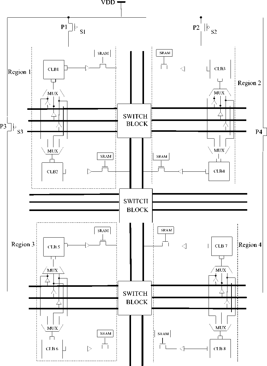
Fig.6. Proposed Power Gating in 8 CLB Prototype
The priority order in this architecture is presented below:
CLB1 > CLB2 > CLB3 > CLB4 > CLB5 > CLB6 > CLB7 > CLB8
The control architecture for generating the sleep signals is similar to the one described in Fig. 5. However, in this case, we will be considering the 4 regions in place of the 4 CLBs.
Hence, based on the 4 regions, 5 states of power gating are possible similar to the 4 CLB architecture. In this architecture, two CLBs are active at the same time i.e. (CLB1 and CLB2), (CLB3 and CLB4), (CLB5 and CLB6) and (CLB7 and CLB8). Corresponding to the two CLBs, the routing resources associated are also activated / deactivated based on the state of the sleep signals (S1 – S4).
Another way of implementing the proposed gating technique to the 8 CLBs is to divide the architectures into 8 regions and hence utilize 8 sleep transistors (8_SLT_PG method). The use of 8 sleep transistors requires the generation of 8 sleep signals and hence the control circuitry will be much larger than the one generated for 4 sleep transistors. On the other hand, the usage of 8 sleep transistors allows us to power gate more CLBs when odd number of CLBs are required to be operative.
For example, when 1 CLB is required to be operative, only CLB1 will be active in case of 8 sleep transistors. However, in case of 4 sleep transistors, both CLB1 as well as CLB2 will be active (Fig. 6). This results in more power savings in 8 sleep transistor approach with respect to 4 sleep transistors. The division of the 8
regions in the 8 sleep transistor approach follows the same principle as in the gating approach in 4 CLBs (Fig. 4). The use of the 8_SLT approach will significantly reduce the leakage power during power gating state, but, comes with a penalty in area.
-
V. Control Inputs and Layout Generation
The control inputs required for gating can be automatically obtained by extracting information from the hardware utilization of the FPGA. After synthesis of the code developed for implementing a functional module into the FPGA, CAD Tools like Xilinx ISE provide the details of the Hardware utilization in the FPGA [10], before implementation of the function into the device. Based on the information of the number of CLB (n) required to implement a given function, the control inputs (A, B, C) can be generated. The algorithm for generation of the control inputs is based on the priority order explained earlier.
The pseudo code for the generation of control inputs (A, B, C) of Fig. 4 is presented below:
Input: n = number of required CLBs Output : A, B, C
Start if (n == 0) //0 CLB ‘ON’ and 4 CLB
‘OFF’ then A = 0, B = 0, C = 0;
elseif (n == 1) //1 CLB ‘ON’ and 3
// CLB ‘OFF’ then A = 1, B = 0, C = 0;
elseif (n == 2) //2 CLB ‘ON’ and 2
// CLB ‘OFF’ then A = 1, B = 0, C = 1;
elseif (n == 3) //3 CLB ‘ON’ and 1
// CLB ‘OFF’ then A = 1, B = 1, C = 0;
elseif (n == 4) //4 CLB ‘ON’ and 0
// CLB ‘OFF’ then A = 1, B = 1, C = 1;
end
In order to place the desired functional module within the specific sites in the FPGA, a region-constraint placement technique needs to be adopted. FPGA placement software’s like PlanAhead™ allows the user to assign constraints during placement which may include location constraints to lock specific logic objects into specific sites on the device or area constraints to constrain a group of logic within a specific area of the device [9].
The layout of the proposed power gated FPGA prototype has been developed in CADENCE LAYOUT TOOL and resulted in correct DRC (Design Review Check) and LVS (Layout vs. Schematic) analysis. The Fig. 7 represents the layout schematic of proposed power gated ‘4 CLB FPGA’ prototype.
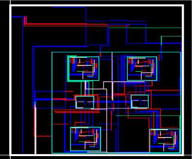
Fig.7. Layout of the proposed power gated ‘4 CLB FPGA’
Timing is a critical factor in power gated designs. The delay in a power gated FPGA mainly increase due to the wake up time associated with the power gated blocks. Wake up time associated with power gating accounts for the turn-on time required by the sleep transistor to transit from an inactive mode to active mode. This delay is required to limit the sudden ‘surge current’ during the waking up process [12]. An efficient way of reducing the wake-up time associated with power gating is to increase the width of the sleep transistor. However, with increase in sleep transistor width, the power savings reduces as power dissipation is directly proportional to the width of a transistor.
-
VI. Experimental Results
The design and simulations of the FPGA prototypes in this work have been carried out in CADENCE virtuoso spectrum using 45 nm technology. The sleep transistors used in power gating are High threshold voltage PMOS (High VTH). All simulations have been carried out at power supply VDD = 1V. The simulation results have been obtained for both without power gating (WPG) and with power gating (PG) in the FPGA prototypes. The effect of input/output ports has been neglected in this work for avoiding complexity.
-
A . Power Results
The power results obtained for the 4 CLB FPGA prototype (Fig. 4) is presented in the following Table. 3. The power is calculated for all the 5 states of the power gating criteria and compared with ‘without power gated’ prototype. From Table 3, it can be observed that a considerable amount of power savings have been achieved by our proposed approach.
Table 2. Total Power Results of 4 CLB FPGA prototype
|
State of CLB |
Power (uW) |
% savings in PG over WPG |
|
|
WPG |
PG |
||
|
0 ‘ON’ 4 ‘OFF’ |
0.309 |
0.219 |
29.12 |
|
1 ‘ON’ 3 ‘OFF’ |
6.44 |
2.948 |
54.22 |
|
2 ‘ON’ 2 ‘OFF’ |
6.44 |
3.54 |
45.03 |
|
3 ‘ON’ 1 ‘OFF’ |
12.81 |
8.47 |
33.87 |
|
4 ‘ON’ 0 ‘OFF’ |
12.81 |
11.29 |
11.86 |
A maximum of 54.22% power saving is achieved during the 1 ‘ON’ 3 ‘OFF’ state, after power gating (PG). From the concept of the power gating technique the 0 ‘ON’ 4 ‘OFF’ state should produce the maximum saving, however, since none of the CLBs are functioning in this state, only leakage power is dissipated here. And hence the power dissipation is less compared to other states and as a result power savings is also less.
-
B. Area Results
Area reports are generated in terms of the total transistor count of the architecture and multiplying with ‘k’, which is the width of a minimum width transistor [11]. The total area is represented in terms of ‘λ2’ where ‘λ’ stands for the feature size of a particular technology. The area reports of our proposed approach are presented in Table 4. The proposed power gating technique results in a minimal penalty of area overhead. The area overhead percentage further reduces with the increase in number of CLBs. This can be observed from Fig 8, where the variation of area overhead percentage for 4_SLT_PG of various CLB clusters is analyzed. As the number of CLB keeps on increasing, the area overhead reduces. Increasing the number of sleep transistor with the increase in number of CLB will not be a feasible process as it will require more hardware off-chip for designing the control circuit. A better method would be to cluster the CLBs into groups and each group can be controlled by a single sleep transistor. Hence, in our approach, we have only analyzed the area overhead considering 4 sleep transistors and 8 sleep transistors for higher number of CLBs.
Table 3. Area analysis of proposed approach
|
No. of CLB |
No. of Gating regions |
No. of sleep transistor |
Total Area (λ2) |
Area overhe ad (%) in PG over WPG |
|
|
WPG |
PG |
||||
|
4 |
4 |
4 |
1936k |
1972k |
1.859 |
|
8 |
4 |
4 |
3968k |
4004k |
0.907 |
|
8 |
8 |
8 |
3968k |
4038k |
1.764 |
|
16 |
4 |
4 |
7840k |
7876k |
0.459 |
|
16 |
8 |
8 |
7840k |
7910k |
0.892 |
|
32 |
4 |
4 |
15584k |
15620k |
0.231 |
|
32 |
8 |
8 |
15584k |
15654k |
0.449 |
|
64 |
4 |
4 |
31072k |
31108k |
0.115 |
|
64 |
8 |
8 |
31072k |
31142k |
0.225 |
|
128 |
4 |
4 |
62048k |
62084k |
0.058 |
|
128 |
8 |
8 |
62048k |
62118k |
0.112 |
|
128 |
16 |
16 |
62048k |
62189k |
0.227 |
In case of 128 CLBs, we have analyzed the impact of 16_SLT_PG also, where 16 sleep transistors were considered. The area overhead for a 128 CLB FPGA is a mere 0.058% for the 4_SLT_PG approach, 0.112% for 8_SLT_PG approach and 0.227% for 16_SLT_PG approach.
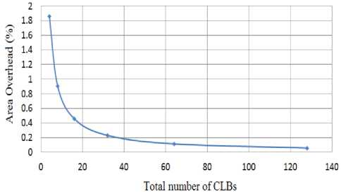
Fig.8. Variation of Area overhead with total no. of CLBs (4 SLT_method)
The activation circuit will be similar for all higher CLB FPGAs implementing the 4_SLT_PG and 8_SLT_PG. In case of 16_SLT_PG approach, 5 control inputs are required to implement the activation function. However, to gain more power savings higher number of sleep transistors will be preferred.
-
C . Delay Analysis
The delay results associated with the power gated ‘4 CLB FPGA’ is presented in this section. The delay is measured in terms of wake up time of the power gated blocks. The wake-up phenomenon in power gated blocks is explained in the Following Fig. 9,
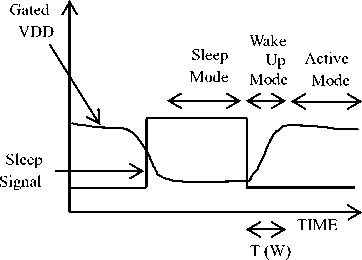
Fig.9. Wake up time ‘T (W)’ associated with power gated blocks
Depending upon the sleep signal, the time required by the gated supply voltage (Gated VDD) to reach its maximum value is termed as the wake-up time. The analysis of the wake-up time measured in our approach is presented in Table 4.
Table 4. Wake up time analysis of proposed approach
|
Sleep Transistor Width (nm) |
Wake Up time (ns) |
|
120 |
3.45 |
|
180 |
2.99 |
|
240 |
2.33 |
|
300 |
2.12 |
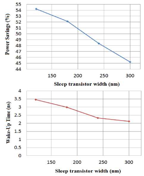
Fig.10. Variation of power savings and Wake up time with respect to sleep transistor width.
In Table 4, the wake up time is analysed for 4 different width of the sleep transistor (120 nm, 180 nm, 240 nm and 300 nm). It is evident from Table 4 that wake-up time reduces with the increase in width of sleep transistor (Fig. 10) and as a result delay reduces. However, with this reduction of delay, the total power savings after gating also gets affected (Fig. 10). The power savings will reduce with the increase in width of sleep transistor, as power dissipation is directly proportional to width of the transistor [11].
-
VII. Conclusion
In this work, an efficient technique of autonomous power gating is proposed in FPGA architecture, based on a CLB priority technique. The power gating is introduced to selectively shut down the power supply to the unused blocks of the FPGA during runtime. The FPGA architecture is divided into clusters of CLBs and associated routing resources and gating is introduced separately in each cluster. A CLB priority placement technique is proposed for implementing power gating. Simulations have been carried out for 4 CLB and 8 CLB FPGA prototype. The schematic and Layout of the prototype have been designed in CADENCE Analog design tool at 45 nm technology. Simulation results show that up to 55% power reduction is achieved in a ‘4 CLB’ FPGA prototype after implementation of the proposed gating technique. The idea of extending the proposed approach to 8 CLB prototypes is also presented in this paper. The area overhead in the proposed approach tends to reduce as the number of CLBs is increased.
In a 128 CLB FPGA prototype, the area overhead stands at a mere 0.058 %, considering 4 sleep transistors. The wake up time associated with the power gated blocks reduces with the increase in sleep transistor width.
Acknowledgement
This work is supported by SMDP-C2SD project, sponsored by Deity, Govt. of India.
References A CLB priority based power gating technique in field programmable gate arrays
- H. Z. V. George and J. Rabaey, “The design of a low energy FPGA,” in Proc. Int. Symp. Low Power Electron.Des., CA, Aug. 1999, pp.188–193.
- S. Ishihara, M.Hariyama, and M. Kameyama, “A Low-Power FPGA Based on Autonomous Fine-Grain Power Gating”, IEEE Transactions on Very Large Scale Integration (VLSI) Systems, Vol. 19, No. 8, August 2011.
- Jason H. Anderson,Farid N. Najm, “Low-Power Programmable FPGA Routing Circuitry”, IEEE Transactions on Very Large Scale Integration (VLSI) Systems, Vol. 17 , No. 18, pp. 1048-1060, 2009.
- Assem A. M. Bsoul, Steven J. E. Wilton, “An FPGA architecture supporting dynamically controlled power gating”, International Conference on Field-Programmable Technology, pp. 1-8, Dec. 2010.
- Paul Chow, Soon Ong Seo, Jonathan Rose, Kevin Chung, Gerard P´aez-Monz´on, and Immanuel Rahardja, “The Design of an SRAM-Based Field-Programmable Gate Array—Part I: Architecture”, IEEE Transactions on Very Large Scale Integration (VLSI) Systems, Vol. 7, No. 2, June 1999.
- Paul Chow, Soon Ong Seo, Jonathan Rose, Kevin Chung, Gerard P´aez-Monz´on, and Immanuel Rahardja, “The Design of an SRAM-Based Field-Programmable Gate Array—Part II: Circuit Design and Layout”, IEEE Transactions on Very Large Scale Integration (VLSI) Systems, Vol. 7, No. 3, June 1999.
- Gupta, V., & Anis, M., “Statistical Design of the 6T SRAM Bit Cell”, IEEE Transactions on Circuits and Systems I, Vol. 57, No. 1, pp. 93-104, 2009.
- H. Schmit, V. Chandra, “Layout techniques for FPGA switch blocks”, IEEE Transactions on Very Large Scale Integration (VLSI) Systems, Vol. 13, No. 1, Jan. 2005
- www.xilinx.com/support/documentation/sw_ manuals/xilinx11/ise_c_constraints_planahead.htm
- www.xilinx.com/support/documentation/sw_ manuals/xilinx11/sim.pdf
- Nag, D. Nath, and S. N. Pradhan, “Leakage Reduction of SRAM-Based Look-Up Table Using Dynamic Power Gating”, Journal of Circuits, Systems and Computers, Vol. 26, No. 03, March 2017.
- Vivek, T.D., Sentieys, O., Derrien, S., “Wakeup Time and Wakeup Energy Estimation in Power-Gated Logic Clusters”, 24th International Conference on VLSI Design (VLSI Design), 2011, pp. 340-345.
- H. A. Elreesh, B. Hamed, “FPGA Fuzzy Controller Design for Magnetic Ball Levitation”, I.J. Intelligent Systems and Applications, 2012, Vol. 10, pp. 72-81.
- Sanjay Singh, Sumeet Saurav, Chandra Shekhar, Anil Vohra,"Prototyping an Automated Video Surveillance System Using FPGAs", International Journal of Image, Graphics and Signal Processing(IJIGSP), Vol.8, No.8, pp.37-46, 2016.
- Sanjay Singh, Anil K Saini, Ravi Saini,"Interfacing the Analog Camera with FPGA Board for Real-time Video Acquisition", IJIGSP, vol.6, no.4, pp.32-38, 2014.DOI: 10.5815/ijigsp.2014.04.04
- Shoaib Shokuhi, Ali Hosseini,"Power Optimization of Configurable Logic Block in FPGA via Controlling Logic State of Virtual Ground Voltage", International Journal of Image, Graphics and Signal Processing(IJIGSP), Vol.8, No.2, pp.45-52, 2016.
