A compact design of a balanced 1x4 optical power splitter based on silicon on insulator slot waveguides

Author: Butt Muhammad Ali, Naresh Kumar Reddy Andra, Khonina Svetlana Nikolaevna
Journal: Компьютерная оптика @computer-optics
Section: Дифракционная оптика, оптические технологии
Article in issue: 2 т.42, 2018.
Free access
In this paper, a compact design of a balanced 1×4 optical power splitter based on coupled mode theory (CMT) is presented. The design consists of seven vertically slotted waveguides based on the silicon-on-insulator platform. The 1×4 OPS is modelled using commercial finite element method (FEM) simulation tool COMSOL Multiphysics 5.1. The optimized OPS is capable of working across the whole C-band with maximum ~39 % of power decay in the wavelength range 1530 - 1565 nm.
Slot waveguides, 1×4 power splitter, soi, c-band, finite element method
Short address: https://sciup.org/140228722
IDR: 140228722 | DOI: 10.18287/2412-6179-2018-42-2-244-247
Text of the scientific article A compact design of a balanced 1x4 optical power splitter based on silicon on insulator slot waveguides
Research on silicon photonics can be dated back to the 1980s. Though, the previous decade has observed an extraordinary development in the field. Based on highly advance silicon semiconductor technology, silicon photonics would deliver with an inexpensive, highly integrated electronic-photonic platform, in which ultracompact photonic devices and electronic circuits are converged. The fundamental motive behind silicon photonics is the ability to use CMOS-like fabrication resulting in high-volume production at low cost [1]. Optical power splitters (OPS) play a fundamental role in optical communication systems [2, 3] and periodic optical sources for integrated microfluidic devices [4]. These optical elements are substantial for conveying the optical fiber to end-users [5]. OPSs are principally based on either Y-branch splitters [3, 6, 7] or multimode interference (MMI) splitters [8–10]. Generally, the former is more compact but the optimization of their branch region is complicated. The latter is simpler, while it has large modal interaction length. For optical elements based on modal interference, reduction of the modal interaction length can result in increased sensitivity to fabrication tolerances and therefore can sacrifice device robustness. For instance, shortening the interaction length of directional couplers by reducing the gap between waveguides can affect the fabrication tolerances, which are already very low due to the comparatively tight guiding that is characteristic of semiconductor waveguides.
There are several designs of OPS, which are proposed recently. 1×2 and 1×3 Ultra compact power splitters based on the horizontal nano-plasmonic slot waveguides are proposed [11]. A 1×4 OPS based on multimode interference (MMI) coupler in silicon (Si)-gallium nitride (GaN) slot waveguide structure is presented. This device can be useful to divide optical signal energy uniformly in the C-band range into four output ports [12]. In [13] 1×4 OPS is proposed by combining three 1×2 OPS based on two-mode interference (TMI) effects in slot waveguides.
An exceptional waveguide geometry known as a slot waveguide is presented by Almeida et al in 2004 where the guided light is strongly confined within a narrow low-index slot (S) between the two high indices photonic wires [14, 15]. There are two claddings (high index material) separated from each other with a narrow slot (low index material) [16, 17]. The electric field propagating in the slot suffers a disruption at the high refractive index contrast interface which makes the electromagnetic wave to confine intensely in the narrow slot than in the cladding which can lead to the implementation of compact and high-performance photonic components such as resonators [18] and polarization beam splitters [19, 20]. Moreover, there are no confinement losses in the slot waveguide structure due to the strong high power confinement inside the slot area. Therefore, there is a noteworthy attention in designing photonic devices based on a slot waveguide structure that integrates semiconductor materials.
In this paper, we modelled 1×4 OPS of size 8 µm based on coupled-mode theory (CMT) [21] by using seven vertically slotted waveguides at 1550 nm TE-po-larized light. Numerical optimizations were performed on the coupling gap (C1, C2 and C3) between the slot waveguides structures (by keeping the coupling lengths constant) in order to obtain an equal power distribution among 4 outputs. The CMT is used to evaluate the mode coupling or conversion in optical waveguides. The physical models for coupled waveguide systems contain two or more dielectric waveguides employed in close proximity. These waveguides maybe parallel to each other or may have variable separations. The slot waveguide core is composed of two Si ( n = 3.48) slab surrounding a narrow slot. The slot is simply an air ( n = 1). The splitter schematic structure is shown in fig. 1. And the slot waveguide cross section is depicted by the inset. All the simulations are performed by using Comsol Multiphysics 5.1 which solves the Helmholtz equation with the finite element method (FEM).
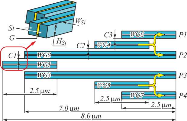
Fig. 1. Schematic of a 1×4 OPS
1×4 OPS model
In our proposed design, we used seven vertically slotted waveguides in order to form a compact 1×4 OPS. WSi, HSi and G are chosen at 150 nm, 220 nm and 40 nm respectively, in order to acquire a maximum confinement in the slot region and ensure a fundamental TE mode in the proposed power splitter. The WGs are placed in a close proximity so that the evanescent modes of one WG overlap with the modes of a second guide. The light from one WG gradually transfers back and forth between the WGs. It is possible to couple any desired faction of light from one WG to other by choosing the separation between the WGs and length of the coupling region,
The length of WG1, WG4, WG5, WG6 and WG7 is fixed at 2.5 µm which provides an adequate coupling length between the adjacent WGs. While the length of the WG2 and WG3 is 7 µm which serves as output at port 2 and port 3. The output from WG6 and WG7 is collected at port 1 and port 4. Hereafter, we will only focus on the coupling gap in order to obtain the balanced OPS.
Likewise, C 1, C 2 and C 3 are the coupling gap between WG1-WG2/WG3, WG2/WG3-WG4/WG5, WG4/WG5-WG6/WG7, respectively. In COMSOL simulations, the subdomains in the WG cross section were divided into triangular mesh elements. The grid size is set to λ /15 for the WGs geometries and λ /8 for the air domain so that precise simulation results can be obtained within the available computational resources. Scattering boundary conditions were applied at the outer edges of the FEM simulation window to estimate an open geometry.
Optimization of coupling gap, C1
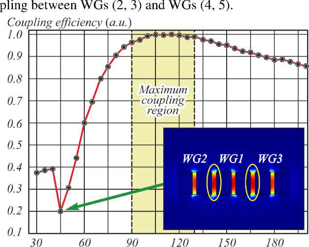
The coupling strength can be very sensitive to the distance between the WGs and it is significant to ultimately pick a design that can function adequately given the type of deficiencies that are expected from the manufacturing process. In the first stage, C 1 is varied from 30–200 nm between WG1 and the adjacent WGs (2 and 3). The coupling efficiency of C 1 is plotted in fig. 2. It can be seen that when C 1 <45 nm, the energy doesn’t transfer to the adjacent WGs instead it confines itself in C 1. This happens because the gap is too small that it behaves as another slot WG and tries to confine the energy in C 1. Therefore, an optimal separation between two WGs is important in order to obtain the maximum coupling.
A maximum coupling efficiency is obtained at values between 90– 125 nm where the power is equally divided between WG2 and WG3 with less coupling losses. Hence, we used an optimal value of C 1 = 115 nm in our splitter design for maximum coupling. Based on these results, C 2 is also fixed at 115 nm to obtain maximum cou-
Coupling gap, Cl (nm)
Fig. 2. Coupling efficiency C1 versus coupling gap
Optimization of coupling gap, C3
In order to obtain the balanced 1×4 OPS, C 3 has to be slightly adjusted. If we consider on the right half of the power splitter, we can see that the energy from WG5 is transferred to WG7 and some part of the energy is coupled back to WG3. The distribution of the power between WG3 and WG7 is not equal as seen in fig. 3 where normalized intensity distribution at port 1, port 2, port 3 and port 4 are shown for various values of C 3.
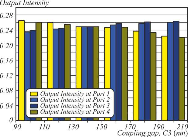
Fig. 3. Coupling gap, C3 versus intensity distribution at port 1, port 2, port 3 and port 4
For values of C 3 < 140 nm, the output intensity at Port 2 and Port 3 is less than Port 1 and Port 4. For instance: at C 3 = 120 nm, the intensity obtained at port 1, port 2, port 3 and port 4 is 26%, 24.2%, 24.4% and 25.4% respectively. Whereas on the other hand, when C 3 increases, the intensity in Port 2 and Port 3 also increases gradually.
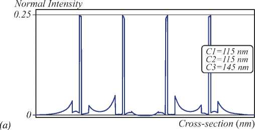
The optimized value of C3 is obtained at 140 nm where the OPS is balanced with 25 % of power transmission at each port as shown in fig. 3. The line graph and the nor- malized intensity contour plots at Port 1, Port 2, Port 3 and Port 4 are shown in fig. 4a and fig. 4b, respectively.
02+03 , _CL i .Cl.. 02+03
----------w г»---»4»---»-| и»----------
Output Output i Output Output port 1 port 2 port 3 port 4
(b)
Fig. 4. Normalized intensity at Port 1, Port2, Port3 and Port 4, (a) Line graph, (b) Contour plot
Performance of an optimized balanced 1×4 OPS over whole C-band (1530 – 1565 nm)
In IR optical communications, C-band refers to the wavelength range 1530-1565 nm, which corresponds to the amplification range of erbium-doped fiber amplifier (EDFA). The 1×4 OPS was designed and optimized at 1550 nm. The performance of the power splitter was analysed and found that there is a maximum ~ 39 % of power decay across the whole C-band as can be seen in fig 5. The parametric sweep function is used to calculate the electric field in the slot with a wavelength increment of 2. The designed power splitter remains balanced over the wavelength range of 1530–1565 nm.
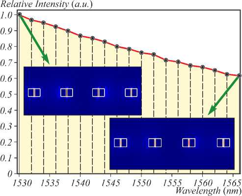
Fig. 5. Relative intensity at the output of the 1×4 OPS versus wavelength
Conclusion
In this paper, we presented a compact 1×4 balanced OPS based on silicon on insulator by using seven slot waveguides at TE polarization. This power splitter is capable of operating in whole infrared optical communication C-band (1530–1565 nm). Our designed splitter is a promising candidate for high-density photonic integrated circuit due to its ultra-short length and excellent performance. Based on this design, splitters with various power distributions at the output can be established by varying the coupling gap. In future, we would like to extend this study to demonstrate similar OPS with a large number of output ports.
References A compact design of a balanced 1x4 optical power splitter based on silicon on insulator slot waveguides
- Bogaerts, W. Nanophotonic waveguides in Silicon-on-Insulator fabricated with CMOS technology/W. Bogaerts, R. Baets, P. Dumon, V. Wiaux, S. Beckx, D. Taillaert, B. Luyssaert, J. Van Campenhout, P. Bienstman, D. Van Thourhout//Journal of Lightwave Technology. -2005. -Vol. 23, Issue 1. -P. 401-412. - DOI: 10.1109/JLT.2004.834471
- Huang, J.Z. A new design approach to large input/output number multimode interference couplers and its application to low-cross talk WDM routers/J.Z. Huang, R. Scarmozzino, R.M. Osgood//IEEE Photonics Technology Letters. -1998. -Vol. 10, Issue 9. -P. 1292-1294. - DOI: 10.1109/68.705620
- Butt, M.A. Fabrication of Y-splitters and Mach-Zehnder structures on (Yb, Nb):RTiOPO4/RbTiOPO4 epitaxial layers by reactive ion etching/M.A. Butt, R. Solé, M.C. Pujol, A. Ródenas, G. Lifante, A. Choudhary, G.S. Murugan, D.P. Shepherd, J.S. Wilkinson, M. Aguiló, F. Díaz//Journal of Lightwave Technology. -2015. -Vol. 33, Issue 9. -P. 1863-1871. - DOI: 10.1109/JLT.2014.2379091
- Mogensen, K.B. A microfluidic device with an integrated waveguide beam splitter for velocity measurements of flowing particles by Fourier transformation/K.B. Mogensen, Y.C. Kwok, J.C.T. Eijkel, N.J. Peterson, A. Manz, J.P. Kutter//Analytical Chemistry. -2003. -Vol. 75, Issue 18. -P. 4931-4936. - DOI: 10.1021/ac034427a
- Phillips, A.J. Redundancy strategies for a high splitting optically amplified passive optical network/A.J. Phillips, J.M. Senior, R. Mercinelli, M. Valvo, P.J. Vetter, C.M. Martin, M.O. van Deventer, P. Vaes, X.Z. Qiu//Journal of Lightwave Technology. -2011. -Vol. 19, Issue 2. -P. 137-149. - DOI: 10.1109/50.917866
- Gamet, J. Field matching Y-branch for low power splitter/J. Gamet, G. Pandraud//Optics Communications. -2005. -Vol. 248, Issues 4-6. -P. 423-429. - DOI: 10.1016/j.optcom.2004.12.040
- Butt, M.A. Channel waveguides and Mach-Zehnder structures on RbTiOPO4 by Cs+ ion exchange/M.A. Butt, M.C. Pujol, R. Sole, A. Rodenas, G. Lifante, J.S. Wilkinson, M. Aguilo, F. Diaz//Optical Materials Express. -2015. -Vol. 5, Issue 5. -P. 1183-1194. - DOI: 10.1364/OME.5.001183
- Kim, J.H. Experimental demonstration of replicated multimode interferometer power splitter in Zr-doped sol-gel/J.H. Kim, B.W. Dudley, P.J. Moyer//Journal of Lightwave Technology. -2006. -Vol. 24, Issue 1. -P. 612-616. - DOI: 10.1109/JLT.2005.859849
- Chen, B. Flexible optical waveguide beam splitters based on directional coupling/B. Chen, L. Huang, Y.D. Li, C.L. Liu, G.Z. Liu//Journal of the Optical Society of America B. -2011. -Vol. 28, Issue 11. -P. 2680-2684. - DOI: 10.1364/JOSAB.28.002680
- Yu. T.B. Ultracompact 2x2 photonic crystal waveguide power splitter based on self imaging effect realized by asymmetric interference/T.B. Yu, Q.J. Wang, J. Zhang, J.Y. Yang, S.F. Yu//IEEE Photonics Technology Letters. -2011. -Vol. 23, Issue 16. -P. 1151-1153. - DOI: 10.1109/LPT.2011.2154360
- Zhu, S. Nanoplasmonic power splitters based on the horizontal nanoplasmonic slot waveguide/S. Zhu, G.Q. Lo, D.L. Kwong//Applied Physics Letters. -2011. -Vol. 99, Issue 3. -031112. - DOI: 10.1063/1.3615306
- Malka, D. A photonic 1x4 power splitter based on Multimode Interference in Silicon-Gallium-Nitride slot waveguide structures/D. Malka, Y. Danan, Y. Ramon, Z. Zalevsky//Materials. -2016. -Vol. 9, Issue 7. -P. 516-523. - DOI: 10.3390/ma9070516
- Chen, B. Design of broadband power splitters using two-mode interference in slot waveguides/B. Chen, C. Liu, J. Si//Optics Communication. -2015. -Vol. 355. -P. 367-375. - DOI: 10.1016/j.optcom.2015.07.009
- Almeida, V.R. Guiding and confining light in the void nanostructure/V.R. Almeida, Q. Xu, C.A. Barrios, M. Lipson//Optics Letters. -2004. -Vol. 29, Issue 14. -P. 1209-1211. - DOI: 10.1364/OL.29.001209
- Xu, Q.F. Experimental demonstration of guiding and confining in nanometer-size low-refractive-index material/Q.F. Xu, V.R. Almeida, R.R. Panepucci, M. Lipson//Optics Letters. -2004. -Vol. 29, Issue 14. -P. 1626-1628. - DOI: 10.1364/OL.29.001626
- Butt, M.A. Silicon on silicon dioxide slot waveguide evanescent field gas absorption sensor/M.A. Butt, S.N. Khonina, N.L. Kazanskiy//Journal of Modern Optics. -2018. -Vol. 65, Issue 2. -P. 174-178. - DOI: 10.1080/09500340.2017.1382596
- Degtyarev, S.A. Modeling of TiO2 based slot waveguides with optical confinement in sharp bends/S.A. Degtyarev, M.A. Butt, S.N. Khonina, R.V. Skidanov//Proceedings of the 2016 International Conference on Computing, Electronic and Electrical Engineering (ICE Cube). -2016. -7495222. - DOI: 10.1109/ICECUBE.2016.7495222
- Barrios, C.A. Demonstration of slot-waveguide structures on silicon nitride/silicon oxide platform/C.A. Barrios, B. Sánchez, K.B. Gylfason, A. Griol, H. Sohlström, M. Holgado, R. Casquel//Optics Express. -2007. -Vol. 15, Issue 11. -P. 6846-6856. - DOI: 10.1364/OE.15.006846
- Fujisawa, T. Polarization-independent optical directional coupler based on slot waveguides/T. Fujisawa, M. Koshiba//Optics Letters. -2006. -Vol. 31, Issue 1. -P. 56-58. - DOI: 10.1364/OL.31.000056
- Dai, D. Ultra short broadband polarization beam splitter based on an asymmetrical directional coupler/D. Dai, Z. Wang, J.E. Bowers//Optics Letters. -2011. -Vol. 36, Issue 13. -P. 2590-2592. - DOI: 10.1364/OL.36.002590
- Huang, W.P. Coupled-mode theory for optical waveguides: an overview/W.P. Huang//Journal of the Optical Society of America A 1994; 11(3): 963-983 DOI: 10.1364/JOSAA.11.000963
