A High-Performance Communication Service for Parallel Servo Computing

Author: Cheng Xin, Zhou Yunfei, Hu Yongbin, Kong Xiangbin
Journal: International Journal of Modern Education and Computer Science (IJMECS) @ijmecs
Article in issue: 1 vol.2, 2010.
Free access
Complexity of algorithms for the servo control in the multi-dimensional, ultra-precise stage application has made multi-processor parallel computing technology needed. Considering the specific communication requirements in the parallel servo computing, we propose a communication service scheme based on VME bus, which provides high-performance data transmission and precise synchronization trigger support for the processors involved. Communications service is implemented on both standard VME bus and user-defined Internal Bus (IB), and can be redefined online. This paper introduces parallel servo computing architecture and communication service, describes structure and implementation details of each module in the service, and finally provides data transmission model and analysis. Experimental results show that communication services can provide high-speed data transmission with sub-nanosecond-level error of transmission latency, and synchronous trigger with nanosecond-level synchronization error. Moreover, the performance of communication service is not affected by the increasing number of processors.
Communication service, Parallel computing, VME bus, data transmission
Short address: https://sciup.org/15010045
IDR: 15010045
Text of the scientific article A High-Performance Communication Service for Parallel Servo Computing
Published Online November 2010 in MECS
In the 65nm twins-wafer-stages Lithography, three 6-DOF (Degrees Of Freedom) stages exist and more than 40 axles need to be controlled. The complexity of algorithms has led to the performance requirement exceeding the capabilities of a single processor; therefore, multi-processor parallel computing technology is needed [1] [2]. The parallel servo computing discussed in the paper has the following requirements on communication service: (1) in every parallel computing cycle, a large number of data need to be transmitted among various processors. The transmission latency must be low and accurate otherwise its uncertainty will disorder the timing sequence of parallel servo calculation; (2) Due to the complex coupling relations in the movements of related axes, the inconsistent output delay of control command will damage control model [2][3][12]. Hence, precise synchronous trigger is required.
MPI (Message passing interface) is a library specification for message-passing, used widely on certain classes of parallel machines, especially those with distributed memory [4]. The study of MPI and its improvement is relatively richer. However, the communication service based on MPI suffers from the following problem: as the number of processors increases, the data transmission latency will increase significantly [5-8]; more importantly, only the estimate instead of the accurate value of the transmission time of a certain data packet is available and precise synchronous trigger can not be provided, which means that MPI is not suitable for communications service for ultra-high precision parallel servo computing.
Yan Luxin and Zhang Tianxu [10] investigated a "Δ" type shared memory architecture based on FPGA, which achieved accurate transmission latency and relatively high bandwidth among three DSPs. However, the architecture of this shared memory is extremely complex when the complexity of transmission requirements increases (if more DSPs exist in the parallel architecture).
James Kohout and Alan D. George [11] investigated a ring-type data transmission architecture, in which it achieved the bandwidth of 320Mbits/S between neighboring nodes. A problem of this transmission architecture is that ring size expands with the increasing number of nodes; even if pipeline operation is adopted to optimize data transmission, the transmission time of a certain data packet will still increase with ring size expanding.
It is also difficult to achieve precise transmission latency when using TCP or MPI based on Ethernet link [13] [14], because the uncertainty caused by the upper layer protocols (such as data congestion, handshaking and error handling mechanism) makes it difficult to establish precise data transmission model. Even if the high communication bandwidth is achieved, synchronization performance can only achieve 200ns-level [12] or lower, which will generate intolerant synchronization position error that may destroy control model when stage is at high speed.
FPDP (Front Panel Data Port) is probably a good choice. More details on FPDP are introduced in [16]. The main drawback with this method is that when redefinition is needed, all the nodes in the system need reconfiguration. Since no signals are available for addressing on FPDP, the definition of data transmission sequence is done before the data transmission starts [16].
Considering the specific need of communication service, it would be a better choice to adopt hardware architecture to implement data sending, transmission, and storage. Once the transmission timing is set, it would be executed consistently; also both transmission latency and bandwidth depend only on hardware performances. Such properties make the data transmission model more accurate with no extra software overhead. In this paper, we propose a high-performance communication service scheme, which provides high-performance data transmission and precise synchronization trigger support for multi-DSP parallel computing architecture. We design IB (Internal Bus) to construct data transmission channel with high bandwidth and stable transmission performance by using broadcast transmission. Communication service is implemented by FPGA (Field Programmable Gate Array).
-
II. Parallel Servo Computing Architecture and Communication Service
Parallel computing architecture is designed based on VME bus, where the upper computer is the only VME host. On the VME bus, P1connector is defined in the VME64x specification, while several pins in P2 connector are reserved for users’ definition [15] [17]. IB has been defined in these reserved pins. Upper computer can access each processor via standard VME bus (P1) and IB (P2) has been designed as the high-speed data channel among the processors. IBMC (Internal Bus Master Controller) generates bus control signals following the defined IB timing specification. Under the control of those signals, IBSC (Internal Bus Slave Controller) finishes data transmission and generates synchronous trigger following the defined synchronous timing specification to synchronize parallel computing of multiDSP. VME_Ctrller provides interface to standard VME64x bus for IBMC, IBSC and DSP. To realize control and management towards IB, upper computer configures IBMC via VME interface to define the “behavior” of IB. The data transmission process on IB does not involve the participation of DSP software.
The object discussed in this paper is the communication service composed of VME bus, VME_Ctrller, IB, IBMC, and IBSC, as shown in dashed frame in Fig.1. Communication service includes data transmission and synchronous trigger functions.
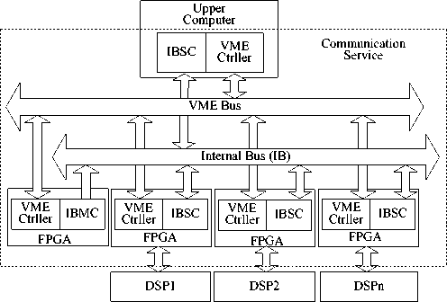
Fig.1. Parallel servo computing architecture
Data transmission is implemented on both VME bus and IB. Data sent by upper computer via VME bus contain task parameters to DSPs and configuration to IBMC (or IBSC). Other than sending all the data simultaneously, the upper computer sends data successively according to the slave address of each VME in the address map. Due to handshaking and arbitration involved in data transmission process on VME bus, it is
Sending Task Parameters
Configuring
1BMC A
VME Bus
Idle
Configuring 1BSC
The First Parallel Computing Cycle
Idle
Time Difference

Recerving Tasks Parameters
Data Transmission sequence
Data Insensitive

Computing

Trigger 2
Trigger 1
Data Sensitive
The Nst Parallel
Data
Computing Cycle
Insensitive
Computing Computing
Data Sensitive Computing
Trigger 1
Trigger 2
Trigger 1
Synchronous Trigger
Relaxed timing transmission

Time
Strict timing
1 transmission
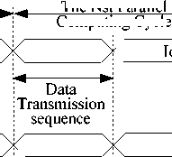
Fig.2. Functions of communication service relatively difficult to calculate precise transmission latency; moreover, the time difference between data receiving of different VME slave exists in the data transmission on VME bus. For these reasons, the data transmission on VME is defined as relaxed timing transmission. In contrast, the design for IB transmission is simple and strict, which happens in every parallel cycle to implement data exchange among DSPs.
The functions of communication service are described in Fig.2. Synchronous trigger ensures simultaneous startup of calculation and simultaneous output of result in every parallel computing cycle. Trigger 1 is generated at the moment data transmission sequence begins on IB to inform DSP that only data-insensitive calculations can be implemented. Furthermore, the result of previous cycle will be outputted synchronously under the action of trigger 1. Trigger 2 is generated at the moment data transmission ends to start data-sensitive calculation, and IB remains idle until the end of current parallel computing cycle. The difference between data-sensitive and data-insensitive calculation is that for the former, the access IB data exchange memory is needed, which is not the case for the latter. For stage has the highest speed at 1m/s and nanometer-level positioning accuracy has been required [2] [3], synchronous trigger with nanosecondlevel error is required.
Only relaxed timing transmission is implemented on VME bus during the system initialization, whereas strict timing transmission is implemented on IB after the configuration and start up of IBMC. The alternate appearance of trigger 1 and 2 provides a strict timing reference for parallel computing. Unavoidably certain loss of efficiency exists: a DSP has to wait for next following synchronous trigger to start a new cycle of calculation after finishing the current one. This is necessary because otherwise the asynchronous output of result will damage control model. Moreover, the parallel cycle time can be reasonably set to reduce efficiency losses caused by waiting.
According to the previous discussions, four features of communication service are presented below. (1) High speed and stable bandwidth are required. (2) Precise data transmission latency is necessary. For the reason that data-sensitive calculation starts after the end of data transmission; if data transmission latency changes dynamically, it is difficult to ensure that data–sensitive calculation has been finished in every parallel cycle when next data transmission begins. For this reason, a strict IB protocol has been designed to implement stable performance and uncertain factors such as routing, congestion and bus arbitration, etc are forbidden. (3) The length, source and destination addresses of data that are to be transferred in each cycle are all fixed. In every parallel servo cycle, only a data transmission sequence with fixed data length is needed, and every datum in the sequence has its own IB address and is transmitted regardless of the actual need in the current parallel computing cycle. It is indeed a tradeoff - efficiency is sacrificed for transmitting data that are not used to get fixed data length in the transmission sequence in return.
Moreover, a “bonus” from this is that every datum in transmission sequence has its source and destination address because of its private location in IB address map.
( 4 ) For stage has the highest speed at 1m/s and nanometer-level positioning accuracy is required [2] [3], synchronous trigger with nanosecond-level error is required. The design of communication service that are introduced in section 3~5 are based on these 4 features.
-
III. Realization of the communication service
-
A. Structure of distributed memory
Distributed memory structure is adapted for data storage and exchange in parallel computing architecture. Every DSP has its related distributed memory, which has been divided into two parts, one for VME bus, and the other one for IB. DSP accesses the two parts via EMIF [9]. The memory for IB is discussed in this section. More details on memory for VME are introduced in [15].
In IBSC, DPRAM (Dual Ported RAM) is used for Memory (refers to distributed memory for IB, same in later context) with one port connected to IB, and one connected to DSP. The depth of Memory is 64K * 32bit, which is divided into 16 blocks.
Rules for Memory access are as follow: (1) Every DSP holds a private memory block whose base address is related to the number of VME slot where DSP is located. For example, The DSP2 installed in No.2 slot holds block at 0x2000-0x2fff corresponding to DSP side address: 0xc000, 8000 - 0xc000, cffc. (2) For its own private block, each DSP can perform both read and write access; while for other blocks, only read access is valid. For every IBSC, definition of Memory is the same and the responsibility of IB data transmission is to realize the data exchange between different Memories in different IBSC. What DSP does is only to write the to-be-exchanged data into its private Memory block.
-
B. Definition of IB protocol
IB provides a real-time and fast medium for transferring data among IBSC. It consists of a 16-bit address bus, 32-bit data bus and 2 control lines. The relevant definition is described in table I.
TABLE I.
D efinition of IB signals
|
Signals |
IBSC |
IBMC |
Description |
|
|
Output Side |
Input Side |
|||
|
ADD [15:0] |
In |
In |
Out |
Driven by IBMC. IBSC uses these address lines to determine whether this cycle is to be a read or a write cycle for itself. |
|
AEn |
In |
In |
Out |
Driven by IBMC. Indicating that ADD[15:0] are valid for low level; |
|
DATA [31:0] |
Out |
In |
Not care |
During each IB cycle these lines are driven by exactly one IBSC and all the other IBSCs store this data into DPRAM; |
|
DTACK |
Out |
In |
Not care |
Indicating that DATA are valid for low level; |
IB is a non-multiplexed synchronous broadcast bus for the following reasons: (1) although there is no synchronous clock signal, ADD and AEn signals are both triggered by the same internal global synchronous clock (DATA and DTACK are provided by IBSC), and no handshaking is involved in data transmission; (2) unlike shared address / data signal lines of multiplexed bus, the Address and data are given at the same time on separate address and data signal lines. (3) IBMC provides address and control signals, and the selected IBSC provides the data while all other IBSCs stores the data. Considering the requirement of strict data transmission latency, it is impossible to adapt complex handshaking protocol to determine which IBSC is the data sender. ADD and AEn signals are used to address the data sender (a certain IBSC). Once the ADD signals are valid (AEn valid), the identities of sender and receiver are determined.
In every IB cycle, IBMC drives ADD and AEn signals and IBSC monitors those signals. If ADD [15:12] matches the number of slot in which IBSC is located, the current IBSC is selected. Obviously, during each cycle, there is always exactly one IBSC for sender, which puts data on the data lines, and then drives DTACK signal to confirm the validity of data. IBMC is the only IB master, while the quantity of IBSC is the same as that of DSP.
-
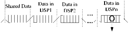
C. Data exchange among Memory blocks
In each parallel computation cycle, a data transmission sequence is to realize data exchange among different Memories. Data transmission sequence is composed of several IB cycles, and 32-bit data transmission is implemented in each IB cycle. As discussed above, the ADD signals in each IB cycle contain the definition of sender and receiver, so that it can set the data transmission sequence by setting IB address.
A Data Transmission Sequence
One IB Cycle
Fig.3 Data transmission sequence
Fig.3 demonstrates a data transmission sequence. The setting of the sequence depends on the actual data requirement among DSPs, and can be reconfigured by setting the relevant registers in IBMC. It is very important to downsize the sequence because it can significantly reduce the data transmission time, and meanwhile increase the ratio of data-sensitive computing in parallel cycle, which is indeed the efficiency of data transmission.
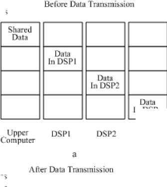
Memory before data exchange is shown in Fig.4 (a). Upper computer stores raw data (or parameters) as the shared data into locations at address of 0x0000 to 0x0ffff, and each DSP stores data that are to be shared into its private block. Fig 4 (b) shows the Memory status when all defined IB addresses are traversed and data transmission is completed. All data that are planned to be transmitted are shared by all DSPs without taking into account the specific need of a certain DSP. One potential problem is that, during data transmission, the access of DSP to its private block may lead to conflict on IB. Considering the strict timing requirement of IB, once the conflict happens, transmission failure will occur, which is undoubtedly unacceptable. Therefore, the DSP calculation is divided into data-sensitive and data-insensitive ones. In this way, the access conflict on IB is effectively avoided.
IB address
0x0000
Ox OftT YlxlM
Oxlfff
"0x2000
0х2ПГ
OxnOOO
Oxnfff
In DSPn
DSPn
IB address
|
0x0000 OxOftT |
Shared Data |
Shared Data |
Shared Data |
Shared Data |
|
thcliM Oxlfff |
Data n DSPl |
Data In DSPl |
Data In DSPl |
Data In DSPl |
|
Ux2.......... 0x2tfT |
Data n DSP2 |
Data In DSP2 |
Dara In DSP2 |
Data In DSP2 |
|
OxnOOO Oxnfff |
Data n DSPn |
Data In DSPn |
Data In DSPn |
Data In DSPn |
. I. pper Computer
DSP1 DSP2 DSPn
b
Fig.4 Memory before and after data transmission
-
D. Structure of IBSC and synchronous trigger
Fig.5 illustrates the structure of IBSC, and its functions are described as follow: (1) providing address decoding function for DSP to access DPRAM, which is implemented in EMIF_Adapter module; (2) realizing IB data transmission. After the IB address is validated, BTC (Bus Timing Controller) will determine whether the IBSC is a sender or receiver in the current IB cycle, and then switch the direction of data bus and provide control signals (Addr, AWEn, AOEn) to execute data sending or storage; (3) generating an interrupt signal for DSP to provide synchronous trigger, when a certain IB address is validated.
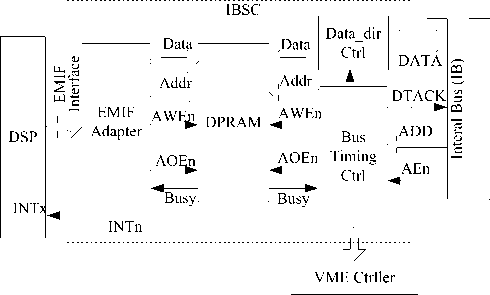
Fig.5. IBSC structure
Conflict caused by simultaneous memory location access can not be ignored. The common solution is “busy flag arbitration” provided by DPRAM, which can hold the later access until the end of the previous access. However, IB should have a higher priority to preempt the access of DSP because of the uninterruptible data transmission on IB. Therefore, the busy signal provided by DPRAM is not enough to exempt IB data transmission from conflict, and the solution to this problem is the strict scheme for Memory access of DSP, as discussed in section 2.
Synchronous trigger based on IB is an additional function for specific IB address. Each IBSC provides synchronous trigger for the associated DSP, and IB data broadcasting provides an excellent platform to make triggering with negligible synchronous error possible. The IB address of 0x0ffe (0x0fff) is chosen as the address for trigger 1 (2). IBSC monitors address lines, and BTC generates the INTn signals to interrupt DSP when the IB address matches the setting, as shown in Fig.5.
Two aspects of the trigger that need address are: (1) apparently trigger is controlled by IB address, so triggering time depends on configuration of data transmission sequence in IBMC. As introduced in section 2, the first and last addresses in the sequence are 0x0ffe and 0x0fff respectively, and thus trigger 1 and 2 are generated at the beginning and end of IB data transmission respectively; (2) Triggering timing is defined in IBSC by upper computer. Triggering timing requirement of DSP varies as clock frequency changes, so it is necessary to adjust the triggering timing during IBSC initiation to suit for different type of DSP in different clock frequency.
-
E. Structure of IBMC and mechanism of reconfiguration online
Fig.6 illustrates the structure of IBMC. Two types of data are transmitted to IBMC by upper computer via VME_Ctrller module - the contents for Addr_FIFO and configurations of IBMC_Regs. The defined IB addresses are stored in Addr_FIFO and every IB address corresponds to an IB cycle while all the IB cycles form the IB transmission sequence. During every execution of data transmission sequence, the defined IB addresses are outputted consecutively until FIFO is empty, then IB keeps idle until the next execution of sequence, as described in section 2. IBMC_Regs controls the actions of IBMC, including control of Addr_FIFO (enable or clear), definition of IB timing and a base-clock. Baseclock is the reference clock of the parallel cycle, and on its raising edge, data transmission sequence is activated and synchronous triggers occur alternatively. The baseclock frequency determines the time interval of parallel computation cycle, and this reference clock hidden in IB timing control offers "heartbeat" reference for the whole parallel computing architecture.
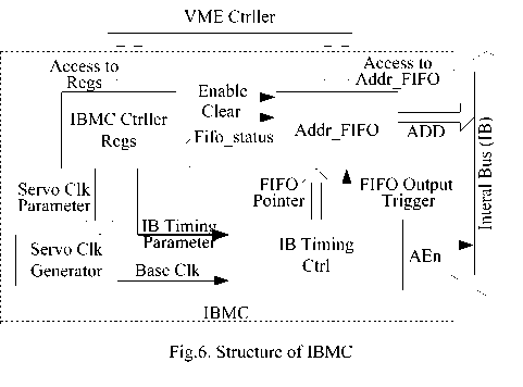
Details for IB are defined as registers in VME slave (IBMC), and upper computer can redefine the “behavior” of IB by configuring the IBMC online. The redefinition of Addr_FIFO makes it easy to provide new data transmission function online without changing hardware architecture even when the data exchange requirement changes. The redefinition of IB timing means transmission rate can be customized according to the need in actual application, if necessary, new type of device can be used on IB without suffering from compatibility problem. The redefinition of base-clock makes the computing cycle interval adjustable to provide reasonable size of time slot for different computing load. The flexibility brought by online reconfiguration is the main reason to adopt the scheme of user-defined internal bus, and FPDP is given up because of this as well. IBMC_Regs are listed in Table II.
TABLE II.
R egisters list in IBMC
|
Register Name |
Description |
|
IBMC_Control_Reg |
Definition of control signal to IBMC and its Addr_FIFO. |
|
IBMC_Status_Reg |
Current status of IBMC. magnetic induction |
|
IBMC_Err_Reg |
Error information. |
|
VME_INT_Control_Reg |
Setting for VME interrupts – interrupt enable, priority, and control. |
|
VME_INT_Vector_Reg |
Setting for interrupt vector. |
|
IB_Addr_FIFO_Reg |
Writing Addr_FIFO through this address. |
|
IB_Addr_Length_Reg |
Depth of Addr_FIFO, used to judge whether data transmission is over. |
|
IB_Timing_Reg |
Definition of IB timing. The setting is based on Internal global clock in IBMC as the minimum unit. |
|
BaseClk_Control_Reg |
Setting for base clock – enable, running cycle. |
|
BaseClk_Status_Reg |
Current status of base clock. |
IV. Data transmission model and analysis Template
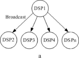
The model described in this section is only for data transmission on IB where only one transmission mode is involved, as shown in Fig.7 (a). DSP1 is the only source node, while other DSPs are destination nodes, and broadcast mode with single host and multi-slave are adopted. Fig.7 (b) illustrates the analysis of data transmission model.
In Data Transmission
Sers ice
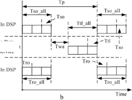
Fig.7. Data transmission model
TABLE III.
P arameters list in data transmission model
|
Parameter |
Description |
|
T p |
The length of time for one parallel computing cycle. |
|
T so _ all |
The length of time the sending processor is engaged in the data transmission in a parallel computing cycle; during this time the processor cannot perform other operations. |
|
T so |
The length of time the sending processor is engaged in the transmission of a 32-bit data. |
|
T wa |
The length of time spent in waiting execution of data transmission sequence. |
|
T tl |
The length of time spent in the transmission of a 32-bit data from sending to the receiving node. |
|
T tl _ all |
The length of total time spent in the transmission network from sending to the receiving node in a parallel computing cycle. |
|
T ro |
The length of time the receiving processor is engaged in the transmission of a 32-bit data. |
|
T ro _ all |
The length of time the receiving processor is engaged in the reception of data in a parallel computing cycle; during this time the processor cannot perform other operations. |
|
L d |
The size of data in transmission sequence, in word (32-bit), transmitted in a parallel computing cycle. |
|
K |
The ratio between T tl _ all and T p , which indicates the efficiency of data transmission function. |
|
N |
The number of processors in the parallel architecture. |
T tl _ all = L d X T tl
( 1 )
T total = T so all + T tl all + T ro all + T wa
= L d ( T so + T tl + T ro ) + T wa
K = L d X T tl / T p
( 2 )
( 3)
In formula 1, T tl is the transmission latency of single datum, in word (32 bit), and its stability only depends on the network transmission performance. Therefore, T tl _ all solely depends on L d and can be calculated accurately. In formula 2, T so and T ro are determined by EMIF Settings, and T wa indicates the total time spent on waiting for data transmission service. In formula 3, K indicates the efficiency of data transmission service, and the smaller it is, the less time spent on data transmission during the parallel computing cycle. The uncertainty of T total is mainly caused by DSP software plan ( T wa ), but not T tl _ all . In practical parallel servo computing, T tl _ all must be accurate and to small о Tn о .
proportion of p for the reason that partition of data-insensitive and data-sensitive computing is based on it. On the contrary, there is no high requirement for T total accuracy.
V. Experiment and result
The time parameters of IB timing mentioned in Fig. 2 are listed in table IV.
TABLE IV.
time parameters of IB timing
|
Parameter |
Value ( ns) |
Description |
||
|
Min |
Tpy |
Max |
||
|
t1 |
- |
20 |
- |
ADD[15:0] valid before AEn valid |
|
t2 |
0 |
10 |
20 |
AEn valid to DATA[31:0] valid |
|
t3 |
10 |
10 |
20 |
DATA[31:0] valid to DTACK valid |
|
t4 |
20 |
20 |
30 |
DTACK low pluse |
|
t5 |
- |
10 |
- |
DTACK invalid to DATA[31:0] high impedance |
|
t6 |
0 |
20 |
20 |
DATA[31:0] high impedance to AEn remains valid |
|
t7 |
10 |
10 |
30 |
ADD[15:0] remain valid after AEn invalid |
Fig.8 (a) plots T tl _ all with respect to L d using results from experiment with ( N =6). Indicators of the goodness of the fit are: SSE ( sum of squared error ) =1.19e-005, RMSE ( root mean square error ) =0.001992, R-square= 1. From the plot, it is not difficult to see that the linear dependency of T tl _ all on L d is almost perfect.
Fig.8 (b) plots the value of T tl obtained from experiment. The error is of sub-nanosecond scale, and the major part of it is caused by non-uniformity of signal transmission characteristics in IB backplane and internal reference clock jitter in IBMC. According to the experimental results, T tl is accurate enough, so that the T tl _ all and K can be both calculated accurately using the value of L d .
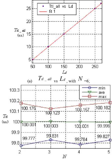
( b ) T tl vs N
Fig.8. Performance of IB data transmission
VI. Conclusion
Communication service proposed in this paper is based on standard VME bus and Internal Bus (IB) in P2, which provided high-performance data transmission and precise synchronization trigger support for the processors involved in parallel computing. Several conclusions can be drawn from preceding discussion and analysis of experimental result. (1) The maximum number of processors is 15 in the communication service. It can be increased to 19 by modifying the IB protocol, and the ceiling is 19 because there are only 21 slots in standard
VME rack while two of them are occupied by upper computer and IBMC. (2) The stable achieved bandwidth in communication is 10M *32bit/S, and it can be increased significantly by improving signal transmission characteristics in IB backplane. (3) The data transmission latency error is of sub-nanosecond scale and synchronization error is of nanosecond scale, both of which are not affected by the number of processors. (4) In practical application, time spent on data transmission is only 6.575% in every parallel computing cycle.
However, the assumption, on which the communication service is built, is that the data transmission need is clearly specified - only one data transmission sequence with static source and destination addresses is needed in every parallel computing cycle. The over-simplified assumption undermines its universal applicability to most parallel computing architectures. What’s more, limited by the number of the number of slots in the standard VME rack, it’s impossible for it to support more processors.
Future research would focus on the following two aspects: (1) Improving the universal applicability of communication service. The design of a strict and precise multi-layer communication model based on high-speed serial link is a potential solution. However, the transmission model must be strict and precise, and the communication protocol must avoid the factors such as handshaking, unfixed routing, data congestion .etc, which cause the uncertainty of communication performance. We are developing the research of precise synchronization based on high-speed fiber channel right now. (2) Implementation of high performance communication in multi VME racks. If the number of processors exceeds 19, right now we can not implement communication service discussed.
Acknowledgment
References A High-Performance Communication Service for Parallel Servo Computing
- Fujita Itaru, Sakai Fumio, Uzawa Shigeyuki, Next generation scanner to sub-100 nm lithography, In Proceedings of SPIE. Santa Clara, CA, USA, 2003, pp. 811-821.
- Yang Liangliang, Zhou Yunfei, Pan Haihong, Luo Fuyuan. Research on synchronous mechanism of step-scan projection lithography, China mechanical engineering, 2009(20), pp. 20-23, 43.
- Wang Chunhong, Hu Jinchun, Zhu Yu, Yin Wensheng, Optimal synchronous trajectory tracking control of wafer and reticle stages. Tsinghua Science and Technology, 2009 (14), pp. 287-292.
- Message Passing Interface Forum, MPI: A Message-Passing Interface Standard, Technical Report CS-94-230,Computer Science Department, University of Tennessee, 1994.
- J. Bruck, D. Dolev, C. Ho, M. Rosu, R. Strong, Efficient message passing interface (MPI) for parallel computing on clusters of workstations, Journal of Parallel and Distributed Computing, 1997(40), pp. 19- 34.
- M. Lauria, A. Chien, MPI-FM: High performance MPI on workstation clusters, Journal of Parallel and Distributed Computing, 1997(40), pp. 4-18.
- W. Gropp, E. Lusk, N. Doss, A. Skjellum, A high-performance, portable implementation of the MPI message passing interface standard, Parallel Computing, 1996(22), pp. 89- 828.
- R. Hempel, D.W. Walker, The emergence of the MPI message passing standard for parallel computing, Computer Standards & Interfaces, 1999(21), pp. 51- 62.
- TMS320C6713B floating-point digital signal processor, http://focus.ti.com.cn/cn/docs/prod/folders/print/tms320c6713b.html
- Yan Luxin , Zhang Tianxu , Zhong sheng, Parallel system architecture of multi-DSP interconnected by FPGA, Systems Engineering and Electronics, 2005 (27), pp. 1757-1759, 1775.
- James Kohout, Alan D. George, A high-performance communication service for parallel computing on distributed DSP systems, Parallel Computing, 2003(29), pp. 851- 878.
- Bai Yucheng, Tang Xiaoqi, Chen Jihong, Hu Huan, Research on multi-axis synchronous control for network CNC system, manufacturing technology & machine tool , 2008 (8), pp. 61-65.
- Justin (Gus) Hurwitz, Wu-chun Feng, Analyzing MPI performance over 10-Gigabit Ethernet, Journal of parallel and distributed computing, 2005(65), pp. 1253-1260.
- Amit Karwande, XinYuan, DavidK. Lowenthal, An MPI prototype for compiled communication on Ethernet switched clusters, Journal of parallel and distributed computing, 2005(65), pp. 1123-1133.
- U.S. VMEbus International Trade Association. American National Standard for Front Panel Data Port Specifications. U.S. Scottsdale. 1998
- Zhang Huachun, Sun Changyu, A New Design Method for High-Speed Data Acquisition System Based on FPDP, Systems Engineering and Electronics, 2003(25), pp. 787-789, 803.
- Zhao Chunhui, Yang Shuyuan, Yuan Jianping, Design of DSP-specific VME-64 bus interface of NUMA multi-processors systems, Systems Engineering and Electronics 2005 (27), pp. 189-192.
