A Low Power BIST TPG for High Fault Coverage

Author: R.Varatharajan, Lekha R.
Journal: International Journal of Information Engineering and Electronic Business(IJIEEB) @ijieeb
Article in issue: 4 vol.4, 2012.
Free access
A low hardware overhead scan based BIST test pattern generator (TPG) that reduces switching activities in circuit under test (CUTs) and also achieve very high fault coverage with reasonable length of test sequence is proposed. When the proposed TPG used to generate test patterns for test-per-scan BIST, it decreases the number transitions that occur during scan shifting and hence reduces the switching activity in the CUT. The proposed TPG does not require modifying the function logic and does not degrade system performance. The proposed BIST comprised of three TPGs: Low transition random TPG (LT-RTPG), 3-weight weighted random BIST (3-weight ERBIST) and Dual-speed LFSR (DS-LFSR). Test patterns generated by the LT-RTPG detect the easy-to-detect faults and remain the undetected faults can be detected by the WRBIST. The 3-weight WRBIST is used to reduce the test sequence lengths by improving detection probabilities of random pattern resistant faults (RPRF). The DS-LFSR consists of two LFSR's, slow LFSR and normal–speed LFSR. The DS-LFSR lowers the transition density at their circuit inputs.
Built-in self-test (BIST), switching activity, low power testing, test pattern generator
Short address: https://sciup.org/15013134
IDR: 15013134
Text of the scientific article A Low Power BIST TPG for High Fault Coverage
Published Online August 2012 in MECS
Modern design and package technologies make external testing increasingly difficult and the Built-in Self-test (BIST) has emerged as a promising solution to the VLSI testing problem. BIST is a design for testability methodology aimed at detecting faulty components in a system by incorporating test logic on-chip. The main components of a BIST scheme[1] are the test pattern generator (TPG), the response compactor, and the signature analyzer. Among various BIST schemes, pseudo random BIST is most widely used since it is most economical. Unlike deterministic stored pattern BIST, which requires the high hardware overhead due to the memory devices required to store precomputed test patterns, pseudorandom BIST , where test patterns are generated by pseudo random pattern generators such linear feedback shift registers (LFSRs) and cellular automata (CA), requires very little hardware overhead. However, BIST using only pseudo random patterns doesn’t provide high fault coverage due to the existence of random pattern resistant faults (RPRF).
Several techniques have been suggested for enhancing the fault coverage achieved with BIST. These techniques can be classified as: (1) Mixed-mode testing where the circuit is tested in II phases. In the first phase, pseudo-random patterns are applied. In the second, deterministic patterns are applied to target the undetected faults. Storing deterministic patterns in a ROM requires a large amount of hardware overhead. (2) Modifying the circuit under test by test point insertion or by redesigning the CUT to improve the fault detection probabilities. The drawback of these techniques is that they generally add extra levels of logic to the circuit that can degrade system performance. (3) Weighted pseudo-random patterns , where the random patterns are biased using extra logic to increase the probability of detecting RPRFs. In weighted random pattern testing, the outputs of TPG are biased to generate test sequences that have nonuniform signal probabilities to increase detection probabilities of RPRFs that escape pseudorandom test sequences, which have a uniform signal probability of 0.5.
A 3-weight WRBIST can be classified as an extreme case of conventional weighted random pattern testing BIST. However, in contrast to conventional weighted random pattern testing BIST where various weights, e.g., 0, 0.25, 0.5, 0.75, 1.0, can be assigned to outputs of TPGs, in 3-weight WRBIST, only three weights, 0, 0.5, and 1, are assigned. Since only three weights are used, circuitry to generate weights is simple; weight 1 (0) is obtained by fixing a signal to a 1 (0) and weight 0.5 by driving a signal by an output of a pseudorandom pattern generator, such as an LFSR. Though the attainment of high fault coverage with practical lengths of test sequences is still one concern of BIST techniques, reducing switching activity (SA) has become another important objective. It has been observed that SA during test application is often significantly higher than that during normal operation. The correlation between consecutive random patterns generated by an LFSR is low; this is a well-known property of LFSR generated patterns [6]. On the other hand, significant correlation exists between consecutive patterns during the normal operation of a circuit.
Since heat dissipation in a CMOS circuit is proportional to switching activity, a CUT can be permanently damaged due to excessive heat dissipation if SA in the circuit during test application is much higher than that during its normal operation.
BIST schemes can be classified into (a) test-per-clock (b) test-per-scan, according to the way of applying the test patterns to the CUT. In test-per-clock BIST, the outputs of TPGs are directly connected to the inputs of the CUT and new test pattern is applied to the inputs of the CUT at every clock. In test-per-scan BIST, a test pattern is applied to a CUT every m+1 cycles, where m is the number of flip-flops in a scan chain [4].
The rest of this paper is organized as follows. The techniques that are used in this paper to reduce switching activity during BIST are illustrated in Section III. Section IV and V briefly introduces the serial fixing 3-weight WRBIST and DS-LFSR. The architecture of the proposed TPG and the outline of algorithm used to design the proposed BIST TPG are described in Section VI. Finally, Section VII presents the conclusions.
-
II. BACKGROUND
In this paper, we assume that the sequential circuit has n primary and m state inputs, implemented in CMOS, has full scan, and employs scan based BIST to apply test patterns and observe responses. A test pattern for state inputs, which is generated by a TPG, is scanned into a scan chain for m cycles by repeated scan shift operations and the response to the applied test pattern is captured into the scan chain in the next cycle. We also assume that unlike state inputs, for which test patterns are applied o the CUT via the full-scan chain by a sequence of scan shift operations, test patterns for primary inputs are applied to the CUT every m+1 cycles from a TPG whose outputs are directly connected to primary inputs or through a boundary scan chain whose outputs are updated every m + 1 cycles. Hence, most SA in CUTs that have long scan chains, i.e., m >> 1, is caused by transition at scan inputs during scan shift operations. This will increase test application time by about a factor of d if scan flipflops are clocked at 1/d speed during scan shift operations. Furthermore, reducing test clock speed doesn’t solve high power/ground noise problem that is caused by a large number of simultaneous transitions. A transition at the scan chain input at a scan shift cycle t, which is caused by scanning in a value that is opposite to the value that was scanned in at the previous scan shift cycle t-1, continuously causes transitions at scan inputs while the travels through the scan chain during the following scan shift cycles. Fig. 1 shows scan shift operations for a scan chain that has 5 scan flip-flops. ince a 0 is scanned into the scan chain at time t = 0, the 1 that is scanned the scan chain at time t = 1 causes a transition at the scan chain input and continuously causes transitions at scan flip-flops it passes through until it arrives at its final destination at time t =5. On the other hand, the next 1, which is scanned into the scan chain at time t = 2, causes no transitions at the scan chain input and arrives at its final destination at time t=5 without causing any transition at scan flip-flops it passes through. This shows that transition that occurs at the entire scan chain can be reduced by reducing transitions at the scan chain input.
Chain p 0 p 1 p 2 p 3 p 4 Chai
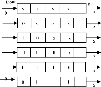
Fig: 1 Transitions at scan chain
-
III. LOW TRANSITION RTPG
-
A. Analysis of LT-RTPG
The combinational part of a sequential circuit can be viewed a collection of output cones, where an output cone Ω is composed of all the logic and inputs (primary and state) that form the fan-in of jth output. A pair of inputs are said to be compatible if there exists no circuit cone to which they both belong. Any correlation between the values applied to a pair of compatible inputs does not reduce the fault coverage for any given test length for faults such as stuck-at. Consider a full scan circuit with a single scan chain. Let the span S j of cone Ω be the distance between first and last flip-flops in the scan chain [2], whose outputs drive the state inputs of the cone. If the α -th and β -th flip-flops of the
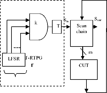
Fig.2. Low Transition RTPG scan chain drive the first and last flip-flops of the Ω , then Sj = β- α + 1 , then span S of the circuit is defined as the maximum of spans of all its cones. For the above type of faults, it is sufficient to apply all possible patterns to each set of S consecutive flip-flops of the scan chain to guarantee coverage of all faults [4].
-
B. Architecture of LT-RTPG design
The LT-RTPG reduces SA during BIST by reducing transitions at scan flip-flops during scan shift operations. Fig.2 shows an architecture called LT-RTPG. The LT-RTPG is comprised of an r-stage
LFSR, a k-input AND gate, and a T flip-flop. Hence, it can be implemented with very little hardware. We assume that every LFSR stage Di, where i=1, 2… r, has a normal as well as an inverted output, Q andQ , respectively. The normal (inverted) output of a stage Di of the LFSR, Q (Q ), is said to have inversion parity of 0(1). Each of K inputs of the AND gate is connected to either a normal or an inverting output of the LFSR stages. If an output of an LFSR stage is connected to an input of the AND gate, the stage is said to have been tapped. The tap configuration of the TPG, TC = {Q1*, Q2*,.. Qx*}, where Qx*= Qx or Qi and x=1,2,…,k, denotes a set of tapped stages of the LFSR and the inversion parities of the outputs of the stages tapped. The output of the AND gate is connected to the T-FF. Finally, the output of the T-FF is connected to the scan chain. If large K is used, large sets of neighboring state inputs will be assigned identical values in most test patterns, resulting in the decrease fault coverage or the increase in test sequence length. Hence, LT-RTPGs with only K=2 or 3 are used. Since a T flip- flop holds previous values until the input of the T flip-flop is assigned a 1, the same value v, where v ∈ {0,1}, is repeatedly scanned into the scan chain until the value at the output of the AND gate becomes 1.
-
IV. 3-WEIGHT WEIGHTED RANDOM BIST
-
A. Generators
In 3-weight WRBIST, detection probabilities of RPRFs are improved by fixing part of inputs of the CUT to binary values specified in test cubes for targeted RPRFs. A test cube for a fault is a test that has unspecified inputs and the detection probability of a fault is defined as the probability that a randomly generated vector detects the fault. A generator or a weight set is a vector that conveys information on inputs to be fixed and values to which these inputs are to fixed during 3-weight Weighted random BIST. C= { c0, c1,^,^1"1 } are the set of test cubes for RPRFs in a CUT, where c j ={ c j , c j ,..., c j } is an m -bit test , 0 , 1 ,, m - 1
cube and where m is the number of inputs of the CUT, cj ∈ {0,1,X} ∀i , where X is a don’t care. Generator of the BIST gen(C)={g0,g1,^,gm"1} is denoted as an m-bit tuple where gk ∈ {0,1,X,U} (k=0,1,…,m-1), m is the number of inputs, and gk is defined as follows.
-
1 if c j =1 or x in ∀ c j ∈ c and at least one ckj =1,
gk = 0 if c j =0 or x in ∀c j ∈ c and at least one c j =1,
U if ∃ ca =1 and cb =0, where ca,c b ∈ C,
X otherwise.
(i)
When input pk that is assigned a 1 (0) in the generator, fixing to a 1 (0) improves detection probabilities of faults that require a 1 (0) at input p k to be detected by a factor of 2. On the other hand, fixing inputs that assigned a U in the generator to a binary value 0 or 1 may make some faults undetectable. Since those inputs are assigned 1 in some test cube(s) and 0 in other test cube(s). If a circuit contains a large number of RPRFs, then test cubes for RPRFs may be assigned opposite values in many inputs resulting in a generator where most inputs are assigned U ’s. Only a few inputs can be fixed in such generators without making any faults untestable. Hence, if a circuit has a large number of RPRFs, then multiple generators, each of which is calculated from test cubes for a subset of RPRFs in the circuit, may be required to achieve high fault
|
C |
p 5 p 4 p 3 p 2 p 1 p 0 |
F dp |
|
2 c |
c0 1 X 1 0 X 0 c1 0 1 X 0 1 0 1 1 1 X X 1 |
f0 1/24 f1 1/25 f2 1/24 |
|
3 c |
X X 0 X 1 1 |
f3 1/23 |
|
gen(C) |
U 1 U 0 1 U |
Fig.3. Example test cube set C
C0 p 5 p 4 p 3 p 2 p 1 p 0 C1 p 5 p 4 p 3 p 2 p 1 p 0
c0 1 X 1 0 X 0 c2 1 1 1 X X 1
c1 0 1 X 0 1 0 c3 X X 0 X 1 1
g(C0) U 1 1 0 1 0 g(C0) 1 1 U X 1 1
Fig.4. Example test cube subsets C0, C1
|
Gen(C0) |
1 |
U |
X |
X |
X |
U |
1 |
X |
0 |
|
Gen(C1) |
1 |
0 |
U |
1 |
0 |
U |
1 |
0 |
0 |
|
Gen(C2) |
0 |
0 |
X |
X |
X |
U |
0 |
1 |
1 |
Fig.5. Example generators (weight sets)
coverage with a reasonable length of random pattern sequence. Fig. 5 shows an example of 3 generators for a circuit that has 8 inputs
-
B. Architecture of 3-weight WRBIST
Two different scan based 3-weight WRBIST scheme proposed in [10] are serial fixing and parallel fixing 3-weight WRBIST. However, in this paper, the serial fixing 3-weight WRBIST is exclusively used because it has the property to reduce transitions at scan inputs during scan shift operations. The low transition property of the serial fixing 3-weight WRBIST is described in [10]. Fig 6 shows the implementation of a serial fixing 3-weight WRBIST for the generator shown in Fig 5. The scan counter is an ( m+ 1) modulo counter, where m is the number of scan elements in the scan chain. When the content of the generator counter is k, a value for input p k is scanned to the scan chain input. The generator counter selects appropriate generators; if the content of the generator counter is i , generator gen ( C i ) is selected to generate T i 3-weight WRBIST patterns. Pseudo random pattern sequence generated by the LFSR are fixed by controlling the gates, AND & OR, with overriding signals s 0 and s 1 ; fixing a random value to a 0 is achieved by setting s 0 to a 1and s 1 to a 0 and fixing a random value to a 1 is achieved by setting s 1 to a 1. Since a random value can be fixed to a 1by setting s 1 to a 1 independent of the state of s 0 , the state of s 0 is a don’t-care when fixing a random value to a 1. The outputs of the decoding logic [3], D 0 and D 1 , are generated by the outputs of
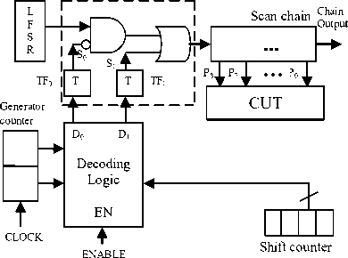
Fig.6. Architecture of 3-weight WRBIST the scan counter and the generator counter as inputs. T flip-flop TF0 (TF1) toggles its state when the output of the decoding logic D0 (D1) is assigned a 1. In consequence, the on-set of the function for the decoding logic lists the contents of the generator and scan counter at test cycles when TF0 and/or TF1 require toggling. The scan counter is required by all scan-based BIST schemes and is not particular to the proposed BIST scheme. All BIST controllers also need a vector counter that counts the number of test patterns applied.
The generator counter can be implemented with [log2m] MSB stages of the existing vector counter, where m is the number of generators. Hence, no additional hardware is required for the generator counter, either. Hence, hardware over- head for implementing a 3-weight WRBIST is incurred only by the decoding logic and fixing logic, which includes the two T flip-flop and AND and OR gates. In [10], in order to minimize hardware overhead for the decoding logic, the number of minterms in the on-set (or off-set) of the function for the decoding logic is minimized. This is achieved by ordering scan chains such that the number of toggles at TF0 and TF1 required to scan in appropriate values for scan inputs, which are specified in generators, is minimized. In order to minimize the number of toggles required at T flip- flops TF0 and TF1, Inputs that are assigned the same values in most generators are placed in neighbor in the same chain by the scan ordering procedure. These pairs of inputs are placed in neighbors to minimize toggles required at the T flipflops.
-
V. DUAL SPEED LFSR
Dual-Speed LFSR (DS-LFSR) TPG consists of two LFSRs, a slow LFSR is driven by a slow clock and normal speed LFSR. The use of DS-LFSR lowers the transition density at the circuit input driven by slow LFSR, leading to a reduction in heat dissipation during test application with slight area over head. Dual Strategy is employed to reduce both Average and Peak power [5]. The slow LFSR is driven by a slow clock whose speed is l/dth that of the normal clock which drives the normal-speed LFSR. The DS-LFSR is designed in such a way that the generated patterns are all unique and uniformly distributed to achieve high fault coverage. Fig. 7 shows a BIST architecture which is equipped with a slow and a normal-speed LFSR. The empirical analysis using x2 tests demonstrates that the DS-LFSR generated sequences are more uniformly distributed than the sequences generated by single LFSR’s with primitive feedback polynomials. The slow speed LFSR will be clocked by a clock whose frequency is l/dth of that of the normal clock i.e. slow clock speed = normal clock speed/d. (To simplify the following discussions well as the hardware, d will be assumed to be a power of 2) Note that the slow LFSR has both slow clock and normal clock as clock inputs and has a control signal select clock which selects either slow clock or clock. Slow clock is selected when the slow LFSR is used as a test pattern generator; CLK is used when the CUT is in the normal mode or the slow LFSR functions as a multiple input signature register (MISR).
-
VI. PROPOSED LOW POWER BIST TPG
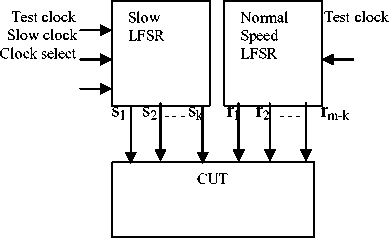
Fig. 7 Architecture DS-LFSR
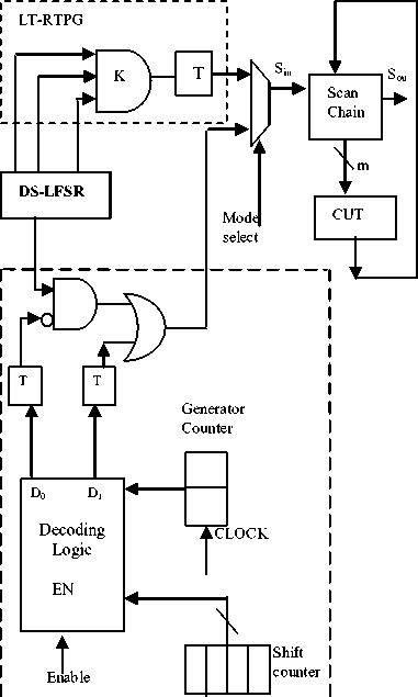
Fig.8. Architecture of the proposed BIST different BIST sessions; the LT-RTPG and WRBIST session. In the first test session, test patterns generated by the LT-RTPG are selected and scanned into the scan chain to detect the easy to detect faults. In the second session, test pattern generated by the 3-weight WRBISTare selected to detect the faults that remain undetected after the first session. Considering the fact that an LT-RTPG is implemented with very little hardware overhead (only y T flip-flops and y AND gates in addition to an DS-LFSR), overall hardware overhead to implement the proposed TPG is determined by hardware overhead for the decoding logic of the 3-weight WRBIST TPG. The y multiplexers that drive scan chain inputs select test sequence to be scanned into the scan chains; when the mode select signal, which selects inputs of all y multiplexers, is set to a 0, test patterns generated by the LT-RTPG are selected and when the mode select signal is to set to 1, test patterns generated by the 3-weight WRBIST TPG are selected. The test patterns generated by the LT-RTPG are applied to the CUT until no new faults are detected for a predetermined period. The faults that remain undetected by test patterns generated by the LT-RTPG are considered RPRFs and later targeted by test patterns generated by the 3-weight WRBIST TPG [11].
-
VII. CONCLUSION
This paper proposes and presents a low hardware overhead test pattern generator (TPG) for a scan based BIST that can reduce SA in CUTs during BIST and also achieve very high fault coverage with a reasonable length of test sequence.
References A Low Power BIST TPG for High Fault Coverage
- Seongmoon Wang, "A BIST TPG for Low Power Dissipation and High Fault Coverage", IEEE TRANSACTIONSON VLSI SYSTEMS, VOL.15,NO.7,JULY2007.
- Malav Shah and Dipankar Nag choudhuri, "BIST Scheme for Low Heat Dissipation and Reduced Test Application Time" 2006 IFIP.
- S.Wang and S.K.Gupta,LT-RTPG: A New Test-Per-Scan BIST TPG for Low Switching Activity, IEEE Trans.CAD.Integr. Circuits Syst., vol.25,no.8,pp.1565-1574,Aug.2006.
- Jiann-Chyi Rau, Ying-Fu Ho and Po-Han Wu, "A Novel Reseeding Mechanism for Pseudo Random testing of VLSI circuits", IEEE 2005.
- Chaowen Yu, Sudhakar M. Reddy and Irith Pomeran "Circuit Independent Weighted Pseudo-Random BIST Pattern Generator", 14th ATS symposium, IEEE2005.
- Chun-Yi Lee and Chien-Mo Li, " Segment Weighted Random BIST (SWR-BIST): A Low Power BIST Technique", IEEE2005.
- Chaowen Yu, Sudhakar M. Reddy and Irith Pomeranz, "Weighted Pseudo-Random BIST for N-detection of Single Stuck-at Faults", 13th ATS symposium, IEEE2004.
- N.Z.Basturkmen,S.M.Reddy,and I.Pomeranz, A low power pseudo-random BIST technique, Proceedings of 8th IEEE International On-LineTesting Workshop (IOLTW'02), IEEE2002.
- Seongmoon Wang, Sandeep K. Gupta, "DS-LFSR: A New BIST TPG for Low Heat Dissip- ation", International Test Conference, IEEE1997.
- Seongmoon Wang, "Low Hardware Overhead Scan Based 3-Weight Weighted Random BIST", ITC, IEEE1997.
- Parag K.Lala,"Digital Circuit Testing and Testability".
