A New Adder Theory Based on Half Adder and Implementation in CMOS Gates

Author: Zhanfeng Zhang, Liyuan Sheng, Wenming Jiang, Shuai Tong, Hua Cao
Journal: International Journal of Image, Graphics and Signal Processing(IJIGSP) @ijigsp
Article in issue: 2 vol.2, 2010.
Free access
This paper proposes a new theory of adder and its basic structure. The new adder of asynchronous structure constructed by half adders, called Parallel Feedback Carry Adder (PFCA) as its carry mode is parallel feedback. In theory, the area consumption of n-bit PFCA is close to O(n) and the average length of carry chain is O(log n). A CMOS gate implementation scheme is implemented. HSPICE simulation results show that PFCA has obvious advantages over RCA, CLA, CSeA in speed and area, especially when n is bigger.
Half adder trigger, parallel feedback carry adder, CMOS gate
Short address: https://sciup.org/15012034
IDR: 15012034
Text of the scientific article A New Adder Theory Based on Half Adder and Implementation in CMOS Gates
Published Online December 2010 in MECS
As a basic computation function of data processing, integer addition is th e most commonly used and important operation in digital circuit design. Therefore the speed and area consumption of adders have great impact on the overall system speed and scale.
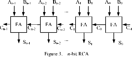
A ripple-carry adder[1] is implemented by using multiple copies of a 1 -bit full adder, where the carry out of the ( i - 1 )-th full adder is fed into the carry input of the i -th full adder and the lowest order full adder has a carry input of 0 . The carries must ripple from the least-significant bit to the most-significant bit, resulting in an addition time of O ( n )( n is the word length of the adder). Obviously the ripple-carry adder scheme is very slow for building a wide adder while area consumption is very small.
To speed up adders, a wide variety of techniques have been proposed. These techniques include synchronous adders, such as: Con dition Carry Adder (CCA), Carry Look ahead Adder (CLA), Ling Adder, Manchester Carry Chain Adder, Conventional Carry Skip Adder(CCSKA), Modified Carry Skip Adder, Carry Select Adder (CSeA), Carry Save Adder(CSA)[2~4]; And asynchronous adders , such as: C arry Completion Sensing Adder(CCSA), Delay Insensitive Carry Look ahead Adder(DICLA), Speed-up DICLA[5~6]. These synchronous adder circuits operate at the worst rates, wh ile asynchronous ones operate only at average rates. The adders motioned above are all constructed by full adders despite they have different structures. In general, one adder has the smallest area consumption; it cannot reach the fastest speed. As a result, area-time efficiency is proposed to evaluate the performance of various adders, the smaller the product of area and computation time, the better area-time efficiency is.
This paper proposes a new adder theory and its structure, which is constructed by half adders. In theory, this adder has the area asymptotic requirement O ( n ) and average computation time O (log n ). It shows that the area of PFCA is no t larger than RCA and its sp eed is not slower than CLA. Because full adder consists of two half adder and one OR gate, PFCA provides more than 4 times space for increasing the area-time efficiency in both area and speed. An implementation of PFCA based on CMOS gate is pro vided to verify this theory. HSPICE simulation results show that PFCA has obvious advantage over RCA, CLA, CSeA in speed and area, showing potential applications especially when word length is longer.
-
II. PFCA Theory
-
A . Basic Unit of Adders
Let A and B be two n -bit binary numbers, as follows:
fA = A A la A- l AAA n-1 n-2i
,
[ B = B n - 1 B n - 2 L B , L B 2 BB 0
Let S be their sum:
S = A + B = Sn-I ...SiLS2SiSo,(2)
Where A i and B i are the i -th bit of A and B .
f S = A ,, e Bs e cs_a
I i i i i 1 ,
C = At ■ Bt + (At e Bt) ■ ciX i i i i ii
Where C - 1 = 0 . Formula (3) a re the full adder expression, structure and simplified symbol of full adder are shown in Fig. 1(a) and Fig. 1(b). From Fig. 1(a), we know that a full adder is consisted of two AND gates, two XOR gates and one OR gate.
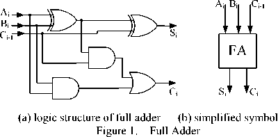
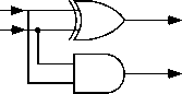
A half adder consists of one AND gate and one XOR gate (shown in Fig.2). From the perspective of l ogic gates, one full adder consists of two half adders and one OR gate.
A B
S
C
(a) logic structure of half adder
Figure 2. Half Adder
(b) simplified symbol
Half adder has carry-output but no carry-input. As a result, all existing adders are based on full adder and a n -bit adder needs n full adders at least. A good e xample is that an n -bit RCA (shown in Fig. 3) needs n full adders, and its area co nsumption is the least wh ile requiring a long computation time.
B Theory and Basic Structure of PFCA
A new structure s hould be extracted from the basic structure of adders shown in equation (2) and equation (3) in order to implement n -bit adder based on half adder. Let A and B be two n -bit binary numbers, the superscript be the time variable of iteration times, the subscript be the order in the binary number. Then A k , Bk is the value of A and B after k iterative operations.
A k = A k - 1 l A ik l AXA o k , k = 0,1,2, l , (4)
Bk = B^ L B i L B№ 0 , k = 0,1,2, L , (5)
Obviously, the initial value is:
0 0 0 000
A A A n - 1 A i A 2 A 1 A 0
B 0 = B = B ° - 1 ••• B i B 2 B 1 0 B 0 . n is the word length of
A and B .
Let S i k and C i k be the sum bit and carry bit of A, B; which are also in termediate variables of iteration. They are as follows:
S i = A i - 1 © B i - 1 , i = 0,1,2, L , n ; k = 1, L (6)
C i = A i - 1 • B i - 1 , i = 0,1,2, l , n ; k = 1, l ,(7)
When a fee dback mechanism is b rought in, let
A i = S i , i = 0,1,2, l , n ; k = 1,2, l , (8)
B i = C i - 1 , i = 0,1,2, L , n ; k = 1,2, L , (9)
where C-1 = 0 , Si and Ci-1 constitute a n ew group of Ak and Bk , and they return to equation (4) and equation (5), then operation repeats from equation (4) and equation (5) to equation (8) and equation (9). The ideal structure of PFC A is sho wn in Fig. 4. Si (i = 0,1,2, l, n — 1) are not allowed connect to Ai (i = 0,1,2, l , n — 1) directly in digital design (the dotted line).
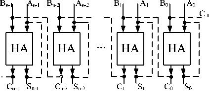
Figure 4. The basic structure of PFCA based on HA
An ideal n -bit PFCA can be drawn out by cascading n units of this kind and its basic structure is shown in Fig. 4. The area asymptotic requirement of PFCA is O ( n ) and all the half adders will complete their operations in each iterating, then the results are feedback to the inputs for next operations. Therefore, PFCA is a parallel adder with feedback. Compared to all existing adders, PFCA has less time computation and sm aller area and its area -time efficiency can be increased 4 times because of t he two advantages of PFCA: 1. parallel mode, which speeds up the circuits of adder; 2. feedback mode, which increases the number of the basic units used.
Theorem 1. If C i = 0 , i = 0,1,2, l , n — 1 , then the sum S of A and B satisfies:
S = A + B = A k (10)
The theorem can be easily proved. Equation (6) generates one new addend:
S i = A k - 1 © Bk - 1 ,( k = 1,2, L ).
Equation (7) generates the other new addend : C i = A i - 1 • B i - 1 ,( k = 1,2, l ). As feedback mechanism brought in, the next add operation will be: S i + C i ,( k = 1,2, l ). Then the final sum will be got after many times of iteration until the carry-bits are all zero.
C . The Analysis of Properties in the Basic Unit of PFCA
A basic unit extracted from Fig. 4 is shown in Fig. 5 (the dotted lines stand for this type of feedbacks are not allowed in digital design)and called half adder trigger. Output S feedback to input A., The input B is trigger port and the output C , A(or S) are status ports.
BA

HA
Figure 5. The half adder trigger
-
i) .If B = 0 , then S = B © A = A , C = 0 all the time. Thus, the status of port A stays and the half adder trigger has the function of memorizer;
-
ii) .If B = 1 , S = B © A = A , C = A ■ B = A and the status changes all the time. The status of port S is reverse to that of port A , forming negative feedback in the external of HA and the delay time for transporting signals from A to S is denoted as T HA in the internal of half adder. Therefore, the half adder trigger will form “0-1” self-oscillation loop with its oscillation period T HA , which can be used as local clock. The curve of C is the same as the A , but there is some delay.
-
D . The PFCA Theory Validation
PFCA is an asynchronous adder, so we can use average computation time instead of the speed of PFCA. The average computation time is decided by the average length of carry chain. Necessary and sufficient conditions of carry chain existing is as follows:
There must be a natural number m meet the equation: (AB )(AM © BM) l (A^m © B^m) = 1, i = 0,1, l n - 1. Then the carry chain can be expressed by: l = m + 1.
If there is no carry chain, l = 0. Generally speaking, there may be se veral carry chai ns for different input combination. Let l' be the longest carry chain of input combinations, we can c ompute the average length of carry chain for these input combinations by:
l =
i = 22"
z l'
i = 1
2 2 n
The occupied area of n -bit PFCA is close to O ( n )( as we can easily get in the Fig. 4). The average length of carry chain in n -bit asynchronous adder is O (log n )[7~13] . We prove this by statistical method, Table1 and Fig. 6 are the statistics data.
Table I
The data of statistics in PFCA
|
bits |
total number of addition |
total number of iteration |
average number of iteration |
|
1 |
2 2 |
2 |
0.5 |
|
2 |
24 |
16 |
1.0 |
|
3 |
2 6 |
92 |
1.4375 |
|
4 |
2 8 |
464 |
1.8125 |
|
5 |
2 10 |
2188 |
2.1367 |
|
6 |
2 12 |
9900 |
2.4170 |
|
7 |
214 |
43612 |
2.6619 |
|
8 |
2 16 |
188548 |
2.8770 |
|
9 |
2 18 |
804220 |
3.0679 |
|
10 |
2 20 |
3395732 |
3.2384 |
|
11 |
2 22 |
14227548 |
3.3921 |
|
12 |
224 |
59250388 |
3.5316 |
|
13 |
2 26 |
245556540 |
3.6591 |
|
14 |
2 28 |
1013694772 |
3.7763 |
|
15 |
2 30 |
4171200028 |
3.8847 |
|
16 |
2 32 |
17117734228 |
3.9855 |
|
17 |
234 |
70088425212 |
4.0797 |
|
18 |
2 36 |
2864222399880 |
4.16799 |
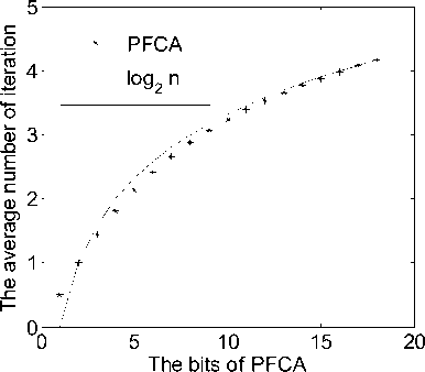
Figure 6. The average number of iteration in PFCA
The statistics data in Table1 and Fig. 6 shows: When the word length of PFCA is smaller than 18, the average number of iterations computed by the method of statistics shows that the length of carry chain of an n -bit PFCA is closed to log n .
Ш . The Implementation of PFCA in CMOS Gates
PFCA has substantial potential advantages in area and speed in theory, but there are some technological problems to resolve in the implementation of hardware circuits:
-
i ) The feedback iterations may need a synchronous clock to control the circuits, while it is n ot suitable to import system clock.
-
ii) The feedback signals must be separated from the input signals.
-
ш ) As an asynchronous circuit, PFCA requires a start and a finish signals.
-
iv ) The difference between the delays from port A and B to port S and C will be enlarged after several times of iteration, it may leads to the failure of PFCA.
-
v ) The attenuation of output signals will shorten the
transmitted distance.
This section proposed a CM OS gate implementation scheme, two rules obeyed in the design of PFCA: 1) The occupied area and time consumption should be as small as possible; 2) the delay from input A and B to output C and S should be equal. The simulation adopts the platform HSPICE2007.3 with pa rameters of MOS transistor: L =1 U , W =20 U , LEVEL =1 and other defaults.
A . The Implementation of Half Adder Trigger in CMOS Gates
A half adder trigger shown in Fig. 5 is implemented in HSPICE2007.3 and the timing sequence is shown in Fig. 7. In Fig. 7, if B = 1 , the status of S and C is oscillation waves with “0-1”; if B = 0 , C is ‘0’ all th e time no matter the transient status is ‘0’ or ‘1’ and S is determined by the transient status which is not certain, the result is
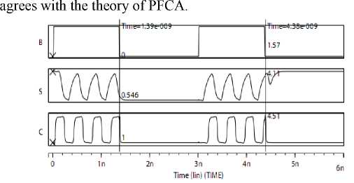
Figure 7. The time sequence of half adder trigger
-
B . The Implementation of PFCA in CMOS Gates
In the CMOS implementation scheme, at least one drive circuit should be brought in every two bit solve signal attenuation problem. A structure of 8-bit PFCA is shown in Fig. 8, and the CMOS structure of basic unit ( 2 -bit PFCA) is shown in Fig. 9.
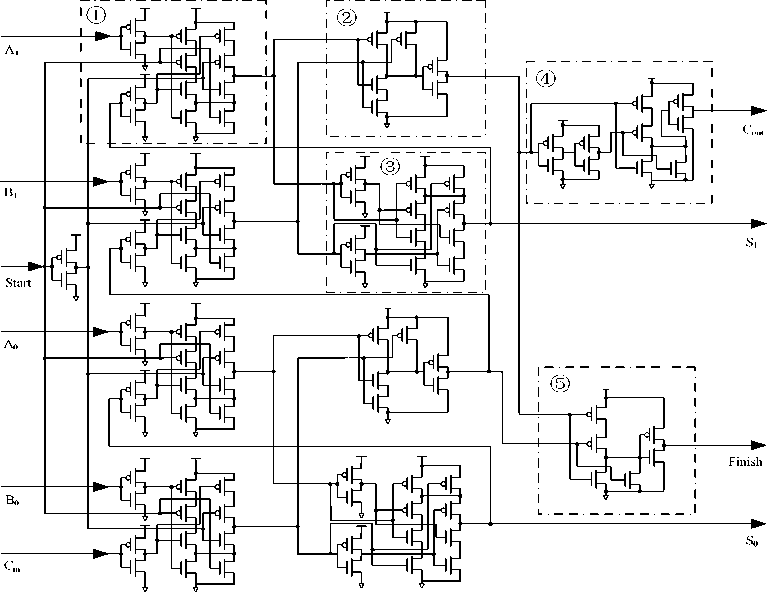
Figure 9. The CMOS structure of 2-bit PFCA
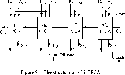
PFCA of any even bits can be cascaded by the unit shown in Fig. 9. In the Fig. 9, dashed box © encircles a MUX2-1( not include the NOT gate of Start signal); dashed box © encircles an AND gate, which generates output S ; dashed box © encircles an XOR gate, and it generates output C ; dashed box @ encircles a drive circuit of carry-output; dashed box © encircles an OR gate, which is used as a addition completion test mechanism, when OR gate output ‘0’, the addition of the 2 -bit PFCA is completed. Compared to Fig. 4, practical PFCA structure has additional two MUX2-1s, a Start, a drive circuit and a c ompletion test circuit in each unit. The controlling port Start and two MUX2-1s can resolve the problem i ) and problem i ), which gives PFCA an enable signal to select the input signals and the feedback signals. Problem ш ) is resolved by designing a mechanism to test all the output bits, If the output bits are all ‘0’, an failling edge is generated in Finish pin. Use AOI (And-Or-Inverse) gate to make up XOR gate can resolve the problem v ), as there are the same delays of 3 transistors in XOR gate and AND gate. Thus, the outputs of S and C have almost the same time computation. A drive circuit is introduced here to enhance the output signals. Simulation results show that any even length of PFCA can be implemented when the drive circuit is added in every two bits.
-
C . Timing Simulation in HSPICE
The timing simulation of 8-bit PFCA is sh own in Fig.10. To demonstrate the process of data transmitting, let A = 01111111, B = 00000001. In this case, PFCA has iterated 8 times and then got the right result, S=10000000. In Fig. 10, when the Start signal fall from ‘1’ to ‘0’, the computation begins; after 8 times iteration, the finish signal falls from ‘1’ to ‘0’, then the results come out in the outputs S0-S7. , thus PFCA finish an add operation
once. The total delay of 8 times iteration is 2.55ns and the average delay of iteration is 0.28 ns excluding the initial time 0.35 ns.
parallel carry feed back adder(8 bits)
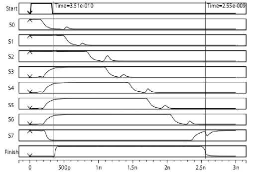
Time (lin) (TIME)
Figure 10. HSPICE simulation results of 8-bit PFCA
-
D . Eliminate Race Hazard
Race hazard is an comm on sense in Com binational logic design as is show in Fig. 10, the main reason of race hazard in Fig. 10 is the delay of input(A, B ) to C and S are not equal. If th e delay of input to C an d S Varies slightly, race hazard wouldn’t influence the final result, otherwise, circuit will be unstable. To solve this problem, more drive circuit units are in troduced in PFCA too compensate for the unequal delay of inp ut to C an d S. The improved circuit of PFCA is shown in Fig. 11 and Fig. 12.
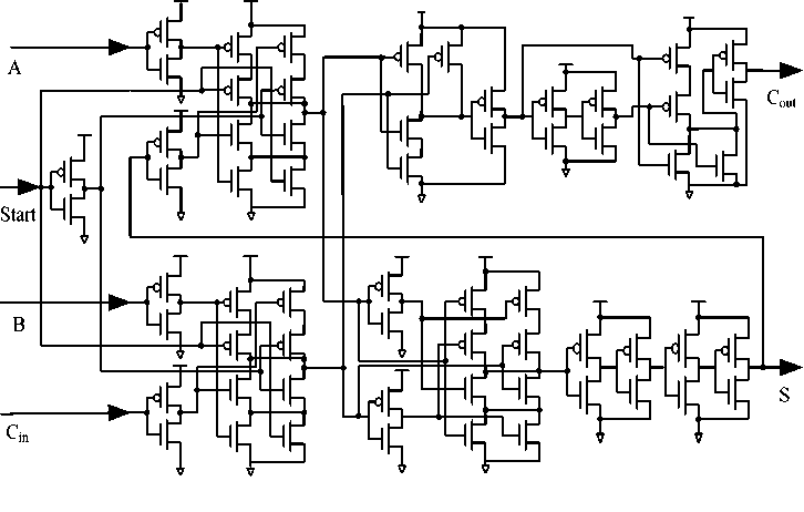
Figure 11. Improved structure of 1-bit PFCA
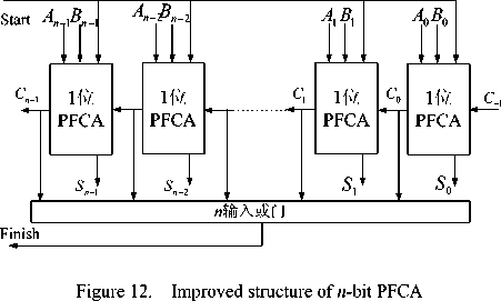
Fig. 11 is a basic unit of PFCA shown in Fig. 12.One drive circuit unit is brought in after every bit of PFCA. To compare with simulation results in Fig. 10, set let A = 01111111, B = 00000001, in this case, PFCA has iterated 8 times and then got the right result, S=10000000. The simulation results in HSPICE are sh own in Fig. 13. Obviously, race hazard has been eliminated, so the structure in Fig. 12 will be more stable.
have chosen the same CMOS gates. CLA consists of 4-bit carry look ahead unit; CSeA is created by Fixed-length grouping and each group is a 4-bit RCA.
A . The Area of PFCA
The structure of PFCA c onsists of t hree parts: half adder trigger, drive circuit and completion test unit.
One half adder trigger includes two MUX2-1, one AND gate and one XOR gate, it needs 42 transistors. Therefore n half adder triggers need 42n in total.
One drive circuit consists of two NOT gates and one OR gate and it needs 10 transistors. Given that the last two bits of PFCA don’t need drive circuit, n -bit adder needs 5n-10 transistors totally.
The completion test u nit includes several levels of n-input OR gates. One OR gate with 4 inputs needs 10 transistors. If all the OR gates adopt 4 inputs OR gate, then n -bit adder needs m = ^ log 4 n ^ levels of 4-input OR gate and each level needs the number of 4-input OR
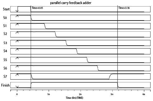
Figure 13. HSPICE simulation results of 8-bit PFCA improved structure
gate is
n
n
n
4 m
m
OR gate is
so the number of 4-input
m n
M ( n ) 1 4
in total. Thus, the
i = 1
W . Performance Evaluation of PFCA CIRCUIT
In order to evaluate the performance of P FCA, this section chose three famous adders (RCA, CLA and CSeA) to compare their area and time consumptions. Table 2 shows the simulation results of the 4 adders with different word length.
completion test u nit of n -bit adder needs 10 M ( n ) transistors .
In total, the number of transistors used in n -bit PFCA needs 47 n + 10 M ( n ) - 8 transistors including the 2 transistors used for Start signal.
Table 2 shows the number of transistors used in RCA, CLA, CSeA and PFCA when word length n=4, 8, 12, 16, 32respectively. Compared to the other three adders, the number of transistors used in PFCA is nearly as many as that in RCA, and much less than that in CLA and CSeA. What is more, the advantage will be more obvious when n is larger.
T able II.
T he results of RCA, CLA, CS e A and PFCA in the HSPICE
|
Bits |
RCA |
CLA |
CSeA |
PFCA |
||||||
|
TC |
CT |
TC |
CT |
TC |
CT |
TC |
TCT |
OCT |
ACT |
|
|
4 |
200 |
1.53 |
260 |
0.86 |
200 |
1.41 |
190 |
1.32 |
0.24 |
0.85 |
|
8 |
400 |
2.60 |
520 |
1.25 |
670 |
1.71 |
394 |
2.55 |
0.28 |
1.18 |
|
12 |
600 |
3.82 |
780 |
1.71 |
1140 |
2.02 |
594 |
3.83 |
0.29 |
1.39 |
|
16 |
800 |
4.94 |
1040 |
2.18 |
1610 |
2.32 |
794 |
5.06 |
0.29 |
1.53 |
|
32 |
1600 |
9.86 |
2080 |
3.83 |
3290 |
3.54 |
1602 |
10.08 |
0.30 |
1.87 |
TC: Transistor Count; CT: Computation Time/ns; TCT: Total Computation Time/ns;
OTC: Computation Time/ns of One iteration; ACT: Average Computation Time/ns.
The unimproved scheme (Fig. 8) is selected here for its small time consumption; it can not be the optimized scheme, so the optimized schemes [14~16] of RCA, CLA and CSeA are not adopted. Normally, we choose the standard CMOS gates, such as NOT gate, OR gate, AOI gate and OAI gate. These 4 adders (PFCA, RCA, CLA and CSeA)
B . The Time Consumption of PFCA
Let t max( n ) be the max delay of n -bit PFCA, tstart be the delay of St art signal, t 1 be the delay of once iteration and tn be the delay of average iteration. According to th e theory of n -bit PFCA and timing diagram Fig. 10:
t max( n ) = tstart + n ' t 1 , (12) The delay of avera ge iteration can be computed as follows:
tn = tstart + t 1 ' log 2 n , (13)
t start and t max( n ) can be got from Fig. 10. Then t 1 and tn can be computed by the equation (12) and equation (13). Table 2 sh ows the results, which tell us that there are som e advantages of PFCA in time consumption over other three adders and the advantages are more obvious as n increasing.
-
V. Conclusions
PFCA is a new adder based on a m ore basic logic structure and i s also feasible in hardware. Com pared to existing adders, PFCA shows obvious advantages which can be demonstrated in four parts: 1) PFCA can shorten the computation time and reduce the area consumption in a large am ount; 2) the adva ntage will be more obvious when n is larg er; 3) it is easy to im plement the PFCA even when word length n is large, because it does nothing to do with the length of adder, implementing a 1024-bit PFCA is as easily as that of a 16-bit PFCA; 4) the speed will not be influenced by the different bits PFCAs when they are used to complete the same size addition. For the operation of 8-bit addition, the computation time in 32-bit RCA is 4 times as much as in 8-bit RCA; however, they are the same when using PFCA.
The implementation scheme proposed in this paper mainly aims to verify the feasibility of PFCA in hardware implementation and it can not be the optimized scheme. If the functions of half adder trigger are made use o f sufficiently when implementing the hardware circuits, the hardware implementation of PFCA will perfo rm higher performances.
References A New Adder Theory Based on Half Adder and Implementation in CMOS Gates
- D. Goldberg, “Computer arithmetic”, Computer Architecture: A Quantitative Approach, Morgan Kaufmann Publishers, 1990.
- O.J.Bedrij, “Carry-select adder”, IRE Transactions on Electronic Computer, vol. EC-11, Jun.1962.pp.340-346.
- O. L. MacSorley, “High-speed arithmetic in binary adders”, IRE proceedings, vol.49, 1961.pp.67-91.
- S. Tuttini, “Optimal group distribution in carry-skip adders”, Proceedings of the 9th symposium on computer arithmetic, step. 1989. pp.96-103.
- A.J.Martin, “Asynchronous data paths and the design of an asynchronous adder”, Formal Method in system Design, 1(1):119-137.July.1992.
- J.D. Garside,“A CMOS VLSI Implementation of an asynchronous ALU”, Proceeding of the IFIP Working Conference on Asynchronous Design Methodologies, Manchester, England (1993).
- Cheng F C,Unger S H,Theobald M. Self-timed carry-lookahead adders[J]. IEEE Transactions on Computers, 2000,49(7):659~672.
- Cheng F C. Practical design and performance evaluation of completion detection circuits [A]. Computer Design: VLSI in computers and processors[C]. California: IEEE Computer Society, 1998.354~359.
- Singh R P P, Kumar P, Singh B. Performance analysis of fast adders using VHDL[A].International conference on advances in recent technologies in Communication and Computing[C]. California: IEEE Computer Society, 2009.189~193.
- Briley B E. Some new results on average worst case carry [J]. IEEE Transactions on Computers.1973,22(5): 459~463.
- Burks A W,Goldstine H H, Neumann J V. Preliminary discussion of the logical design of an electronic computing instrument [M]. New Jersey: Institute for Advanced Study, 1946.34~79.
- Kinniment D J.An evaluation of asynchronous addition [J].IEEE Transactions VLSI Systems.1996. 4(1): 137~140.
- Franklin M A,Pan T.Clocked and asynchronous instruction pipelines[A].Proceedings of the 26th Annual International Symposium on Micro architecture [C]. California: IEEE Computer Society Press, 1993.177 ~184.
- Vasefi F, Abid Z. 10-transistor 1-bit adders for n-bit parallel adders [A].The 16th International Conference on Microelectronics [C]. California: IEEE Computer Society Press, 2004.174 ~177.
- Vesterbacka M.A 14-transistor CMOS full adder with full voltage-swing nodes[A].IEEE Workshop on Signal Processing Systems[C].Taipei Design and Implementation.1999.713 ~ 722.
- Navia K, Foroutan V, Azghadi M R,et al. A novel low-power full-adder cell with new technique in designing logical gates based on static CMOS inverter [J].Microelectronics Journal, 2009.40: 1441~1448.
