A Novel Radiation Hardened Parallel IO Port for Highly Reliable Digital IC Design

Author: Nastaran Rajaei, Ramin Rajaei
Journal: International Journal of Modern Education and Computer Science (IJMECS) @ijmecs
Article in issue: 9 vol.8, 2016.
Free access
This article proposes a radiation hardened parallel IO port capable of tolerating radiation induced soft errors including single event upsets (SEUs) as well as single event transients (SETs). To investigate the soft error tolerance capability of the proposed design, we simulated it using the Cadence tool and showed its offered advantages. Comparing with the conventional and well-known TMR IO port, the proposed architecture results in less hardware redundancy and design cost. Through an analytical analysis, we also showed that, our design has lower failure probability than the TMR approach. It also is notable that, among the considered previous counterparts, our proposed design is the only one that is capable of tolerating both the SEUs and SETs.
Parallel IO port, Single Event Upset (SEU), Single Event Transient (SET), Triple Modular Redundancy (TMR)
Short address: https://sciup.org/15014899
IDR: 15014899
Text of the scientific article A Novel Radiation Hardened Parallel IO Port for Highly Reliable Digital IC Design
Published Online September 2016 in MECS
Following CMOS technology scaling-down and supply voltage reduction, sensitivity of CMOS circuits to radiation induced soft errors is increasing dramatically [1]. Two types of soft errors induced by radiation would occur in sequential and combinational parts of logic circuits. The phenomena of an unwanted upset of 1 to 0 or 0 to 1 in a memory cell such as an SRAM cell, level sensitive latch or flip-flop (generally sequential logic) caused by an energetic particle strike is called single event upset (SEU) [1-3]. Particle strikes could incur an unwanted glitch (a voltage pulse) in the combinational logic that is called single event transient (SET) [4-7].
To mitigate SEUs and SETs in logic circuits, triple modular redundancy (TMR) is a very conventional and widely used techniques in all levels of abstraction [8-9]. Employing three flip-flops with a voter circuit instead of one flip-flop in sequential parts can mask an SEU in one of the flip-flops and result in significant improvement in reliability of the circuit. Using the same strategy in combinational part can improve the robustness of the circuit against radiation induced SETs [10]. A schematic diagram for structure of the mentioned TMR technique in both sequential and combinational parts is shown in Fig.
-
1. The TMR approach is a very effective solution for tolerating SEUs and SETs. However, large design overhead imposed by this technique has limited its application [1].
Duplication with comparison (DwC) is another effective and also well-known technique to tolerate soft errors both in sequential and combinational logic [10]. In this technique, two copies of a module are used. A monitoring for the modules at output can be applied by an XOR gate [10]. By DwC, the occurrence of fault in one of the employed modules can be detected, but not to be located and nor to be masked [10-11]. Therefore, DwC is a fault detecting technique, while, the TMR approach is a fault detecting and also masking technique [10].
The SEU and SET soft errors can happen in different parts of a digital system such as memory units or inside of a microprocessor, such as cache memories, IO ports, combinational and sequential parts. To combat with the aforementioned soft errors, various techniques in all levels of abstraction are suggested [1-15]. One costbenefit technique for improving the robustness of digital circuits against soft errors is radiation hardening by design [1, 3, 7-10]. However, along with the more and more decrease in CMOS dimensions, the issue of single event multiple-node upset has been emerged [3, 9]. In this issue, as a result of a particle strike to today CMOS transistors, more than one node would be affected. Therefore, previous circuit level solutions for SEU/SET soft errors would not satisfy design reliability requirements [3]. For this reason, this paper focuses on module level techniques that can still satisfy needed design constraints and also reliability requirements [12].
Heretofore, some techniques for soft error tolerance of IO ports are suggested [11-15]. In the following of this paper, we will show and argue the advantages and drawbacks of the mentioned previous techniques. Also, a new module level design for IO port is proposed that basically is based on duplication. The proposed IO port is capable of masking SEUs as well as SETs with less power consumption and area overhead in comparison with the TMR technique (triplication in only flip-flops).
The next section discusses previous related work. The third section introduces our proposed radiation hardened IO port. In section 4, simulation results and analytical analyses regarding the considered designs are presented.
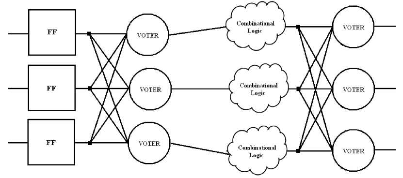
Fig.1. SEU and SET mitigation using the well-known TMR technique
-
II. Related Work
In literature, some techniques for fault tolerant design of IO ports have been proposed. In [11], the duplication technique has been used for detecting and reporting of a single bit error. In [12], a modified duplication technique was proposed that could detect an SEU or SET with a little more increase in area and power overhead compared with the traditional duplication technique. This design can improve the reliability as it is capable of detecting (and not masking) both the SEUs and SETs.
Fig. 2 shows the conventional IO port used in LEON processor [13-14] (a radiation hardened processor) or Virtex-E FPGA from Xilinx Corporation [15]. As can be found in the figure, there are two latches including one for storing the logic value that is for being written to IO pad and the other for the logic data value read from the pad. As discussed in [1-6], generally latches are prone to be affected by energetic particle strikes dramatically. Furthermore, the SETs came from combinational parts of the circuit. They could affect the data for being written into the IO pad. Therefore, SEU and SET tolerance in IO pads for reliability essential applications are necessary [12]. Fig. 3 depicts the proposed IO port in [12] and Fig. 4 shows an IO port architecture equipped with the DwC technique.
In design suggested in [12] (shown in Fig. 3), data is captured by the first latch when the write enable signal is high and is captured by the redundant latch when the write enable is low. Using this policy, an SET in input data would be detected by the XOR gate and the write error signal will be activated by the AND gate. Similarly, if an SEU happens in one of the duplicated latches, the employed XOR gate can detect the occurrence of data corruption in one of the latches. In fact, this technique can just detect the SEU/SET errors.
-
III. The Proposed Radiation Hardened IO Port
The proposed IO port shown in Fig. 5 is based on duplication redundancy. As can be seen in the figure, a voting circuitry with a feedback from the output is applied to the duplicated latches. Therefore, the next output of the voter is a majority vote of the employed two latches as well as the present state of the voter. In case of SEU occurrence in one of the duplicated latches, only one of the three inputs of the voter is faulty and hence it will result an error free output. By this strategy, a three majority voting mechanism using two latches instead of three, is implemented with occupying less area and obtaining higher reliability for SEU. Implementation of such architecture can be easily performed by the CAD tools. In the following, we will also discuss about the circuit level implementation of the proposed IO port.
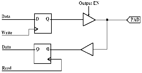
Fig.2. Conventional IO port
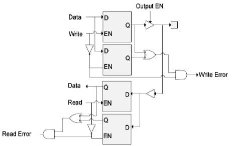
Fig.3. The proposed fault tolerant IO port in [12]
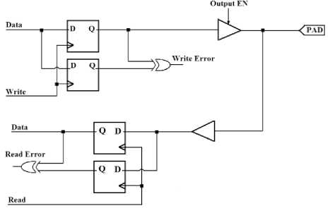
Fig.4. Duplicated IO port
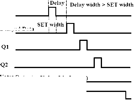
To be able to also mitigate the SETs, the input data signal (Fig. 5) is applied directly to the first latch while a delayed data signal is inputted into the second latch. Using this strategy, the SET effect will be eliminated and no consequences will be resulted by the voter. A timing diagram for data signal, the delayed data signal and output of both latches in case of SET occurrence is shown in Fig. 6. Tracking the figure, as the resulted pulses at output of the latches are not synchronic, the voter will filter out the SET pulse and a fault free output will be resulted by the voter.
The key element in our SEU/SET tolerant IO port is the voting circuitry (shown in Fig.5). In register-transfer level (RTL) design or design for field programmable gate arrays (FPGA), this architecture can be designed or described easily by the hardware description languages (HDL). Some reconsiderations in synthesis tools would be needed. In transistor level design or design for application specific integrated circuits (ASIC), a cost benefit implementation of the voter circuit is shown in Fig. 7. This circuit (the so-called guard-gate [16]) is composed of a C-element and a 4-transistor keeper. C-element is 4-transistor, 2-input and 1-output gate that acts as an inverter when the inputs are agree and takes a high impedance at its output when the inputs are disagree [1].
In this circuit, inputs I1 and I2 come from the employed two latches (Fig. 5). When an SEU occurs in one of the latches, I 1 and I 2 turn to be disagree. Therefore, keeping the previous state by the keeper, the output of the guardgate stays fault-free. When I 1 and I 2 are agree, SEU in the keeper cannot last as the C-element returns output Q to its original state. It is notable that, the suggested gaur-gate includes only eight transistors while, a transistor level implementation of the conventional voter (used in Fig.1 for the TMR technique) needs fourteen transistors [10]. Therefore, we can conclude that, our proposed IO port not only needs one latch circuit less than the TMR, but also its voter circuit is less expensive than the one of TMR.
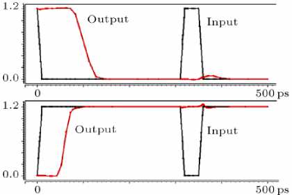
For the circuit level design, one solution for the delay element employed in our design (shown in Fig.5) can be the circuit we proposed in our earlier work [7] and shown in Fig.8. In this circuit, the amount of the delay provided by the circuit can be tuned by changing the number of transmission gates (TG) employed and also by transistor resizing. In [7], we showed that this circuit itself is capable of SET filtering. Fig.9 shows normal operation as well as the SET filtering capability of this circuit [7].
-
IV. Simulation Results
Reliability and soft error tolerance usually obtained at the expense of redundancy. In this paper, we achieved both SEU and SET tolerance capabilities using hardware redundancy. Redundancy mostly comes out by design overhead in power, delay and area [17-18]. In order to investigate the efficiency of the proposed IO port, we ran a circuit level simulation for the conventional IO port (shown in Fig. 2), the duplicated architecture (shown in Fig. 4), the new design suggested in [12], the TMR architecture and our proposed IO port (Fig. 5) using the Cadence tool with 90nm TSMC CMOS model.
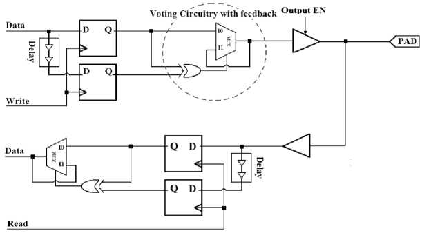
Fig.5. The Proposed radiation hardened IO port
Data
Voter Output = V(O1, Q2, Output)
Delayed Data
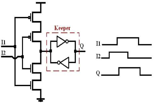
Fig.7. Circuit diagram of guard-gate and its signaling
Fig.6. Timing diagram of the proposed IO port when SET is happened
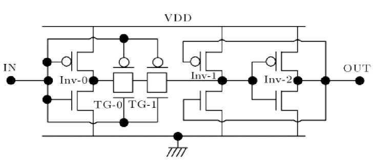
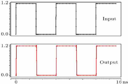
Fig.8. Proposed delay element and also SET filter in [7]
(a) (b)
Fig.9. Operation of the proposed SET filter in [7] in a) normal operation and b) in presence of SET pulse
For soft error injection, a double exponential current source proposed in [19] and employed widely [1-5] is used. The current shape of the model is given by (1).
t
Q crit = J
Q total
T f - T r
x ( e t T f
- e - t1 T r ). dt
Where Qtotal is the total induced charge, τr and τf are rise and fall time constant coefficients that the considered values for them are 1.64E-10 and 5E-11 [1, 19] respectively. This current source is applied to the considered sensitive nodes to model the induced charge by the hit energetic particle.
-
A. SEU Mitigation capability
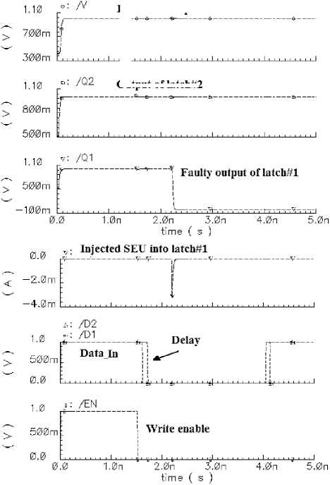
An SEU can happen in a latch when its enable signal is low and the latch is holding data sampled during the active phase [1]. In this mode (the so-called holding mode), the latch cannot capture data from input and therefore, SETs cannot affect the stored data in latch [1].
Fig. 10 shows the simulation result of an injected SEU to one of the duplicated latches (the first latch) where the write signal is low and the latches are in their holding state. As can be found from the result, although as a result of a particle strike, an SEU is happened in one of the latches, the final output of the voter is fault free.
-
B. SET Mitigation Capability
When the enable signal of a latch is high, the latch is transparent, i.e. the output of the latch is equal to its input. In this time, any SET on input data signal can affect the output of the latch [7].
To evaluate the SET mitigation capability of the proposed design, an SET is injected to input of the writelatches. The result from the associated simulation is shown in Fig. 11. As can be seen in the figure, the voter has filtered out the generated pulse and the output is fault free.
-
C. Area, Power and Performance Analysis
As expressed earlier, generally fault tolerant techniques impose redundancies in hardware, software or time resulting in power, area and performance overhead. Fault tolerant design with lower penalties in area, power and performance is the most important concern of designers in fault tolerant system design. Our proposed IO port has a fault masking capability like TMR with enhanced capability of masking the SETs, but employs the hardware redundancy as low as the duplication method. In order to evaluate power consumption and performance of our proposed design, it is compared with simple IO port, duplicated IO port, TMR IO port and the proposed method in [12]. The comparative analyses are presented in TABLE I. For an easier comparison, the quantities of power, propagation delay, power delay product (PDP) and area (in terms of transistor count) are normalized based on the associated quantities for the simple IO port. In TABLE II, a qualitative comparison in terms of SET/SEU detecting and masking capabilities among the considered designs is presented. The measured values in accomplished simulations (using the Cadence simulator with 90nm technology model) is 9µW for power consumption and 46.16ns for propagation delay of the simple IO.
The simulation results reported in TABLE I reveal that, the TMR technique has 36.1% more power consumption and 20% more area overhead than our design while it is not capable of masking the SETs. In comparison with the duplication technique, our design has 10% more power consumption and 33% more area overhead while it achieves much more reliability as it can detect and also mask both the SEU and SET soft errors. As expressed earlier, the duplication technique or the proposed designs in [11] and [12] are only capable of reporting the occurrence of an error but they cannot mask it. In other words, our proposed design has the SEU masking capability like the TMR technique (with even more reliability due to the less area overhead and fewer sensitive nodes) and also SET masking capability while occupies less area, power and delay overhead (similar to the duplication technique).
-
D. Reliability Analysis
To evaluate the SEU reliability improvement offered by our design, we compared it with the TMR technique as it is the only design with capability of SEU masking among the other techniques we considered in this paper. To do this, we consider the analytical equations proposed in [20].
Table 1. Comparison of power, delay and area overhead of the considered designs
|
IO port |
Power |
Propagation Delay |
PDP |
Area |
|
Simple |
1 |
1 |
1 |
1 |
|
Duplication |
2.16 |
1.92 |
4.148 |
2.14 |
|
Proposed in [12] |
2.32 |
1.95 |
4.52 |
2.57 |
|
TMR |
3.24 |
1.97 |
6.38 |
3.43 |
|
Our Design |
2.38 |
2.11 |
5.02 |
2.86 |
Table 2. Comparison of reliability capabilities for the considered designs
|
IO port |
SET Detection |
SEU Detection |
SET Masking |
SEU Masking |
|
Simple |
× |
× |
× |
× |
|
Duplication |
× |
V |
× |
× |
|
Proposed in [12] |
V |
V |
× |
× |
|
TMR |
× |
V |
× |
V |
|
Our Design |
V |
V |
V |
V |
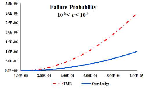
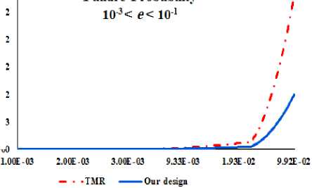
Assuming a single bit error probability of e , probability of failure in the TMR technique is given by (2). Similarly, this probability for our proposed technique is given by (3).
P TMR = 3 e 2 - 2 e 3
P j • our design
= e2
Where, P denotes the failure probability associated with the TMR technique and our design.
Fig. 12 compares the related failure probability versus the error probability e . The results confirm that, our proposed design has a considerable higher reliability (for SEU) than the conventional TMR technique. The reasoning for the obtained results is that the TMR technique employs more hardware redundancy than our proposed design. Therefore, probability of particle strikes effect in the TMR technique is more than our design [1].
Once again, it should be noted that (referring TABLE II), none of the other considered designs offer the capability of SET filtering (masking). Therefore, it does not make sense to think about the reliability improvement of our proposed design for SET errors over the other counterparts. It is notable that, based on the amount of delay provided by the employed delay element (shown in Fig. 5), SET pulses with shorter width than that delay can be filtered out by our suggested IO circuit. Obviously, larger pulses can pass the filter and emerge at the output. There should be a trade-off between the amount of the delay provided by the delay element and performance of the circuit. When our circuit is going to be employed in a high frequency application, this delay should not be so large. If we set a large delay as well as high frequency inputs, the normal changes in input would be detected as an SET pulse and the circuit would filter out the input changes. For the applications with lower frequencies, this delay can be larger to filter out larger SET pulses. Higher energetic particles would result in larger SET pulses [2022].
Generally, the SET pulses generated in combinational logics could threat functionality of the logic circuits only when they arrive to latching window of their succeeding sequential logic. In such cases, the SET pulse will be latched as a wrong data. Otherwise, the SET pulse is not a concerning soft error. In fact, when an SET pulse does not locate at a latching window, it is masked by the circuit inherently (timing masking) [2, 5]. However, by increasing the frequency of the circuits, probability of locating the SETs in latching window of the succeeding sequential logics is increasing [5].
Fault free output of voter
Output of latcb#2
Fig.10. SEU injection into latch#1 in write mode
-
V. Conclusion
3.00Е-02
In this paper, a new radiation hardened parallel IO port is proposed. This IO port can tolerate both the SEU and
SET soft errors occupying lower redundancies than the conventional TMR technique. In order to evaluate our design and prove its efficiencies, the simple IO port, DwC/TMR IO ports, the proposed IO port in [12] and our design are simulated using the Cadence simulator with 90nm technology model. Both the SEU and SET effects are injected to the proposed IO port through the performed simulations and the capabilities of our design are shown. Furthermore, an evaluation for power consumption and propagation delay are presented. As the simulation results reveal, our proposed IO port occupies redundancies as low as the DwC IO port (shown in Fig. 4) and significantly lower than TMR IO port while it can mask both the SEUs and SETs. As TABLE II discusses, only our design is capable of masking both the SEU and SET errors. We also investigated the soft error tolerance efficiency of our suggested design through an analytical analysis and showed that, how our design enjoys higher reliability than the widely used TMR technique. Some suggestions for circuit level implementation of the proposed IO port are also provided based on the previous preferable work. We can claim in conclusion that, over prior radiation hardened parallel IO ports, we not only improved the reliability, but also we decreased overhead.
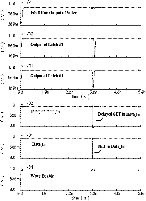
De laved Data In
Fig.11. SET injection in data_in in write mode
(a)
Fig.12. Reliability analysis of our proposed design and comparison with the TMR technique. a) 10-6< e < 10-3 and b) 10-3< e < 10-1
Failure Probability
2.50E-<12
2ЛНК-О2
1 SUE -02
1.0 HE -02
5.0OE-03
O.OOE+OO
(b)
Acknowledgements
The authors would like to acknowledge Shahid Beheshti University for support of this work.
References A Novel Radiation Hardened Parallel IO Port for Highly Reliable Digital IC Design
- R. Rajaei, M. Tabandeh, B. Rashidian, "Single Event Upset immune latch circuit design using C-Element," in Proc. of the IEEE 9th International Conference on ASIC, China, pp. 280-283, 2011.
- F. Wang and Y. Xie "An accurate and efficient model of electrical masking effect for soft errors in combinational logic," 2nd Workshop of System Effects of Logic Soft Error, Urbana-Champaign, IL, April 2006.
- R. Rajaei, B. Asgari, M. Tabandeh, M. Fazeli, "Design of Robust SRAM Cells Against Single Event Multiple Effects for Nanometer Technologies," IEEE Transactions on Device and Materials Reliability, 2015.
- W. Sootkaneung, K. K. Saluja, "Soft error reduction through gate input dependent weighted sizing in combinational circuits," in Proceedings of the 12th International Symposium on Quality Electronic Design, Santa Clara, CA, 2011.
- R. Rajaei, M. Tabandeh, M. Fazeli, "Soft Error Rate Estimation for Combinational Logic in Presence of Single Event Multiple Transients," Journal of Circuits, Systems and Computers, 2014.
- L. Artola, M. Gaillardin, G. Hubert, M. Raine, P. Paillet, "Modeling Single Event Transients in Advanced Devices and ICs," IEEE Transactions on Nuclear Science, 2015.
- R. Rajaei, M. Tabandeh, M. Fazeli, "Low Cost Circuit-Level Soft Error Mitigation Techniques for Combinational Logic," Transactions on Electrical and Computer Engineering, Scientia Iranica, Elsevier, 2015.
- B. Alidoosti, M. H. Moaiyeri, "An Energy-Efficient and Robust Voltage Level Converter for Nanoelectronics," International Journal of Modern Education and Computer Science (IJMECS), 7(5), 2015.
- R. Rajaei, B. Asgari, M. Tabandeh, M. Fazeli, "Single Event Multiple Upset-Tolerant SRAM Cell Designs for Nano-scale CMOS Technology," Turkish Journal of Electrical Engineering & Computer Sciences, 2016.
- R. Rajaei, M. Tabandeh, M. Fazeli, "Low Cost Soft Error Hardened Latch Designs for Nano-scale CMOS Technology in presence of Process Variation," Microelectronic Reliability, Elsevier, 2013.
- N. Rollins, M. J. Wirthlin1, M. Caffrey and P. Graham, "Reliability of programmable Input/Output pins in the presence of configuration upsets," Military and Aerospace Applications of Programmable Logic Devices (MAPLD), Laurel MD, USA Sep. 2002.
- M. H. Razmkhah, S. G. Miremadi, A. Ejlali, M. Fazeli, "A novel SET/SEU hardened parallel I/O port", IEEE Circuits and Systems, International Conference on Testing and Diagnosis, China, Apr 28-29, 2009,
- Gaisler research, "LEON2 processor user's manual", Version 1.0.30, datasheet, XST Edition, July 2005.
- Gaisler research, "Quad Core LEON4 SPARC V8 Processor User's Manual", datasheet, XST Edition, February 2016.
- Xilinx, "Virtex-E datasheet", 2002.
- R. L. Shuler, A. Balasubramanian, B. Narasimham, B. L. Bhuva, P. M. O. Neill, C. Kouba, "The Effectiveness of TAG or Guard-Gates in SET Suppression Using Delay and Dual-Rail Configurations at 0.35 μ m," IEEE Transactions on Nuclear Science, 2006.
- F. Sharifi, M. H. Moaiyeri, K. Navi, "A novel quaternary full adder cell based on nanotechnology," International Journal of Modern Education and Computer Science (IJMECS), 7(3), p.19. 2015.
- A. Sajid, A. Nafees, S. Rahman, "Design and Implementation of Low Power 8-bit Carry-look Ahead Adder Using Static CMOS Logic and Adiabatic Logic," International Journal of Information Technology and Computer Science (IJITCS), 2013.
- H. Cha, J. H. Patel, "A logic-level model for α-particle hits in CMOS circuits," Proc. 12th IEEE Int'l Conf. Computer Design (ICCD '93), pp. 538-542, 1993.
- R. Naseer, R. Z. Bhatti, J. Draper, "Analysis of Soft Error Mitigation Techniques for Register Files in IBM Cu-08 90nm Technology," Circuits and Systems, 2006. MWSCAS '06. 49th IEEE International Midwest Symposium on, vol.1, no., pp.515-519, 6-9 Aug. 2006.
- R. Rajaei, M. Tabandeh, M. Fazeli, "Single Event Multiple Upset (SEMU) Tolerant Latch Designs in Presence of Process and Temperature Variations," Journal of Circuits, Systems and Computers, 2015.
- M. Kaviani, H. Sharifi, M. Dolatshahi, K. Navi, "Design of Low Voltage and High-Speed BiCMOS Buffer for Driving Large Load Capacitor," International Journal of Engineering and Manufacturing (IJEM), 2016.
