A Two Layers Novel Low-Cost and Optimized Embedded Board Based on TMS320C6713 DSP and Spartan-3 FPGA

Author: Bahram Rashidi, Ghader Karimian
Journal: International Journal of Modern Education and Computer Science (IJMECS) @ijmecs
Article in issue: 4 vol.5, 2013.
Free access
This paper presents the design and implementation of a new low-cost and minimum embedded board based on TMS320C6713 (PYP 208-PIN (PQFP)) DSP and Spartan-3 (XCS400-4PQG208C) FPGA in two layers with mount elements on two sides of the board. The proposed embedded board was developed satisfactorily for different applications such as data acquisition of sensor’s with serial port, control units, finite state machines, signal processing algorithms, navigation computing, Kalman filtering etc. Goal of the design was to implement as many as possible low-cost and minimum sizes of the board, also to receive input signals in a short time period and as real time. The board features are include: mount elements in two side of the board for minimization of the proposed board and also placed decoupling capacitors (by pass) for the DSP and FPGA in bottom layer of board strictly below these two ICs because should be placed as close as possible to the power supply pins DSP and FPGA, GND polygon layer is used in total top layer and microcomputer ground for DSP & FPGA in bottom layer, use FPGA for two aim ones for implementation of glue logic total of board and interface between serial connectors, use three RS-232 serial port, one RS-422, and SPI serial port on FPGA, use MT48LC16M16A SDRAM-256MB(4*4MB*16), Am29LV400B Flash memory 4 Megabit (512 K x 8-Bit/256 K x 16-Bit) and XCF02S configuration PROM. The size of the proposed embedded board is 11.1cm*17. 7cm so this board is optimized of aspect cost, performance, power, weight, and size.
Embedded system design, embedded processors, reconfigurable architectures, Low-Cost, Digital Algorithms, microcomputer ground, data acquisition, real time
Short address: https://sciup.org/15014542
IDR: 15014542
Text of the scientific article A Two Layers Novel Low-Cost and Optimized Embedded Board Based on TMS320C6713 DSP and Spartan-3 FPGA
Published Online May 2013 in MECS and Computer Science
-
[1] Introduction
An embedded system is one with a built-in or embedded processor or computer, typically for carrying out some kind of real-time applications and should have some kind of connection to the outside world. It is the application rather than the hardware itself that defines the embedded system. Embedded Systems have been around since the early days of computers. However, in those days, the number of such systems was not very large basically because of the hardware cost. Although there are infinite varieties of embedded systems, the principles of operation, system components and design methodologies are essentially the same but vary in complexity depending on the application. Embedded systems are used typically to carry out real-time applications. A real-time embedded system can be viewed as an embedded system in which the time at which the output (result) produced is significant and critical. The lag from input time to output time must be sufficiently small for acceptable timelines. Alternatively, real-time embedded system receives inputs and sends outputs to the target system at times determined by the target system operational consideration’s supported by a real time program for the correctness of operation depending on the logical results of the computation and the time at which the results are produced. Based on time constraints, real time systems can be hard real-time which must satisfy deadlines on each and every occasion. The real-time program is conscious of time by means of a system clock and actions are taken at the precise moments of time. Real-time system can also be a soft real-time system with occasional failure to meet deadlines acceptable where an event-based system does not have the sense of time. Early embedded systems were supervisory control systems that used steady-state optimization calculation’s to determine the set points for standard analogue controllers but they have been replaced with direct digital control, which allows the direct real-time system control. Furthermore, real-time programs manageable for small systems with well-defined tasks have also been replaced by combining supervisory control with direct digital control unit, but with increased programming complexity. This has led to the development of general-purpose real-time operating systems (RTOSs) and high-level languages for such systems with enhanced flexibility for assembly language programming of the embedded processor. Embedded systems are within every industry, from aerospace to consumer applications. With the new advances in embedded systems design, more complex applications may be implemented. During the development of an embedded system certain process models are followed. These models usually include the development of a working prototype of the final system. Embedded systems are single-functioned systems which are tightly constrained by power and cost, and are reactive and realtime [1]. In this paper, we design and implement a new low-cost and minimum embedded board in two layers based on TMS320C6713 DSP and Spartan-3 FPGA. The proposed board is for implementation of computation mathematical, process digital algorithms and serial data acquisition. We for select total of elements using optimized elements and with minimum footprint. The total of the elements is SMD until we have better and better electrical characteristics and also have smaller sizes. In this board DSP and FPGA are reprogramming to JTAG emulator. For configuration and boot process of DSP we use the secondary boot loader that assembly program boot and other files are burned by flash burn utility on flash memory. Thus for DSP programming us using one header 7*2 (P4) for JTAG emulator (XDS510), another header (P_8) for select between emulation operation (normal DSP operation) and boundary scan operation, and also for FPGA programming in the proposed embedded board we use a XCF02S serial configuration Flash PROM to store FPGA configuration data and potentially additional non-volatile data, including Micro-Blaze application code. To configure the FPGA from Platform Flash memory P5 header is used. The remainder of the paper is organized as follows: section II focuses on related works, section III emphasizes on the proposed hardware for the embedded board, description of the power supply is presented in section IV, the proposed PCB design of the embedded board is in the section V and in section VI comparison and experimentation is presented and also final section VII provides the conclusion of this paper.
-
[2] RELATED WORK
In recent years, a number of companies have been proposed for Implementation of embedded board by using the FPGA and DSP has been produced by some companies [2-10]. In following we present some companies, among many of the companies the Micromodules designed by Trenz Electronic feature modern Xilinx FPGA's. With small size and high-density connectors, they can be used nearly everywhere. Integrated USB2.0 guarantees high data transfer rates to a host PC. Trenz Electronic TE0630 series [2] are industrial-grade FPGA micro-modules integrating a leading-edge Xilinx Spartan-6 FPGA, a mini-USB 2.0 device port, 1 Gbit (128-Mbyte) DDR3 SDRAM with 16-bit width, 8 Mbyte Flash memory for configuration and operation, and power switch-mode power supplies for all on-board voltages. A large number of configurable I/Os are provided via rugged high-speed stacking connectors. TE0630 is fully mechanical and largely electrically backward compatible with Trenz Electronic TE0300 Xilinx Spartan-3E FPGA micro-
modules. All this on a tiny footprint, smaller than a credit card, at the most competitive price. Hardware and software development environment as well as reference designs are available free of charge. Also Trenz Electronic GigaBee XC6SLX series [3], are industrialgrade FPGA micromodules integrating a leading-edge Xilinx Spartan-6 LX FPGA, Gigabit Ethernet transceiver (physical layer), two independent banks of 16-bit-wide 128 MByte DDR3 SDRAM, 8 Mbyte SPI Flash memory for configuration and operation, and power switch-mode power supplies for all on-board voltages. A large number of configurable I/Os is provided via robust board-to-board (B2B) connectors. TE0320 (Spartan-3A DSP) Industrial Micromodule Series [4], are is an industrial-grade FPGA micromodule integrating a leading-edge Xilinx Spartan-3A DSP FPGA, a USB 2.0 microcontroller, 32-bit wide 128 MByte DDR RAM, 4 MByte Flash memory for configuration and operation, and power switch mode power supplies for all on-board voltages. Board TI DSP TMS320C6713 200M and Altera FPGA Cyclone II EP2C5 [5], is a very high performance for audio and video operation by cooperating DSP and FPGA. In [6], a DSP6713 high speed data acquisition board is presented, OURS-DSP6713, which uses high speed float point TMS320C6713PYP200 DSP to real-time collect and process multi-channel data, is an ideal platform for high speed data acquisition system. The data are transferred to the PC terminal interface for real-time waveform display and storage via USB2.0 interface. Specification of the [6] includes educational instrument, industrial control, environment monitor, data acquisition. In [7], a high speed digital signal processing board (DSPCARD) based on Analog Devices Blackfin 532 DSP and a Xilinx Spartan III FPGA are presented. In [8], presented six embedded boards two of the boards are based on floating point DSP processor include; C6713Compact TMS320C6713 DSP Board with Virtex-II FPGA and C6713CPU TMS320C6713 Embedded DSP Board with Spartan-3 FPGA. Four of the boards are based on a fixed point (integer) DSP processor include; TMS320C6412 DSP Board with Spartan-3 FPGA and USB 2.0, C6418CPU TMS320C6418 Embedded DSP Board with Spartan-3E FPGA, C6413CPU TMS320C641x Embedded DSP Board with Spartan-3E FPGA, and C6410CPU TMS320C641x Embedded DSP Board with Spartan-3E FPGA. The Spartan-3A Starter Platform [9] provides a platform for engineers designing with the Xilinx Spartan-3A DSP FPGA. The board provides the hardware to not only evaluate the advanced features of the Spartan-3A DSP, but also to implement complete user applications using peripherals on the Spartan-3A DSP Starter Platform and EXP modules, or both, plugged into EXP expansion connectors on the Spartan-3A DSP Starter Platform. In section VII detail of comparison different characters of the proposed work and related work is presented. Also in [10], The Cyclone II DSP development board is included in the DSP Development Kit, Cyclone II Edition. The Cyclone II DSP development board provides a low-cost hardware
platform for developing high performance DSP designs based on Altera Cyclone II FPGA devices. The DSP Development Kit, Cyclone II Edition features the EP2C70F672 FPGA. This work is designed in more than two layers. And the size of their work is more than the size of the proposed board.
-
[3] DESCRIPTION OF THE HARDWARE OF PROPOSED EMBEDDED BOARD
DSP and FPGA are complementary solutions that provide best-of-both-world processing approaches for high performance real time signal processing systems, and allow designers to capitalize on two complementary technologies where they are best suited. Programmable DSPs are the classic answer to real time signal processing. They offer high-speed, real-time processing performance, low unit power consumption and affordable unit prices. Software programmability also makes them very flexible. FPGAs are increasingly used in real time signal processing. They offer very high performance (parallel processing), flexibility through programmable hardware and affordable cost of complementary functions. Complementary Solution FPGAs typically complement programmable DSPs in high-performance real-time systems in one or more of the following ways:
-
1. Performance acceleration in the signal processing
-
2. System logic maxing and consolidation
-
3. New peripheral or bus interface implementation
-
4.
DSP and FPGA are two different methods used for signal processing. Both technologies are good depending on the processing requirement. For example, there are many high sampling rate applications that an FPGA does easily, while the DSP, generally speaking, is more oriented toward lower sampling rates. On the other hand, many complex software problems cannot be addressed by an FPGA [11]. With the development of DSP and FPGA technology in the recent years, these are more and more applications using of combined DSP and FPGA applied widely in digital signal processing. Although embedded systems are application specific, some degree of re-programmability is desired and essential. The reprogrammability assists when upgrading the devices, it is much easier to change the software slightly rather than develop the entire hardware from scratch. In this work, the FPGA is used for creating an efficient interface of the sensor with serial data and other peripherals with the DSP, Therefore, three RS-232 ports, one RS-422 port and, one SPI port are created and connected to the FPGA. So it tends to reduce the number of chips in a compact system.
-
A. Proposed Hardware for The DSP Processor
The TMS320C67x DSPs compose the floating-point DSP generation in the TMS320C6000 DSP platform. The C6713 device is based on the high-performance, advanced very-long-instruction-word (VLIW)
architecture developed by Texas Instruments (TI), making this DSP an excellent choice for multichannel and multifunction applications. Operating at 200 MHz, the C6713 delivers up to 1350 million floating-point operations per second (MFLOPS), 1800 million instructions per second (MIPS), and with dual fixed-/floating-point multipliers up to 450 million multiply-accumulate operations per second (MMACS). The C6713 uses a two-level cache-based architecture and has a powerful and diverse set of peripherals. The Level 1 program cache (L1P) is a 4K-byte direct-mapped cache and the Level 1 data cache (L1D) is a 4K-byte 2-way set-associative cache. The Level 2 memory/cache (L2) consists of a 256K-byte memory space that is shared between program and data space. 64K bytes of the 256K bytes in L2 memory can be configured as mapped memory, cache, or combinations of the two. The remaining 192K bytes in L2 serve as mapped SRAM. The C6713 has a rich peripheral set that includes two Multichannel Audio Serial Ports (McASPs), two Multichannel Buffered Serial Ports (McBSPs), two Inter-Integrated Circuit (I2C) buses, one dedicated General-Purpose Input/Output (GPIO) module, two general-purpose timers, a host-port interface (HPI), and a glue less external memory interface (EMIF) capable of interfacing to SDRAM, SBSRAM, and asynchronous peripherals. The two I2C ports on the TMS320C6713 allow the DSP to easily control peripheral devices and communicate with a host processor. In addition, the standard multichannel buffered serial port (McBSP) may be used to communicate with serial peripheral interface (SPI) mode peripheral devices [12]. The TMS320C6713 device has two boot modes: from the HPI or from external asynchronous ROM.
In this proposed embedded board, we use two memories for connecting to DSP and FPGA. These two memories include one SDRAM (MT48LC16M16A (256MB(4*4MB*16))), for storage of data and one flash memory, Am29LV400B4 Megabit (512K x 8-Bit/256K x 16-Bit) for boot processing of the DSP (secondary boot loader and application program are burnt on flash detail this part is proposed in section 3). Data bus between the DSP, SDRAM, and flash memory are 16-bit. In the proposed design DSP processor is connected to SDRAM, Flash memory, and FPGA. Common signals between these four elements are addressed line (A2-A21) and data line (D0-D15). In the below we describe the interface between the DSP and SDRAM also in following explanation of the interface between the DSP and flash memory are proposed.
-
a. SDRAM Interface
SDRAM is commonly used in applications that require a large amount of memory at faster speeds thus offer the densest and most economical solution for large memory arrays, For example image processing. The disadvantage of SDRAM is the number of control cycles required for operation. The 256Mb SDRAM is a highspeed CMOS, dynamic random-access memory containing 268,435,456 bits. It is internally configured as a quad- bank DRAM with a synchronous interface (all signals are registered on the positive edge of the clock signal, CLK). The external memory interfaces (EMIFs) of all C6000 devices support a glue less interface to a variety of external devices, including: Pipelined synchronous-burst SRAM (SBSRAM), Synchronous DRAM (SDRAM), Asynchronous devices, including SRAM, ROM, and FIFOs, An external shared-memory device. The C6000 EMIF has a one cycle command-to-command turnaround time. At least 1 data dead cycle is always included between commands so that read data and write data are never driven in the same cycle.
The C621x/C671x EMIF service requests of the external bus from two requests: 1- On-chip enhanced direct-memory access (EDMA) controller. 2- External shared-memory device controller. The C621x/C671x EMIF has the following features: All of the memories interfacing with the C621x/C671x EMIF should operate off of ECLKOUT (EMIF clock output). On the C6713 DSP, ECLKOUT runs at either ECLKIN or SYSCLK3, configurable using the EKSRC bit in DEVCFG. SYSCLK3 is an internally-generated divide-down clock with programmable divide ratio and the PLL output as the reference clock. All other C621x/C671x devices require that the system provides an external clock source (ECLKIN). The ECLKOUT signal is produced internally based on ECLKIN or SYSCLK3 (C6713 DSP only). If desired, the CLKOUT2 output can be routed back to the ECLKIN input. The SDRAM, SBSRAM, and asynchronous signals are combined. A system can include all three memory types, since no background refresh is performed. Unlike the C620x/C670x EMIF, the C621x/C671x EMIF space CE1 supports all three types of memory. The synchronized memory interfaces use a four-word burst length that is optimized for the two-level cache architecture. The SDRAM interface is flexible, allowing interfaces to a wide range of SDRAM configurations. The SDA10 pin has been removed. Address pin EA (12) serves the function of the SDA10 pin for the SDRAM memories. The C621x/C671x EMIF supports memory widths of 8 bits, 16 bits, and 32 bits, including reads and writes of both big- and little-endian devices. The C6712 EMIF supports memory widths of 8 bits and 16 bits only. There is no distinction between ROM and asynchronous interface. For all memory types, the address is internally shifted to compensate for memory widths of less than 32 bits. The least-significant address bit is always output on external address pin EA2, regardless of the width of the device. Accesses to 8-bit memories have logical address bit 0 output on EA2. The EMIF automatically performs packing and unpacking for word accesses to external memories of less than 32 bits. For a 32-bit write to an 8-bit memory, The EMIF automatically unpacks the data into bytes such that the bytes are written to byte address N, N + 1, N + 2, then N + 3. Likewise, for 32-bit read from a 16-bit memory, the EMIF takes the data from half word address N, then N + 1, packed into a 32-bit word, then written to its destination. The byte lane used depends on the endianness of the system. The C621x/C671x EMIF allows programming of the addressing characteristics of the SDRAM, including the number of column address bits (page size), row address bits (pages per bank), and banks (maximum number of pages that can be opened). The C621x/C671x EMIF can interface to any SDRAM that has 8 to 10 column address pins, 11 to 13 row address pins, and two or four banks. Other SDRAM configurations are also possible, as long as they are subsets of the column, row, and bank bits supported by the C621x/C671x DSP. The number of EMIF address registers limits the maximum number of open pages. Using this information, the C621x/C671x EMIF may open up to four pages of SDRAM simultaneously. The pages can all be in different banks of a single CE space or distributed across multiple CE spaces. Only one page can be open per bank at a time.
Now based on above description SDRAM connected to the DSP. Fig. 1 shows the configuration between SDRAM and DSP in the proposed design.
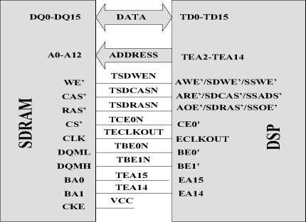
Fig.1: Configuration between SDRAM and DSP in proposed design
-
b. Flash Memory Interface
The asynchronous interface offers users configurable memory cycle types used to interface to a variety of memory and peripheral types, including SRAM, EPROM, and flash, as well as FPGA and ASIC designs. However, this section focuses on the interface between the EMIF and flash memory, which is very similar to a ROM or EEPROM interface. Flash memory is commonly available on the market in either 8-bit-wide devices or configurable 8-/16-bit-wide devices. The configurable devices generally have 16 data I/O lines, but a mode select pin tells the device whether to operate in8- or 16-bit mode. If more depth is required than can be provided via an 8- or 16-bit-wide flash memory device, then these devices can be used in parallel to create a x32/x64 bit interface. Due to the asynchronous interface, some logic will be needed between the RY/BY and the EMIF ARDY signal to verify that all the flash devices are ready. If glue is not used in the interface, then all the D (x) bits from the flash will need to be polled to verify that all the 8-or 16-bit ROMs are ready. In 8-bit mode, D (15) operates as the least significant bit of the address, thus giving a 2n+2-byte address space.
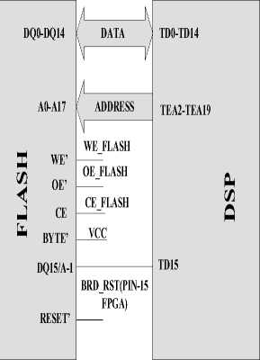
Notice that the diagram shows no common clock interface between the C6000 and Flash, as indicated by the term asynchronous. The EMIF still uses the internal clock to coordinate the timing of its signals, however, the flash responds to the signals at its inputs regardless of any clock. Fig. 2 shows the configuration between FLASH and DSP in the proposed design.
FLSHCEN(FPGA)
CE_FLASH
CE1' 3
FLASHOEN(FPGA)
OE_FLASH 2
AOE’/SDRAS’/SSOE’
FLASHWEN(FPGA)
WE_FLASH _2
AWE’/SDWE’/SSWE’
Fig. 2: Configuration between Flash memory and DSP in proposed design.
|
PIN_181 - PIN_204 PIN_34 - PIN_3 PIN_16 PIN_19 PIN_22 < PIN_36 о PIN_67 Р- PIN_20 PIN_169 PIN_172 PIN_181 PIN_162 PIN_64 - PIN_61 PIN_58 PIN_166 |
DATA \ / /------\ ADDRESS TSDWEN TSDCASN TSDRASN TCE3N NMI TECLKOUT HD14 HD12 HD8 HD4 EINT4_EINT7 TOUT1 DSP_RST |
TD0-TD15 TEA2-TEA21 AWE’/SDWE’/SSWE’ ARE’/SDCAS’/SSADS’ AOE’/SDRAS’/SSOE’ CE3' NMI ECLKOUT HD14/GP(14) HD12/GP(12) HD8/GP(8) HD4/GP(4) EXT_INT4-EXT_INT7 TOUT1 RESET’ |
-
B. Proposed Hardware for The FPGA
In this design FPGA play three roles, first role is a data acquisition of serial ports and other peripheral interface (P3 and P2 header (2*10)). The proposed board provides two expansion connectors for easy interface flexibility to other off-board components. P3 header is connected to BANK2 of FPGA and also P2 header is connected to BANK3 and BANK4 of the FPGA. As shown in Fig. 4, the proposed embedded board has three RS-232 serial Ports with male DTE connector based on ICs MAX3232. BANK3 of FPGA moreover relate to P2 header also related with received signals and transmitted signals of three RS-232 and RS-422. The DCE-style port connects directly to the serial port connector available on most personal computers and workstations via a standard straight-through serial cable. Null modem, gender changers, or crossover cables are not required. Use the DTE-style connector to control other RS-232 peripherals, such as modems or printers, or perform simple loopback testing with the DCE connector. Note that Fig. 4 shows the view looking “out” the DTE connector. Fig. 4 shows the connection between the FPGA and the DB9 connectors in the proposed implementation. The FPGA supplies serial output data using LVTTL or LVCMOS levels to the Maxim device, which in turn, converts the logic value of the appropriate RS-232 voltage level. Likewise, the Maxim device converts the RS-232 serial input data to LVTTL levels for the FPGA. A series resistor between the Maxim output pin and the FPGA’s RXD pin protects against accidental logic conflicts. Hardware flow control is not supported on the connector. The port’s DCD, DTR, and DSR signals connect together, as shown in Fig. 4. Similarly, the port’s RTS and CTS signals connect together. In this configuration we using ICs MAX 3232 because of IC MAX3232 contains two IC MAX232. Thus instead use two MAX232 we only using one Max3232, Until the size of board reduced.
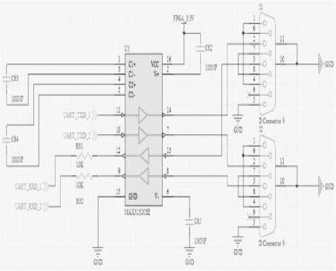
Fig. 4: Configuration between RS-232 and FPGA based on IC MAX3232
Now for RS-422 serial port we used ICs 3.3V, Low Power, High Speed or Slew Rate Limited, RS-485/RS-422 Transceivers called ISL83485 until the RS-422 protocol convert to RS-232. As explained in [13], These Intersil RS-485/RS-422 devices are BiCMOS 3.3V powered, single transceivers that meet both the RS-485 and RS-422 standards for balanced communication. Unlike competitive devices, this Intersil family is specified for 10% tolerance supplies (3V to 3.6V). The ISL83483 and ISL83488 utilize slew rate limited drivers which reduce EMI, and minimize reflections from improperly terminated transmission lines, or unterminated stubs in multi drop and multipoint applications. Data rates up to 10Mbps are achievable by using the ISL83485, ISL83490, or ISL83491, which feature higher slew rates. Logic inputs (e.g., DI and DE) accept signals in excess of 5.5V, making them compatible with 5V logic families. Receiver (Rx) inputs feature a “fail-safe if open” design, which ensures a logic high output if Rx inputs are floating. All devices present a “single unit load” to the RS-485 bus, which allows up to 32 transceivers on the network. Driver (TX) outputs are short circuit protected, even for voltages exceeding the power supply voltage. Additionally, on-chip thermal shutdown circuitry disables the TX outputs to prevent damage if power dissipation becomes excessive.
The second role of the FPGA, read and write data on DSP and SDRAM. Third role, in addition these two roles we implement a total of board glue logic on the FPGA that ties the board components together. In current embedded boards this role implements on one CPLD for example in board TMS320C6713. So we for reduce number of elements implement glue logic on FPGA instead CPLD. The FPGA register allows users to control FPGA functions in software. On the proposed low-cost embedded board the register is primarily used to access the LEDs and DIP switches. It appears as 8-bit register with a simple asynchronous memory interface. USER_REG Register is used to read the state of the 4 DIP switches and turn the 4 LEDs on or off to allow the user to interact with the embedded board. The DIP switches are read by reading the top 4 bits of the register and the LEDs are set by writing to the low 4 bits, also by this glue logic we can reset elements include Flash memory and DSP by S1 button. VHDL code of glue logic related with new low-cost embedded board given in appendix A of the paper. The FPGA implements simple random logic functions that eliminate the need for additional discrete devices. In particular, the FPGA aggregates the various reset signals coming from the reset button and power supervisors and generates a global reset. Thus instead of use CPLD we implemented glue logic on FPGA. In proposed board FPGA done above three roles, so we reduced extra hardware and only using one FPGA.
-
a. Configuration of FPGA and Reading User Data from Configuration PROMs
This interface allows the FPGA to retrieve data from the PROM before and after configuration and is the simplest implementation for reading user-defined data from a configuration PROM [14]. As explained in [15], After an FPGA is configured, it is often necessary to retrieve user-defined data that are used by the FPGA during operation. The user-defined data needs to be retrieved from an external storage device, requiring an external control circuit to interface with the storage device. This requirement implies additional time for logic design and board level engineering, not to mention extra board real estate requirements and a higher FPGA pin count. Xilinx configuration PROMs are generally used to store an FPGA design, which is downloaded to the FPGA upon system power-up. In most cases, configuration storage is the PROM’s only function, and its capacity is usually not fully used by the FPGA design, leaving the unused portion of the PROM as wasted space. Spartan-3 FPGAs are programmed by loading configuration data into robust, reprogrammable, static CMOS Configuration Latches (CCLs) that collectively control all functional elements and routing resources. Before powering on the FPGA, configuration data is stored externally in a prom or some other non-volatile medium either on or off the board, after applying power, the configuration data is written to the FPGA using any of five different modes: master parallel, slave parallels, master serial, slave serial, and boundary scan (JTAG). The master and slave parallel modes use an 8-bit-wide select map port. Depending on the system design, several configuration modes are supported, selectable via mode pins. The mode pins M0, M1, and M2 are dedicated pins.
-
b. Configuration Modes
Spartan-3 supports the following five configuration modes:
-
• Slave Serial mode
-
• Master Serial mode
-
• Slave Parallel (Select MAP) mode
-
• Master Parallel (Select MAP) mode
-
• Boundary-Scan (JTAG) mode (IEEE 1532/IEEE
1149.1)
In this design we only use two modes; Master serial mode and Boundary-Scan (JTAG) mode (IEEE 1532/IEEE 1149.1) .
-
■ Master Serial Mode:
In Master Serial mode, as explained in [15], the FPGA drives CCLK pin, which behaves as a bidirectional I/O pin. The master FPGA drives the configuration clock on the CCLK pin to the Xilinx Serial PROM, which, in response, provides bit-serial data to the FPGA’s DIN input. The FPGA accepts this data on each rising CCLK edge. After the master FPGA finishes configuring, it passes the data on its DOUT pin to the next FPGA device in a daisy-chain. The DOUT data appear after the falling CCLK clock edge. The Master Serial mode interface is identical to Slave Serial except that an internal oscillator generates the configuration clock (CCLK). A wide range of frequencies can be selected for CCLK, which always starts at a default frequency of 6MHz. Configuration bits then switch CCLK to a higher frequency for the remainder of the configuration.
-
■ Boundary-Scan (JTAG) Mode:
In Boundary-Scan mode, dedicated pins are used for configuring the FPGA. The configuration is done entirely through the IEEE 1149.1 Test Access Port (TAP). FPGA configuration using the Boundary-Scan mode is compatible with the IEEE Std 1149.1-1993 standard and IEEE Std 1532 for In-System Configurable (ISC) devices. Configuration through the boundary-scan port is always available, regardless of the selected configuration mode. In some cases, however, the mode pin setting may affect proper programming of the device due to various interactions. For example, if the mode pins are set to Master Serial or Master Parallel mode, and the associated PROM is already programmed with a valid configuration image, then there is potential for configuration interference between the JTAG and PROM data. Selecting the Boundary-Scan mode disables the other modes and is the most reliable mode when programming via JTAG [15]. We use P6 header to select between two mode Master Serial and JTAG mode with one jumper between 2 and 3 pins or 2 and 1 pin. Proposed configuration JTAG connector for relate to computer and FPGA programming is implemented based on P5 header.
-
c. Configuration Boot Process and JTAG Connector for the Dsp
In many DSP applications there is a need to copy code and/or data from one location to another at boot. C6000 DSPs offer three types of boot configurations: no boot process, ROM boot process, and host boot process. The most commonly selected boot configuration is the ROM boot process. When ROM boot is selected as the boot configuration, 1k byte (on C621X/C671X/C64X) of code will automatically be copied from CE1 to address 0 by the EDMA following the release of RESET while the CPU is stalled. DSP applications are not limited to 1k
byte of code. In the event the application size exceeds 1k byte, the accustom boot routine will need to be developed to copy the additional sections of code not copied by the ROM boot, or the secondary boot loader. In the applications that require a secondary boot loader, this custom boot code usually resides at the beginning of ROM memory so that it can be automatically transferred by the on-chip boot loader to internal memory, address 0. Ones the transfer is complete, the CPU begins executing from address 0 and therefore runs the custom boot code. The secondary boot loader then copies the rest of the application into application is boot loader using a secondary boot loader Refer to the Creating a Second-Level Bootloader for FLASH Bootloading on TMS320C6000 Platform With Code Composer Studio (SPRA999A1) for more details on Secondary Bootloader. Designing a TMS320C6000 DSP board to utilize all of the functionality of the JTAG scan path is a simple process, but a few considerations must be taken into account. The default state of the emulation signals determines whether the JTAG port is used for emulation or for boundary scan. It is therefore necessary to provide flexibility in the design to accommodate those modes that are desired. Through proper design, the JTAG interface can be used to facilitate emulation and/or boundary scan. The IEEE 1149.1 specification covers the requirements for the test access port (TAP) bus slave devices. A superset of this specification is applied to the bus master (emulator) devices. The TMS320C6000 generation of DSPs uses the JTAG scan path for boundary scan and/or emulation. There are several layout considerations that must be taken into account when designing a board for emulation and/or boundary scan [16].
-
■ Emulation and Boundary Scan Modes
The emulation signals, EMUn, exist for emulation capability of the DSP. Two of these emulation signals, EMU0 and EMU1, also select between emulation operation (normal DSP operation) and boundary scan operation. The selection is made through pull-up and pull-down resistors. It is therefore critical that the DSP board layout corresponds to the desired JTAG function(s). TRST holds the boundary scan logic in reset (normal DSP operation) when pulled low (its default state, since TRST on all C6000 devices has an internal pull-down resistor). On C620x/C670x, EMU0 and EMU1 do not feature internal pull-up resistors; therefore, external resistors must be provided. On C621x/C671x and TMS320C64x, the internal pull-up ensures that at power up, the C6000 DSP functions in its normal (non-test) operation mode if TRST is not connected. Otherwise, TRST should be driven by the boundary scan controller. Boundary scan test cannot be performed while the TRST pin is pulled low. Once TCK is clocking, the JTAG port of C6000 DSP latches EMU0 and EMU1 on the rising edge of TRST, to select between emulation operation and boundary scan modes. On C621x/C671x and C64x, the EMU0 and EMU1 pins are internally pulled up with a dedicated 30kΩ resistor;
therefore, for emulation and normal operation, no external pull-up/pull-down resistors are necessary. For boundary scan operation, pull down the EMU0 and EMU1 with a dedicated 1kΩ resistor on C621x/C671x and C64x. On the C620x/C670x, pull up EMU0 and EMU1 with a dedicated 20kΩ resistor for emulation and normal operation, and pull down EMU0 and EMU1 with a dedicated 20kΩ for boundary scan. There are two test access ports (TAPs), one for boundary scan and one for emulation. When EMU0 and EMU1 are pulled high, both TAPs are included in the scan path, and only emulation is possible. When EMU0 and EMU1 are pulled low, then only the boundary scan TAP is in the path, and the only boundary scan is possible. Often it is desirable to enable the use of both emulation and boundary scan on the DSP board. This is true if a boundary scan test software is used to verify the connectivity and functionality of JTAG devices on the board, or if in-system programmable (ISP) devices are used [16]. In this proposed embedded board we use the circuit shown in Fig. 5 for JTAG connection.
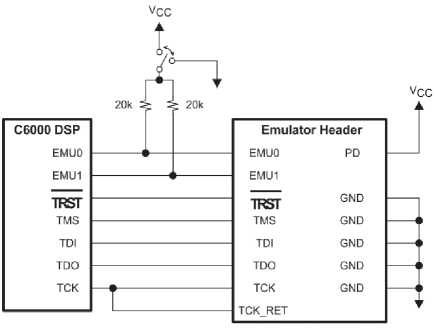
Fig. 5: JTAG Connection used in the proposed design
-
■ Configuration Switches Enable Debugging in Different Modes
TMS320C6000 DSPs are configurable to run in different modes. Although a system only requires a specific setup for its application, it is beneficial to provide a means to operate in different modes during debug. This may be accomplished by providing switches (or jumpers) to select different settings. All C6000 DSPs have three primary configuration inputs that determine the functionality [17]:
-
1) BOOTMODE signals: determine the memory map and the boot process of the DSP. By having selectable boot modes, the device may be initialized without a specified boot process, even though one will be specified for the final system. This feature can overcome any problems in the off-chip components (ROM or Host) required for boot. During the initial stages of debug, code can be loaded directly into the DSP using the JTAG interface rather than through a boot process,
allowing for the boot process to be debugged separately from the rest of the system.
-
2) LENDIAN signals: determine in which endian mode the DSP will operate. Endianness selection allows interoperability with either little- or big-endian systems.
-
3) CLKMODE signals: select the PLL frequency multiplier. The clock mode select option is useful to debug portions of the system by running at a very slow clock rate. This capability will circumvent any problems relating to timing delays on the signals.
-
4) Specific devices for the C6000 platform may also have additional configuration signals available.
Configuration S5 DIP switch is for select boot mode and CLKMODE0. We implemented configuration emulation signals, EMU0 and EMU1 using resistances R19, R20 and P_8 header.
-
IV. POWER SUPPLY FOR THE PROPOSED EMBEDDED BOARD
In this part of paper we describe a low-cost power solution for proposed embedded board’ TMS320C6713 DSP and Spartan-3 XCS400 FPGA applications. In order to maintain high performance and low power consumption a separate core and I/O supply must be supplied to the TMS320C6713 and Spartan-3 XCS400, For the current generation of TMS320C6713 and Spartan-3 XCS400, the supply input for all FPGA and DSP I/O banks is 3.3V. The core supply requirement depends on the specific DSP and FPGA, and for the current generation of TMS320C6713 and Spartan-3 XCS400 devices is either 1.2V. Voltage 2.5V as VCCAUX (auxiliary voltage) supply input for FPGA. We using the FAN1112 1A, 1.2V low dropout linear regulator and the LD1086D2T33 1.5A, 3.3V low drop positive voltage regulator adjustable and fixed, and LD1117 0.5A, 2.5V series low drop fixed and adjustable positive voltage regulators.
-
A. Voltage 1.2V
For a product this voltage we use FAN1112 1A, 1.2V low dropout linear regulator The FAN1112 is a 1.2V low dropout three-terminal regulator with 1A output current capability. The device has been optimized for low voltage where transient response and minimum input voltage are critical. The current limit is trimmed to ensure specified output current and controlled shortcircuit current. On-chip thermal limiting provides protection against any combination of overload and ambient temperatures that would create excessive junction temperatures. Unlike PNP type regulators where up to 10% of the output current is wasted as quiescent current, the quiescent current of the FAN1112 flows into the load, increasing efficiency. The FAN1112 regulator is available in the industry-standard SOT-223 and TO-252 (DPAK) power packages. The typical application of this IC is shown in Fig. 6.
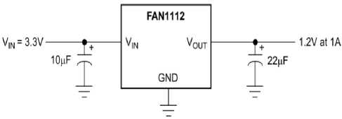
Fig. 6: Typical application of FAN1112 Regulator
-
B. Voltage 2.5V
For a product this voltage we use LD1117 0.5A, 2.5V series low drop fixed and adjustable positive voltage regulators. The LD1117 is a low drop voltage regulator able to provide up to 800mA of Output Current, available even in an adjustable version (Vref=1. 25V). Concerning fixed versions, are offered the following Output Voltages: 1.2V, 1.8V, 2.5V, 2.85V, 3.0V, 3.3V and 5.0V. We use fixed output voltage 2.5V. In Fig.7 shown Application circuit (for fixed output voltages).
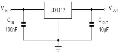
Fig. 7: Application circuit for fixed output voltages of LD1117 Regulator
-
C. Voltage 3.3V
For a product this voltage we use LD1086D2T33, 1.5A low drop positive voltage regulator adjustable and fixed The LD1086 is a low drop Voltage Regulator able to provide up to 1.5A of Output Current. Dropout is guaranteed at a maximum of 3.3V at the maximum output current, decreasing at lower loads. The LD1086 is pin to pin compatible with the older 3-terminal adjustable regulators, but has better performances in term of drop and output tolerance. In Fig.8 shown Application circuit (for fixed output voltages).
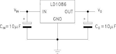
Fig.8: Application circuit for fixed output voltages of LD1086D2T33 regulator
The block diagram of proposed board is shown in Fig. 9.
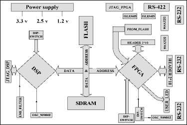
Fig. 9: Block diagram of proposed embedded board
-
V. DESIGN OF PCB FOR THE PROPOSED EMBEDDED BOARD
For some designers, as explained in [18], the PCB design will be a natural and easy extension of the design process. But for many others the process of designing and laying out a PCB can be a very daunting task. There are even very experienced circuit designers who know very little about PCB design, Proper PCB design is very often an integral part of a design. In many designs (high speed digital, low level analog and RF to name a few) the PCB layout may make or break the operation and electrical performance of the design. It must be remembered that PCB traces have resistance, inductance, and capacitance, just like your circuit does and as such leave it up to the "expert" specialist PCB designers. Design guidelines to be discussed concern radiofrequency (RF) noise from the microcomputer. This noise is generated inside the device and is coupled out in many different possible ways. The noise is present on all outputs, inputs, power supply, and ground at all times. Potentially, every pin on the microcomputer can be a problem. The biggest problem is noise from the integrated-circuit (IC) input/output (I/O) pins. Because the area covered with traces connected to them on the PCB from a large antenna. These pins also connect to both internal and external cables. The noise from clock switching within the IC appears as ‘‘glitches” on a static output. The glitch is caused by the common impedance of the output pin and the clock drivers, that is, the shared pins that supply each power and ground. The synchronous nature of most devices causes all currentswitching events to occur at the same time, making a large noise spike containing RF energy. The second most-important contributor is the power-supply system, which includes the voltage regulation and the bypassing capacitors at both the regulator and at the microcomputer. These circuits are the source of all the RF energy in the system, as they feed the clocked circuits inside the IC with the current required for switching. The third noise source is the oscillator circuit, where the oscillator swings rail to rail. In addition to the fundamental frequency, harmonics are introduced on the output side because the output buffer is digital, which squares the sine wave. Also, any noise caused by internal operations, such as the clock buffers, appears in the output. If proper separation is maintained between the crystal and its tank circuits from other components and traces on the PCB, and the loop areas are kept small, there should be no problems with this noise source. But it has been shown that if ICs or passive components, such as the main VBatt series inductor, are placed close to the crystal, harmonics of the crystal can couple and propagate [18]. We use total of available techniques in different references we try, for decoupling capacitors (bay pass) mount these strictly below the DSP and FPGA in the bottom layer of the board, because they should be placed as close as possible to the power supply pins DSP and FPGA. Also oscillators 50MHz placed as close as possible to DSP and FPGA. Particularly about DSP that must SMT EMI-Filter and oscillator 50MHz mount in one side of board near DSP. We for design PCB of the proposed embedded board use different techniques until noise reduced and achieve to a proper design. There techniques are described in below:
-
A. Microcomputer Grounds
A microcomputer ground is a ground area on the bottom layer underneath the microcomputer that becomes a ground island for the noise made by the microcomputer. This area should extend about 1/4 inch outside the outline of the device and tie to the microprocessor ground. Ground connections for the power-supply bypassing capacitors and any bypassing capacitors on the pins also should tie to this ground. Additionally, the ground area should extend out and around the through holes for the oscillator leads, and the bypass capacitors tied in to provide the smallest possible loop area when viewed from the Top. The top side traces are shown in the dotted line form on the bottom side diagram for alignment purposes. Notice how the oscillator capacitors lay back over the traces between the device and the crystal. This eliminates loop area. The same is true for the placement of the ferrite bead and V cc bypass capacitor, being centrally located with the main power lead running almost directly under the lead finger to the ground [19]. Thus we use microcomputer ground in bottom layer strictly below ICs DSP and FPGA about these ICs and decoupling capacitors (bypass) for the DSP and FPGA. In Fig. 10 proposed microcomputer ground is shown.
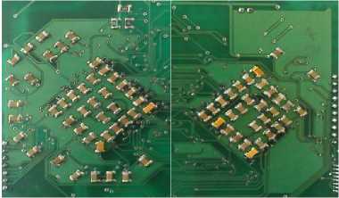
Fig. 10: Proposed microcomputer Ground for DSP and FPGA about these ICs and decoupling capacitors (bypass).
-
B. GND Polygon Layer by Total Top Layer
Grounding is fundamental to the operation of many circuits. Good or bad grounding techniques can make or break your design. There are several grounding techniques which are always good practices to incorporate into any design [18].
-
1) Use multiple visas to decrease your trace impedance to ground.
-
2) “Stitch” required points straight through to your ground plane, don’t use any more track length than you need.
-
3) Use copper, and lots of it. The more copper you have in your ground path, the lower the impedance. This is highly desirable for many electrical reasons. Use polygon fills and planes where possible.
-
4) Run separate ground paths for critical parts of your circuit, back to the main filter capacitor(s). This is known as “star” grounding, because the ground tracks all run out from a central point, often looking like a star. In fact, try and do this as a matter of course, even if your components aren’t critical. Separate ground lines keep current and noise from one component from affecting other components.
We in total of top layer use GND polygon layers to make a good GND chassis for power supply.
-
C. Board Zoning
Board zoning has the same basic meaning as board floor planning, which is the process of defining the general location of components on the blank PCB before drawing in any traces. Board zoning goes a little bit further in that it includes the process of placing like functions on a board in the same general area, as opposed to mixing them together (see Fig. 11). Highspeed logic, including micros, is placed close to the power supply, with slower components located farther away, and analog components even further still. With this arrangement, the high-speed logic has less chance to pollute other signal traces. It is especially important that oscillator tank loops are located away from analog circuits, low-speed signals, and connectors. This applies both to the board, and the space inside the box containing the board. Do not design in cable assemblies that fold over the oscillator or the microcomputer after final assembly, because they can pick up noise and carry it elsewhere [19]. We use board zoning technique for month total elements on proposed board.
PROPOSED EMBEDDED BOARD
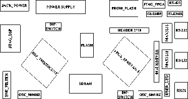
Fig.11: Board zoning as to proposed embedded board.
The real form of proposed embedded board, is shown in Fig.12.
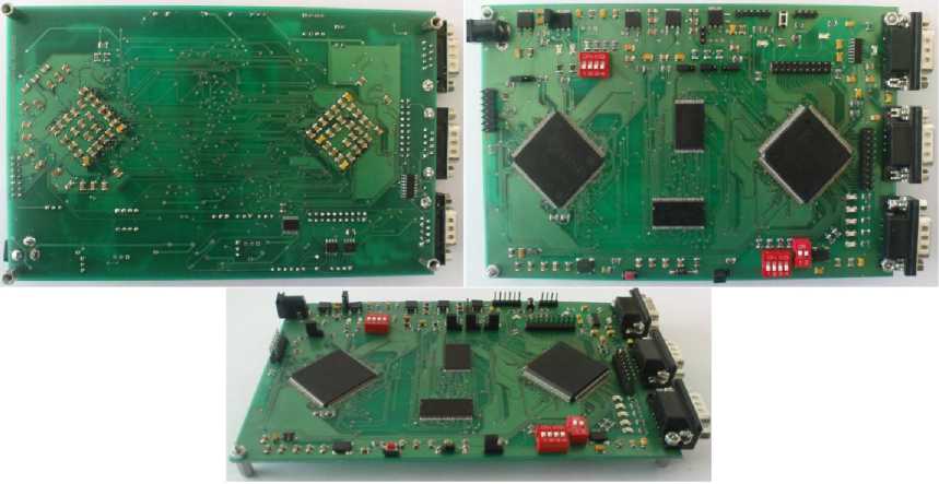
Fig.12: Real photo of the proposed embedded board, bottom of the board left of Figure and top of board is in right of Figure.
-
VI. COMPARISON
Characteristics of embedded systems are that these systems should be capable of real-time processing, have a light weight, have a lower cost, flexibility and ability to be reconfigured, and have convenient and effective communication with peripheral devices. Even though embedded computers have stringent requirements, cost is almost always an issue. We tried as much as possible in the design proposed board made small until to reduce costs. In this embedded board we have been used of both two DSP and FPGA technologies so compared to other designs that typically use only one technology DSP or FPGA. Other points that have been used in board design include design proposed board based on two layers , unlike commercial available boards that are made in several layers the terms of the construction costs are very expensive the components installed on both sides of the proposed board. The portable system weighing system may become a critical issue therefore we have designed the embedded board with very low weight and perfect for portable systems. Different companies do not report more details of their designed boards. In continue of this section compare different characters of the proposed embedded board with other related board. TABLE I shows characters of boards include dimension of boards, the number of layers, weight of boards, and peripheral connectors.
TABLE I: CHARACTERS OF DIFFERENT BOARDS INCLUDE DIMENSION OF BOARDS, THE NUMBER OF LAYERS, WEIGHT OF BOARDS, AND PERIPHERAL CONNECTORS.
|
Board |
Dimension( mm) |
Number of layers |
Weight(gr) |
Number of RS232 |
Number of RS422 |
|
[2] |
47.5*40.5 |
--- |
14 |
--- |
--- |
|
[3] |
50*40 |
--- |
16 |
--- |
--- |
|
[4] |
68*48 |
--- |
--- |
--- |
--- |
|
[5] |
--- |
--- |
--- |
1 |
--- |
|
[7] |
80*55 |
4 |
--- |
1 |
--- |
|
[8] |
98 * 67-120*67 |
--- |
--- |
1 |
--- |
|
[9] |
--- |
12 |
--- |
1 |
--- |
Fig. 13 shows figures of test and experimentation of actual hardware proposed embedded board.
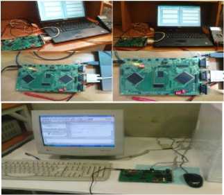
Fig.13: Figures of test and experimentation of actual hardware proposed embedded board.
-
VII. CONCLUSION
In this paper, a new low-cost and minimum embedded board based on TMS320C6713 (PYP) DSP and Spartan-3 XCS400-4PQG208C FPGA in two layers and mount elements in two sides of board for processing different digital algorithm and data an acquisition of sensors with serial port is presented. The aims of the proposed design were developments in low-cost embedded system design, and to explore board-level rapid prototyping using FPGA and DSP and also moreover low-cost properties can implement different type applications on proposed embedded board. In order to meet the requirements of miniaturization, low power of the system, all logic control communications and data cache interface circuit have been integrated in FPGA, these circuits including UART protocol, SPI protocol, glue logic, control units, other digital circuits proportional for a particular application. Approaches, which are used for reduces of size board and cost are included to mount the elements on two sides of the board, use ICs with multiple internal modular, using simple IC and circuits for power supply, use optimal of the total surface board for mounting elements as regards board zoning. We test proposed embedded board for different applications to understanding the software and hardware aspects of new low-cost and minimum embedded board, that result has been satisfactory and successful.
References A Two Layers Novel Low-Cost and Optimized Embedded Board Based on TMS320C6713 DSP and Spartan-3 FPGA
- Bhavya Daya, “Rapid Prototyping Of Embedded Systems Using Field Programmable Gate Arrays”, Bachelor of Science In Electrical Engineering, Spring 2009.
- http://www.trenz-electronic.de/, Trenz Electronic TE0630 Series.
- http://www.trenz-electronic.de/, Trenz Electronic GigaBee XC6SLX Series.
- http://www.trenz-electronic.de/, Trenz Electronic TE0320 (Spartan-3A DSP) Industrial Micromodule.
- www.quickembed.com, guikembed technology Co, TMS320C6713 and EP2C5.
- www.ourselec.com, Beijing OURS Electronic TechnologyCo.
- http://dlharmon.com/dspcard.
- http://www.traquair.com/products/microline.
- www.xilinx.com, “Spartan-3A DSP Starter Platform User Guide”, UG454 (v1.1) January 30, 2009.
- www.altera.com, “Cyclone II DSP Development Board Reference Manual”, Document Version: 6.0.1, August 2006.
- Louis N. Bélanger, “The advantages of using a combination of DSP’s and FPGA’s”, Lyrtech Inc, May, 2004.
- “TMS320C6713B Floating Point Digital Signal Processor”, SPRS294B − OCTOBER 2005 − REVISED JUNE 2006.
- Intersil, “3.3V, Low Power, High Speed or Slew Rate Limited, RS-485/RS-422 Transceivers”, data sheet, August 2004.
- Application Note: XC18V00, and Platform Flash PROMs; Spartan-II, Spartan-3, Virtex, and Virtex-II FPGA Families, “Reading User Data from Configuration PROMs”, XAPP694 (v1.1.1) November 19, 2007.
- “Spartan-3 FPGA Family Data Sheet”, DS099 December 4, 2009.
- David Bell, Scott Chen, “TMS320C6000: Board Design for JTAG”, SPRA584C - April 2002.
- David Bell, “TMS320C6000 Board Design: Considerations for Debug”, SPRA523C - April 2004.
- David L. Jones, “PCB Design Tutorial”, June 29th 2004.
- Texas Instruments, “PCB Design Guidelines For Reduced EMI”, SZZA009 November 1999.
