About the dynamics of some methods of integrating conversion of analog signal into digital code

Author: Tsytovich L.I., Dudkin M.M., Lokhov S.P., Brylina O.G.
Journal: Вестник Южно-Уральского государственного университета. Серия: Энергетика @vestnik-susu-power
Section: Устройства аналоговой и цифровой электроники
Article in issue: 1 т.13, 2013.
Free access
The new principles of constructing of the clocked reversible integrating analog-to-digital converters (ADCs) with pulse-width (PWM) and in-phase amplitude-frequency-pulse modulation (AFPM), as well as closed integrating ADC with tactless bit-by-bit equilibration is considered. The block diagrams and time diagrams of the ADC are reduced. An analysis of their dynamic characteristics is given. It is shown that the expansion of bandwidth of the ADC with PWM is possible by increasing the number of cycles of sweep conversion "within" the synchronization interval. In particular, it is proved the ADC with inphase AFPM in comparison with the known technical solutions has at least an order higher temperature and time stability of the characteristics. The bandwidth of the closed integrating ADC with tactless bit-by-bit equilibration depends on the time constant of channel integration. Significant expansion of the ADC bandwidth which purchased due to the reducing of the metrological characteristics is possible in his open-loop structure in the deficiency of channel integration.
Integrating analog-digital converter, integrating sweep converter, voltage converter into frequency of pulses, pulse-width modulation, amplitude-frequency-pulse modulation, tactless bit-by-bit equilibration, noise immunity, control system
Short address: https://sciup.org/147158227
IDR: 147158227 | UDC: 62
О динамике некоторых способов интегрирующего преобразования аналогового сигнала в цифровой код
Рассмотрены новые принципы построения тактируемых реверсивных интегрирующих аналого-цифровых преобразователей (АЦП) с широтно-импульсной (ШИМ), синфазной амплитудно-частотно-импульсной модуляцией (АЧИМ), а также замкнутого интегрирующего АЦП с бестактовым поразрядным уравновешиванием. Приведены структурные схемы и временные диаграммы сигналов АЦП, дан анализ их динамических характеристик. Показано, что расширение полосы пропускания АЦП с ШИМ возможно за счет увеличения числа циклов развертывающего преобразования «внутри» интервала синхронизации. В частности, доказано, что АЦП с синфазной АЧИМ по сравнению с известными техническими решениями имеет не менее, чем на порядок более высокую температурную и временную стабильность характеристик. Полоса пропускания в замкнутом интегрирующем АЦП с бестактовым поразрядным уравновешиванием зависит только от постоянной времени канала интегрирования. Значительное расширение полосы пропускания АЦП, приобретаемого ценой снижения метрологических характеристик, возможно в его разомкнутой структуре при отсутствии канала интегрирования.
Text of the scientific article About the dynamics of some methods of integrating conversion of analog signal into digital code
In control systems (CS) with the slave network of power valve converters (VC) [1–4] limit bandwidth fb is determined by the frequency fS and the number "m" of phase power supply and according to A. Kotelnikov theorem is f b ≤ 0,5 ⋅ m ⋅ f S [5]. Under these conditions, the clock frequency removal of data from analog-to-digital converters (ADCs) to choose the higher of those values that are dictated by the discreteness of VC is not only pointless, but harmful, so as it leads to a decrease in noise-immunity of control system due to "entering" of high-frequency pulsation [6] determined by the properties of the converted analog signal into a digital code. These coordinates are, for example, the signals of the current and voltage feedback, and in some cases, the rate of the actuating mechanism, as well as external noises, which are often the generator directly to the elements of the electronic part of the CS, working in a discrete (pulsed) mode [7] 1 .
To date, more effective ways to increase the noise immunity of the ADC than integrating analogdigital conversion, not invented. The leaders are ADC with push-pull integration [8, 9], the ADC with integrating pulse-width modulation (PWM) [10] and number-to-pulse ADC [9].
The basic disadvantage of the ADC with pushpull integration is interval when the ADC’s input is disconnected from the source of the converted signal and the CS is actually loses connection with the processes that occur in it. The only way to avoid a similar situation is used in a bundle of two antiphase running the ADC, which complicates not only the whole construction of the ADC, but also its setting.
The basis of the ADC with PWM are integrating sweep converters (SC), which synchronized external sawtooth or pulse signal. The processes in these ADCs are aperiodic mode, depending on the parameters of the synchronization signal and the time constant of SC’s integration circuit [11] and, as a rule, are rather inertial, to be used in fast CS.
In the number-pulse ADC are made rigid requirements on the work stability of the converter of input signal into frequency of pulses, which added task of supplying the reversibility of the ADC that is his ability to work with the signals of both positive and negative polarity.
The overall quality of the referred ADCs is open character of their structure, which gives to rise the natural problem of providing a high level of metrological characteristics of the converter, and the need for clock interval of the ADC, after which the command is issued to permit data reading. Often the clock period is dictated by the most inertial link of the ADC, which determines the dynamics of this method of analogdigital conversion. Usually, when solving the traditional problems of automation, the fact of the ADC clock is not negative, in some cases, it is an effective means of suppressing noise [7]. However, optimization of dynamic characteristics of objects with non-stationary parameters and a high level of external noise is desirable to have the tactless integrating ADC, allowing the system to change the sampling frequency, depending on its mode.
The purpose of the article is acquaintance of specialists in the field of information electronics and automation of technological processes, as well as the manufacturers of integrated circuits with the developments in the field of ADCs, which have been made in recent years in the department of electric driver of SUSU and are intended for control systems by valve electric drives and technology automation [12–14], characterized by high levels of interfering signals.
Clocked ADC with integrating PWM
ADC (Fig. 1 a) contains the SC, the generator of signal of sawtooth sweep GSS and converter "PWM – DIGIT".
The SC [11] includes an adder Σ, an integrator with a transfer function W(p ) = 1 / T I p , where T I is time constant and the anhysteresis relay element RE with symmetric no inverting characteristic, the output signal which varies discretely within ± A .
"Inside" the GSS of a counting circuit (in fig.1 a isn’t shown) is formed digital reference sawtooth
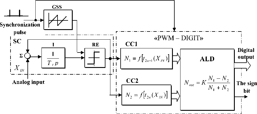
Fig. 1. Block diagram (a) and timing diagrams of signals (b – e) of the reverse integrating analog-to-digital converter with a PWM
sweep (Fig. 1 b), period T S of which is determined by the external clock pulses corresponding to the sampling interval of the VC.
The discreteness of reference sweep is determined by the frequency of own generator of counting pulses and is negligible quantity. With help the sweep are given numbers N 1*, N 2*, N 3*, ..., Nk * so that they followed with a period T 0< TS , where TS / T 0 = n – an integer. In Fig. 1 b as an example, there are three values N 1*, N 2*, N 3* , which form a discrete front of GSS’s output analog sweep destined for synchronization of SC.
Switching the REs occurs at instant times, when equal amplitudes of the signals of the master sweep to the GSS’s output and slave sweep from the output of the integrator I. If the input signal Х in is, for example, negative polarity (Fig. 1 c), then on the time interval t 1 the signal of the master sweep from the output of the integrator I equal difference of the signal at the output of RE and the input signal of SC ( A – Х in ), and in the interval t 2 it equal add of these signals (– A – Х in ) (Fig. 1 с, e).
As a result, t 1 > t 2, and the average value of the output pulses of REs is proportional to the input signal Xin . With the positive input signal SC works similarly with the only difference is that t 1< t 2.
In general, the SC synchronized of "saw" on the output of RE is an aperiodic link W(p ) = 1/(1 + T E p ) [11], where TE « 0,45 • T I • T 0 is the equivalent time constant of the SC; T I = T I I T GSS is normalized value of the integrator time constant I referred to the time constant of the signal of sawtooth sweep TGSS . In general, Т 0 = Т S / n , where n is the division factor of synchronization interval T S (Fig. 1 b – e). At that, the condition Т I > 2 Т GSS should comply for reliable synchronization of SC by signal from the output of GSS.
From these relations it is clear that as the period of the sawtooth sweep signal T 0 "inside" synchronization interval decreases so speed of SC increases.
Converter "PWM – DIGIT" (Fig. 1 a) contains two counting channels CC1, CC2 and arithmetic-logic device ALD. CC1 converts into a digital code N 1 pulses of positive polarity, and CC2 forms a code of N 2, depending on the duration of the output pulses of negative polarity.
In this case, are the following options of "numbering" of the PWM signal from the output of the SC.
In the first case it is assumed that on the interval Ts (Fig. 1 b) sum of "odd" N 1 ^t 2 i - 1 and "even" i = 1 n
N 2 = ^ 1 2 i synchronization intervals of SC (Fig. 1 d) i = 1
are converted to "digit" with following calculation of N -N the output code NouT = К —1----2, where K is the
OUT N 1 + N 2
coefficient of scheme proportionality.
The second option of converting of analog signal into the code takes into account only the latest in a series of periods when N1 = 12n-1, N2 = 12n and N - N
N ouт = К —1----2. In either case, the sign bit is
OUT N 1 + N 2
formed in ALD by comparing the values of N 1 and N 2 .
In Fig. 2 shows the logarithmic amplitudefrequency characteristics (LAFC) k = F(f ) of ADC with PWM, taken at different values of the division factor n = ТS / Т 0 of the synchronization interval TS and the relative integration time constant of SC T I = 2,2 for the first (Fig. 2 a) and the second (Fig. 2 b) algorithms of "numbering" of the PWM signal are "inside" of the synchronization interval T S . Here, k is a coefficient of transmission of an integrating ADC; f = f iN I f S is normalized frequency fIN of the harmonic input signal divided by the frequency of clock pulses fS = ( T S ) - 1 ( TS = 3,3 ms). LAFC obtained by modeling of the ADCs in a technical computing software MatLab + Simulink.
LAFC analysis showed the following:
-
- an increase in the number " n " sampling intervals T 0 "inside" the synchronization interval T S of VC leads to the expansion of ADC’s bandwidth due to the to reduce the equivalent time constant of the T E of SC (Fig. 2 a). For example, for n = 1 a range of uniform bandwidth of ADCs frequency is at the level f ® 0,17 and for n = 8 is f ~ 0,4 ;
-
- slight difference between the LAFCs for n = 4 and n = 8 shows that the rational value of the coefficient " n " be considered as n = 4, when a compromise is possible between the dynamics and noise-immunity of the ADC;
-
- "numbering" of the PWM signal from a finite sampling interval a series of SC’s output pulses (Fig. 2 b) can increase the bandwidth of the ADC as compared to the initial method of converting of PWM signal into a digital code (Fig. 2 a). For example, if the "numbering" is not a series of pulses, but only a finite sampling interval (period), then for n = 4 bandwidth of the ADC (Fig. 2 a) increases almost to the limit value f » 0,5 (Fig. 2 b).
This is explained as follows. So under the influence of the input step waveform (Fig. 3 a), SC goes on the desired trajectory to exponentially when each of the sampling intervals T 01 ... T 0 n (Fig. 3 b) contains the error Δ1 ... Δ n (Fig. 3 c). Obviously, the error of the last of a series of sampling intervals will be the lowest in comparison, for example, with an average resulting error of the SC [ 5 = ( S A i )I n ] > A n for the entire sampling interval TS of VC.
Clocked ADC with in-phase amplitudefrequency-pulse modulation (AFPM)
This class of ADCs [15] is advisable to apply in cases where a wide dynamic range of the converted
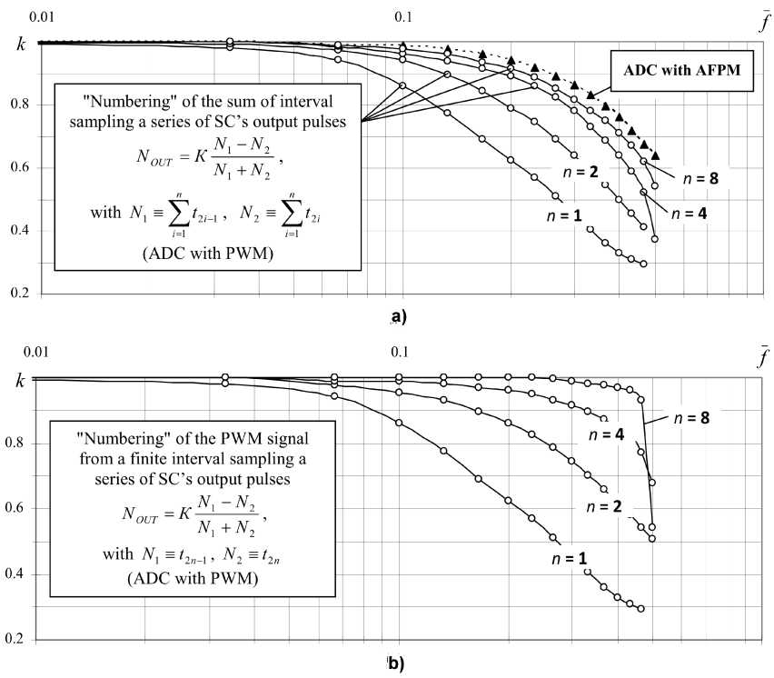
Fig. 2. The logarithmic amplitude-frequency characteristics (LAFC) k = F(f) of integrating ADC with PWM in different ways of ‘numbering’ of PWM signal (a, b) and LAFC of ADC with in-phase AFPM
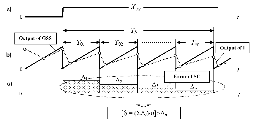
Fig. 3. The timing diagrams of signals to the analysis of the error of ADC with PWM
signal must be combined with high temperature stability characteristics of the analog-digital converter.
ADC (Fig. 4 a) contains two identical on his action integrating a voltage converter into frequency of pulses VCF1 and VCF2 [16, 17], containing amplitude modulators AM1, AM2, adders Σ1, Σ2, integrators I1, I2 and relay elements RE1, RE2.
Each of the VCF is intended for work with the signal of a certain polarity. So VCF1 transforms the input voltage of positive polarity into frequency of pulses, and VCF2 transforms input signal of negative polarity.
In the absence of a signal X IN on the ADC’s information input (Fig. 4 b), the output voltage of AM1
and AM2 are zero, so the blocks Σ1, I1, RE1 and Σ2, I2, RE2 operate in a free-running mode when the outputs of RE1 (Fig. 4 d) and RE2 (Fig. 4 e) are formed bipolar pulses with frequency f 0 = ( Т 0) - 1 . If links characteristics of channels VCF1, VCF2 are identity, then its work with an equal value of the initial frequency f 0 .
A possible phase shift between output signals of VCF1 and VCF2 principle does not matter, since it might ultimately lead to a conversion error only to one significant digit of binary code.
The output signals of the integrators I1, I2 are symmetric sawtooth wave shape and are limited in amplitude of switching thresholds ± b of RE1 and RE2 (Fig. 4 d, e).
When applied to the ADC input signal is positive (Fig. 4 b) then at the input of AM1 appears positive sign voltage, which is then converted into frequency of output pulses of RE1, which increases in proportion to the amplitude of the XIN due to in-phase of output pulses of AM1 and RE1 (in-phase AFPM) (Fig. 4 c, d). At the same time VCF2 works in a free-running mode with an initial frequency equal f0, acting as a channel of the reference frequency.
In general relations (1) are valid for VCF1 and VCF2.
' 1 2 n - 1 = 1 2 n = 0,5 7 0/ (1 + X in ); _
T n = 1 2 n - 1 + 1 2 n = 0,5 T c/ (1 + X in );
< T O = T o , n\X iN = 0 = 4 bT ; Tout = T O/ T 0, n = 1 + Xin ;(1)
ч b = bl a; ; Xin = Xin/A ; n = 1, 2, 3, - where fOUT – the normalized frequency of the output pulses of VCF1 and VCF2 respectively; Х IN , b – the normalized value of the ADC input signal and switching thresholds ±b of RE1, RE2, respectively; TI - time constant of the integrators I1, I2; ±A - the amplitude of the output pulses of RE1, RE2. At the same time b < 1,0 and the value of Х IN can be arbi-
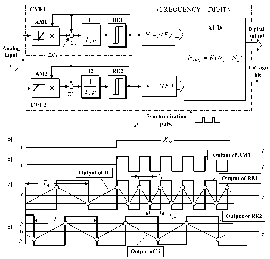
Fig. 4. Block diagram (a) and timing diagrams of signals (b – e) of the reverse integrating ADC with in-phase AFPM
trarily large from the theoretical positions, as well as the frequency of the output pulses of VCF.
Further transformation of impulses frequency into a digital code is done using the channel "FREQUENCY – DIGIT" (Fig. 4 a), where CC1 forms the number of N 1, proportional to the frequency of the output pulses of VCF1 and CC2 forms the number of N 2, depending on the frequency of the output signal of VCF2.
The resulting code of ALU N OUT = К • ( N 1 - N 2 ) is passed to output buses of the ADC at time of formation of the synchronization pulse and saved on them until the end of the next conversion cycle. Sign bit is also obtained by comparing the values of N 1 and N 2.
Analysis of dynamic characteristics of the ADC with AFPM showed that the determining factor here is the frequency of synchronization pulses, and from the frequency of self-oscillations of VCF1, VCF2 depends only on the ADC`s digit, that is, the sampling error on the level of the converted signal.
Logarithmic amplitude-frequency characteristics of the ADC with AFPM is shown in Fig. 2 a, which was read at an initial frequency of the output pulses of VCF1, VCF2 equal to f 0 = 10 kHz. The results show that the dynamic property, this class of the ADC, occupies an intermediate position between the ADC-PWM with an integer division of the sampling interval (Fig. 2 a) and ADC-PWM, where the "numbering" is made on the last sampling interval of SC (Fig. 2 b).
The using of VCF with in-phase AFPM can significantly improve the temporal and thermal stability of characteristics of the ADC.
So in the case drift of "zero" signal A e z of I or AM, for example, positive polarity (relations (2)), the interval t 2 n - 1 (Fig. 2) of the output pulses of RE1 is reduced, and the interval t 2 n is increasing. In this case the resulting error A f OUT of the frequency of output pulses is proportional to A e 2 , while for the traditional
structures of VCF [10] is A f = A e
e t2 n-1
2 bT i . t e = 2 bT i ;
1 + XIN — A е ] 1 + XIN +A е ]
f^ = ( t ъ — 1 + 1t ) - 1
1 + Х1М
•
4 bТI
—
A e y
(1 + X in ) 2
5 f our
= 1
-
f OeUT
fOUT(4e S = 0 )
A e] .
(1 + X in ) 2 ;
Ae =
Aе2
А
; b =
b
A
; Х IN =
Х IN А
The system of equations (2) except for the previously adopted the following notation: A e ^ is normalized value of the resulting drift of "zero" signal of the integrator I1 (I2) and the amplitude modulator AM1 (AM2) is provided to input of the adder Σ1 (Σ2) (Fig.
4 a); 5 f e UT is the relative error of the frequency of output pulses of VCF in the presence of signal A e ^ .
Given that A e ^ <<1,0, considered the VCF has the temperature and time stability of characteristics of the at least one order of magnitude greater than the known technical solutions.
As shown by experimental research, when the channels VCF1 and VCF2 based on the same hardware components of a series then their resulting drift of the "zero" is the almost identical in sign and magnitude. Then each of the codes N 1 and N 2 contain the same component of the error of “zero” A N , which in practice provides a partial self-correction result of the conversion N 1 – N 2.
Closed integrating ADCwith tactless bit-by-bit equilibration
The integrating ADC with tactless bit-by-bit equilibration [18–20] with a built in its closed circuit digital-to-analog converter (hereinafter "ADC – DAC") (Fig. 5) contains adders Σ IN , Σ 2 n –1 ... Σ 2 n –3 and Σ OUT , integrator I, relay elements RE1 ... RE n and proportional links P1 ... Pn. When considering the principle of the ADC–DAC is limited to four digits " n " of binary code.
Links Σ IN , Σ2 n –1, ... , Σ2 n –3, I, RE1 ... RE n combine to form the ADC. Functions of the DAC operates the proportional links P1 ... Pn and Σ OUT . Adders Σ IN , Σ2 n –1 ... Σ 2 n –3 have a unit coefficient of transmission for each of the inputs and produce the subtraction of input signals. The relay elements RE1 ... RE n generally have symmetrical with respect to "zero" hysteresis loop, and their output signal changes discretely within ± A .
The adder Σ OUT has " n " number of inputs with a unit coefficient of transmission for each of them and makes a summation of the signals. Number of inputs the adder is chosen equal to the number of digits " n " of the converted binary code.
Proportional links P1 ... P n are implemented with coefficient of transmission, which are varied according to bit’s weight of the converted code in the general case with arbitrary base, but more often, as taken here, with a binary code which is the proportional to series 2 n –1 , 2 n –2 , ..., 2 0 . The largest coefficient of proportional link 2 n –1 corresponds to the weight of high-order bit of binary code, and the lowest 2 0 corresponds to the weight of lower order bit.
Further in the text use the following notation: YI is the output signal of the integrator I, YOUT is the output signal of the adder S OUT ; ± A - 2 n -1 , ± A - 2 n -2 , ± A - 2 n -3 , ... , ± A • 2° are the maximum levels of output signals of proportional links P1 ... P n , respectively; ± b are switching thresholds of RE1 ... RE n , with | b | < | А |; ± А is the amplitude of the output pulses of the relay elements RE1 ... RE n , and believe that the level "+ A " corresponds to a logical "1", and the level "– A " corresponds to a logical "0"; Q n –1 , Q n –2 , Q n –3 , ..., Q 0 are bits of digital output code at the outputs of the RE1 ...
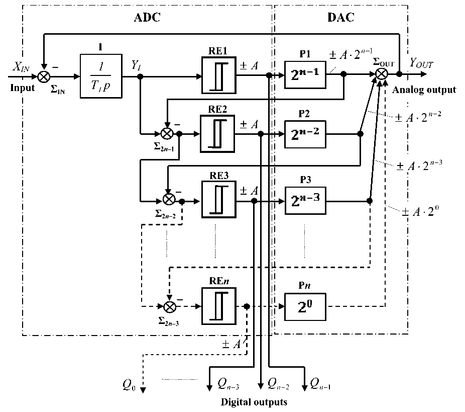
Fig. 5. The block diagram of closed-integrating ADC with tactless bit-by-bit equilibration
RE n ; N 1 is digital code at the output of the RE1 ... RE n .
For ADC – DAC input signal can be represented in the form of expression XIN = ±A(k + 0,5m), where A = 2A N = 2 A is the weight of the unit of maх max lower-order bit of the converted code in analog form;
i = n - 1
N = У 2i = 2n -1 is the maximum value of a max i=0
binary digital code in decimal, which is formed at the outputs of RE1 ... R n ; А = A max/ N max is the pulse’s amplitude at the output of relay elements RE1 … RE n , A max is the maximum amplitude of the output signal of the DAC k = 0, 1, 2, ... , ( N max -1)/2 are whole numbers, corresponding decimal numbers of the converted code; m is coefficient taking into account changes of the input signal in the interval A ( - 1,0 < m < 1,0).
Consider the operation of the device, provided XIN = 0, when numbers k = 0 and m = 0.
We assume that the relay element RE1, which forms the high-order bit of the converted code is in the
+ A . Then the amplitude on the output of proportional link P1 is А-2n -1 . For the equality X IN = Y OUT , all the rest RE2 … RE n in the system are forced to switch to the "negative" position when the summary output signal 2 out is Y ou = А ( 2 n - 1 - 2 n - 2 - 2 n - 3 - ,..., - 20 ) = A . The condition that X IN = Y OUT is impossible for the case X IN = 0, so that the signal at the output of the integrator I will fall under the action of voltage – A from the output Σ IN , and where the equality Y I = – b is achieved then first RE1 goes into "negative" state, and RE2 ... RE n go in "+ A ". As a result, the summary output signal Σ OUT corresponds a value Y OUT = А ( - 2 n - 1 + 2 n - 2 + 2 n - 3 - ,..., + 20 ) = - A .
Thus, for X IN = 0 ADC – DAC is always in the mode switch of all relay elements with carrier oscillation frequency f 0 = 1j ( 4 bT I ) , where b = | bl A | is the normalized value of switching threshold of RE1 ... RE n ; T I is time constant of integration.
As a result with XIN = 0 at the output of RE1 ... REn periodically formed two values of shifted binary code N1, which are equal to: (Nmax +1)/2 and (Nmax -1)/2 . To bring it to the standard form necessary from the code value N1 subtract the value N2 = (Nmax +1)/2 . The latter is implemented by the device of subtracting codes (in Fig. 5 is not shown to simplify the circuit ADC – DAC). Then, for XIN = 0 the output code of converter N3 = N1 – N2 in decimal form will be equal zero or minus one. As a result, the output of the ADC is formed by a static error which is equal to one lower order bit. With a large number of digits of ADC - DAC (n > 8) the error is almost no noticeable effect on the accuracy of his work and can be neglected.
For other values of k * 0 and m = 0, ADC - DAC works similar to the case with numbers k = 0 and m = 0. In this case at least one of the relay elements RE1 ... RE n is necessarily in a mode of switching with a carrier frequency f 0 = 1J ( 4 bT I ) .
Consider the work of the converter for other values of m, different from zero and changing the range - 1,0 < m < 1,0 and k = 0 when X IN = ± А • m . For these values the device goes into a frequency-pulse-width modulation (FPWM), in which the switching frequency of RE1 ... RE n reduced in accordance with the expression f = f 0 ^ ( 1 - m 2 ) . The condition code N 1 on the output of RE1… RE n remains the same as for the case k = 0 and m = 0.
For m = 1 and any other integer values of k the switching frequency of RE1 ... RE n becomes equal zero and there is an established process in the converter, when X IN = Y OUT . For example, for X1 N = А ( k = 0) the relay element RE1 is switched to "positive" state, and RE2 ... RE n are switched in the "negative" position. As a result, the summary signal at the output of the DAC is Y OUT = А ( 2 n - 1 - 2 n - 2 - 2 n - 3 - ,..., - 2 0 ) = A and is balanced by the input signal X1N = А . The output voltage of the integrator I reaches a steady-state value YI ( t ) = b so as to constantly keep the RE1 in a "positive" state. Offset digital code N 1 at the output of RE1 ... RE n is equal value ( N max + 1)/2, and the code N 3 = 0.
Similarly, ADC – DAC operates at other values of k and m = 1. For example, the maximum possible value k = ( N max - 1)/2 will correspond the maximum
. (N™. 1 1)
input signal level X IN = ±AJ —max— + - I = ± А • N max .
If X IN = А • N max , then RE1 ... RE n switched to a state + A .
As a result, the summary output signal ΣOUT is equal to YOUT = А(2n-1 + 2n-2 + 2n-3+,..., + 20)= A• Nmx and is balanced of input signal XIN = А • Nmax. The output voltage of the integrator I reaches a steady-state value YI (t) = (Nmax -1) + b so as to constantly keep RE1 ... REn in "positive" state, which corresponds to the minimum value of the code N1 = 0. When you subtract from the code N1 to code N2 = (Nmax +1)/2 we get a code N3 = (Nmax +1)/2 on the converter output.
For X IN = - А • N max , conversely all the RE1 ... RE n are switched in "negative" state, when the output voltage Σ OUT changes sign and becomes, equal Y out =- А ( 2 n - 1 + 2 n - 2 + 2 n - 3 + ,... , + 2 0 ) = - A • N max , which corresponds to the minimum value of the code N 1 = 0. When you subtract from code N 1 to code N 2 = ( N max + 1)/2 we get a code N 3 =- ( N max + 1)/2 on the converter output.
The considered ADC – DAC is a closed system, so the steady-state mode the signal level X IN at the input of ADC must always be balanced by voltage output Y OUT of the DAC. When the digit capacity of DAC does not provide the desired accuracy (discrete) of transformation between levels, then between these levels starting mode of frequency-pulse-width modulation. However, the averaged integral accuracy is always ensured because of the integrator in the direct regulation channel.
In Fig. 6 shows the oscillograms of the four-digit integrating ADC – DAC, obtained on the basis of computer modeling in the program MatLab + Simu-link, when exposed to its input the dynamic signal X H (t ) = A m -sm(2 n f t ), where Аm , f are the amplitude and the frequency of the harmonic input signal, respectively.
Modeling was performed with the following parameters: the maximum amplitude at the output of the DAC is equal to A max = 15 V, the weight of the unit of lower bit order of converted code in analog form is equal to A = 2 А max/(2 n - 1) = 2 V, the amplitude of the pulses at the output of relay elements RE1 … RE4 are equal to А = А max/(2 n – 1) = 1, normalized switching thresholds of relay elements RE1 ... RE4 are equal to b = | b/'A | = 0,5, integration time constant of the integrator is equal to T I = 0,1 ms, the carrier oscillation frequency f 0 = 1J ( 4 bT I ) of converter by XIN = 0 is equal to 5 kHz.
From the oscillograms at the Fig. 6 can be seen that the output signal at the output of the DAC is divided into 15 modulation zones ( Z = 2 n – 1) according to the digit " n " of binary code. Within each modulation zone converter operates in the mode of FPWM, as a result, the average output signal Y 0( t ) of DAC with high accuracy reproduces the harmonic input waveshape XH ( t ) (Fig. 6 a, b). With increasing frequency f of input signal the mode of FPWM within each modulation zone disappears and at the device output is formed by a discrete signal (Fig. 6 c, d).
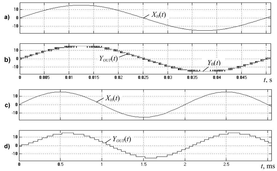
Fig. 6. Oscillograms of the four-digit integrating ADC – DAC with tactless bit-by-bit equilibration with A m = 15 V: f = 20 Hz (а, b) and f = 500 Hz (c, d)
In Fig. 7 shows the logarithmic amplitudefrequency characteristics (LAFC) k = F ( f ) for the eight-digit integrating ADC – DAC, where k = A OUT / Am is transfer constant of the ADC – DAC; AOUT is the amplitude of the output signal of the DAC; f is the frequency of the input harmonic signal Х H ( t ).
Analysis of the results showed that:
-
- the uniform bandpass f b of converter "Analog – digit – analog" in which the transmission coefficient k decreases in 2 times depends only on the integration time constant T I and does not depend on the level of the input harmonic signal ХH ( t ), the switching thresholds " b " of RE1 … RE n and bit " n " of the converter;
-
- for the chosen value of the normalized switching threshold of RE1 ... RE n b = \b! A\ =0,5 the relative bandwidth of the converter f b = fb/ f 0 is approximately 0,32 for all values of the integration time constant T I (Fig. 7), so that the normalized value of switching thresholds of RE1 ... RE n b = bl A\ should be chosen as close as possible to the unit, but don’t not equal to it. For example, if b = 0,9 and all values of T I the relative bandwidth reaches a value fb ® 0,57 that goes beyond the theoretically justified for pulsed systems the extent to which the interface between the frequency range of reliable and delayed sample is determined from Theorem of V.A. Kotelnikov and amounts f b < 0,5 . The results obtained are valid not
only for the eight-bit ADC, but also for the converters with any other digit.
In cases where the priority is the speed of the ADC, but not his noise immunity the integrator I should be replaced by a proportional amplifier (repeater) and the feedback from the output of the DAC to the input of the ADC should be removed.
Findings:
-
1. At control systems with the slave chain of power valve converters the clock period of integrating ADC with PWM and AFPM advisable to choose a discrete set to VC, which is determined by the number of phase voltage and the configuration of its power circuit.
-
2. Expanding bandpass of ADC with PWM, clocked synchronization signal of VC, is possible by increasing the number of cycles of the sweeping conversion "inside" of the synchronization interval. In this case the best result gives a method in which the "digitization" is not subject to the amount, and the last of a series of intervals of the sweeping conversion of the ADC on the discretization interval of the VC.
-
3. ADC with in-phase AFPM has a practically unlimited allowable range of input signal and increased thermal and temporal stability of the characteristics of more than similar solutions for at least an order of magnitude. The dynamic characteristics of this class ADC are determined by sampling interval of VC (cycle transformation).
-
4. First proposed a closed integrating ADCs with tactless bit-by-bit equilibration and bandwidth
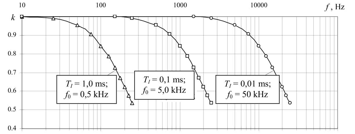
Fig. 7. The logarithmic amplitude-frequency characteristics of the eight-digit integrating ADC – DAC with tactless bit-by-bit equilibration with Аm = Am I A max = 1,0 (А max = 12,75 V, Δ = 0,1 В, А = 50 mV, b = 25 mV, Z = 255)
-
5. Increase speed the tactless ADCs is possible by changing the channel of integration to the proportional amplifier, with simultaneous breaking the feedback loop, which achieved at the cost of noise immunity and accuracy of the ADC.
depends only on the time constant of channel integration, which can be used in particular in control systems with variable cycle data collection and processing.
References About the dynamics of some methods of integrating conversion of analog signal into digital code
- Управление вентильными электроприводами постоянного тока/Е.Д. Лебедев, В.Е. Неймарк, М.Я. Пистрак, О.В. Слежановский. -М.: Энергия, 1970. -199 c.
- Пат. O346376 Российская Федерация, МПК H 02 K 19/24. Синхронная реактивная машина/Ю.С. Усынин, М.А. Григорьев, К.М. Виноградов, А.Н. Горожанкин, С.А. Чупин. -№ 2007126685; заявл. 12.07.07; опубл. 10.02.09, Бюл. № 4.
- Электропривод с синхронным реактивным двигателем независимого возбуждения/Ю.С. Усынин, Н.Д. Монюшко, Г.В. Караваев, М.А. Григорьев//Вестник ЮУрГУ. Серия «Энергетика». -2001. -Вып. 1. -№ 4(4). -С. 70-76.
- Удельные показатели электропривода с синхронным реактивным двигателем независимого возбуждения/Ю.С. Усынин, М.А. Григорьев, К.М. Виноградов, А.Н. Горожанкин//Вестник ЮУрГУ. Серия «Энергетика». -2008. -Вып. 9. -№ 11(111). -С. 52-53.
- Bissell, C. Vladimir Aleksandrovich Kotelnikov: pioneer of the sampling theorem, cryptography, optimal detection, planetary mapping.. History of Communications/C. Bissell//Communications Magazine. IEEE. -2009. -№ 10. -P. 24-32.
- Brinkis, K. The automated control of a power system/K. Brinkis, A. Staltmanis//Baltic electrical engineering revier. -1997. -№ 2(6). -P. 39-44.
- Осипов, О.И. Промышленные помехи и способы их подавления в вентильных электроприводах постоянного тока/О.И. Осипов, Ю.С. Усынин. -М.: Энергия, 1979. -80 с.
- Прянишников, В.А. Интегрирующие цифровые вольтметры постоянного тока/В.А. Прянишников. -Л.: Энергия, 1976. -315 с.
- Волович, Г.И. Схемотехника аналоговых и аналогово-цифровых электронных устройств/Г.И. Волович. -М.: Издательский дом «Додэка-XXI», 2005. -459 с.
- Мартяшин, А.И. Преобразователи электрических параметров для систем контроля и измерения/А.И. Мартяшин, Э.К. Шахов, В.М. Шляндин. -М.: Энергия, 1976. -390 с.
- Дудкин, М.М. Элементы информационной электроники систем управления вентильными преобразователями: монография/М.М. Дудкин, Л.И. Цытович. -Челябинск: Издательский центр ЮУрГУ, 2011. -362 с.
- Григорьев, М.А. Линейная плотность поверхностного тока в энергосберегающих электроприводах с синхронной реактивной машиной независимого возбуждения/М.А. Григорьев, А.Е. Бычков//Вестник ЮУрГУ. Серия «Энергетика». -2010. -Вып. 14. -№ 32(208). -C. 46-51.
- Развитие частотных методов синтеза электроприводов с синхронными электрическими машинами/Ю.С. Усынин, М.А. Григорьев, А.Н. Шишков и др.//Вестник ЮУрГУ. Серия «Энергетика». -2011. -Вып. 16. -№ 34(251). -C. 21-27.
- Частотные характеристики канала регулирования момента в синхронных электроприводах/Ю.С. Усынин, М.А. Григорьев, А.Н. Шишков//Электричество. -2012. -№ 4. -С. 54-59.
- Пат. 2429563 Российская Федерация, МПК7 Н 03 М 1/02. Реверсивный число-импульсный аналого-цифровой преобразователь/Л.И. Цытович, М.М. Дудкин, А.В. Качалов, Р.М. Рахматулин. -№ 2009147981/09; заявл. 23.12.09; опубл. 20.09.11, Бюл. № 26.
- Анализ динамики интегрирующего амплитудно-частотно-импульсного развертывающего преобразователя аналоговых сигналов в частоту импульсов/Л.И. Цытович, Р.Х. Гафиятуллин, Р.З. Хусаинов, М.М. Дудкин//Вестник ЮУрГУ. Серия «Энергетика». -2003. -Вып. 3. -№ 11(27). -С. 36-40.
- Интегрирующие развертывающие преобразователи с повышенной температурной стабильностью характеристик/Л.И. Цытович, М.М. Дудкин, А.В. Качалов и др.//Приборы и системы. Управление, контроль, диагностика. -2010. -№ 10. -С. 38-43.
- Пат. 2460210 Российская Федерация. МПК7 H 03 M 1/52. Интегрирующий преобразователь «Аналог -Цифра -Аналог»/С.П. Лохов, Л.И. Цытович, М.М. Дудкин, Р.М. Рахматуллин, О.Г. Брылина. -№ 2011125193/08; заявл. 17.06.11; опубл. 27.08.12, Бюл. № 24.
- Замкнутый интегрирующий аналого-цифровой преобразователь с бестактовым поразрядным уравновешиванием/С.П. Лохов, Л.И. Цытович, М.М. Дудкин и др.//Приборы и системы. Управление, контроль, диагностика. -2012. -№ 11. -С. 27-35.
- О новом принципе интегрирующего аналого-цифрового преобразования с бестактовым поразрядным уравновешиванием/С.П. Лохов, Л.И. Цытович, М.М. Дудкин и др.//Вестник ЮУрГУ. Серия «Энергетика». -2012. -Вып. 18. -№ 37 (296). -С. 97-106.
