About the possibility of the bulk thermo gradient effect use for the creation of the effective thermobattery

Author: Zhakatayev Toksan A.
Journal: Журнал Сибирского федерального университета. Серия: Техника и технологии @technologies-sfu
Article in issue: 1 т.13, 2020.
Free access
The theoretical basis has been developed and the idea of practical production and testing the semiconductor electric generator (thermobattery) of a new type acting on the basis of a metal - semiconductor system has been offered. It is shown that the thermobattery will work on the basis of the use of a bulk thermogradient effect. Such effect allows to gain a sufficient level of generated power from one unit of the whole volume of a semiconductor material. When using the semiconductor thermobattery together with solar and wind electric generators, it is possible to simplify significantly constructional and technological features of these installations.
Thermo, gradient, effect, e.m.f, semiconductors, impurity, battery
Short address: https://sciup.org/146281418
IDR: 146281418 | UDC: 537.311; | DOI: 10.17516/1999-494X-0202
О возможности использования объемного термоградиентного эффекта для создания эффективной термобатареи
Разработана теоретическая основа и предложена идея практического изготовления и испытания нового вида полупроводникового электрогенератора (термобатареи), действующего на основе системы металл - полупроводник. Показано, что термобатарея будет работать при использовании объемного (пространственного) термоградиентного эффекта. Данный эффект позволяет получить достаточный уровень генерирумой мощности с единицы объема полупроводникового материала. При использовании полупроводниковой термобатареи в комплексе с солнечными и ветровыми электрогенераторами можно существенно упростить конструкционные и технологические особенности этих установок.
Text of the scientific article About the possibility of the bulk thermo gradient effect use for the creation of the effective thermobattery
It is a widely known fact in science that the contacts of metal and semiconductor generate thermo electromotive force (e. m. f.) [1-12] (Fig. 1).
The interesting fact [1] is noted that during World War II between the USSR and fascist Germany (1941-1945), the Soviet guerrillas used the thermo power generator as a current source which was manufactured on the basis of a metal –semiconductor system. Thermal heating (hot section) was carried out by a kerosene lamp and, thus, provided radio set power supply. At the same time, it was noted that the total efficiency of such system is still low, at the level of 15% – 20%. It corresponds to 0.1 of V on ∆t ≈100 °С.
We assume that such low value of efficiency of the semiconductor thermoelectric battery is connected generally with what during creation of value semiconductors n or p of type impurity remains at the level of N a ≈ N d ~ 1016 ÷ 1018 in 1 cm3 [1-12]. It means that for each impurity atom, for example Indy (In), it is necessary 10000 atoms of Basic Element, silicon or Germany, Fig. 2. In percentage terms it will be δ ~ 0,01%. The growth of concentration level of impurity elements, for example, to values at least δ ~ 10% is a difficult task technically. As popular and available methods of receiving impurity, binary semiconductor mixes (a method of diffusion mixing, a method of fusing of two originally firm layers, point pulse heatings and fusings and others) do not allow to rise above the specified N a ≈ N d ~ 1016 ÷ 1018 in 1 cm3 [13-17]. And also, they are limited to very small volume (three-dimensional) space. It is possible to tell that all of them work in a narrow flat – an interface.
The scheme of formation of a hole (p) when adding trivalent In in the Si silicon volume (where valency is equal to 4) is shown in Fig. 2 [1-12].
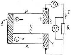
Fig. 1. Scheme of thermo e. m. f. generation in a system: metal – semiconductor: 1 – metal, 2 – semiconductor [1-12]
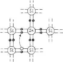
Fig. 2. Scheme of formation of “hole” [1-12]
As a result of theoretical consideration in this work, it is shown that it is possible to increase significantly efficiency of the thermoelectric generator working in a system: metal – impurity semiconductor. The necessary positive effect is reached as a result of accounting of a bulk thermo gradient effect on emergence polarized e. m. f.
Theoretical solution
From the beginning we will consider the theoretical parties of a new approach to the solution of an issue of efficiency increase of such thermo elements in terms of physics. Let elements 2 and 4 in Fig. 3 will be big, massive and bulk and they will be spatially divided. This situation is presented in Fig. 3. In terms of physics this situation will be a model of the molecules motion in two big vessels connected themselves by the reported channel, a vessel. The situation is shown in Fig. 4.
Let’s describe this process in terms of molecules kinetic theory of gases. Thus it turns out, that the first plates (2) have higher level of temperature than the second plates (4). All electrons in plate 2 will have some total kinetic energy as a result of the thermal movement
*-«F-=?-, (1)
where mv Срд _ 3^
N 1 – is quantity of free electrons in a conductivity zone. Metal plates keep in a condition of heating, δT=const all the time. It occurs as a result T 1 > T 2.
All electrons in a plate 4 will have some total kinetic energy as a result of the thermal movement
Ek = ^ = N^,(2)
where mvср^3 , „
"^==21<Т2'
N 2 – total number of electrons in a plate 4 in a vessel 3. Which belong to a zone of conductivity, to a free zone.
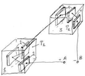
Fig. 3. Spatially divided bulk, massive thermoelements: metal -semiconductor: T 1 > T 2, 2-metal plates, 4 – semiconductors, 1 and 3 – vessels
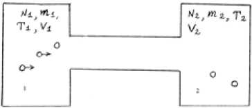
Fig. 4. The model of diffusive movement of free electrons on the basis of the scheme of communicating vessels
Some of these electrons cannot be in the zone of conductivity of plate 4. They can get deep into it, down a ladder and to take vacant positions of the free holes which are in a valency zone. You see Fig. 5-8. It occurs because of the reason that T 1 > T 2.
According to physics of process, any system aspires to an equilibrium state. In this case, it follows from the principle of thermodynamic balance of a system that
E ^ = E i< . (3)
As a result, the plate 2 will accept an additional positive charge
Q 1 - Д^ • e, (4)
where e = 1.621 ∙ 10–31 Q – electron charge, Δ N = ( N 1 – N 2) – quantity of the electrons which in addition passed into volume 3 (2) of volume 2 (1) in Fig. 3, 4. It is the quantity of electrons which counterbalances a difference of average kinetic energy of electrons in volumes 1 and 2. Respectively the plate 4 will be loaded negatively.
Approximately the following results turn out
δq = 8000 Q from 1 cm3 of coper, (5)
δU = 9.0605794 ∙ 10–3 V.
As for physics, it is known that the charge 1St = 1.054822·10-5 Q is defined by the size, as F force = 1 N at distance of 1 m. It is to compare.
Formulas (4), (5) show high value for a charge of the arisen polarization. It resulted from the temperature gradient. Let’s consider that for some unaccounted reasons of loss it will make 60%.
And then δq=3500 Q from 1 cm3 of copper. And even it will represent a high rate. All calculations are carried out at the difference of temperatures Δ t = 70 °С. It shows a huge potential stock of energy which can be received from bulk thermogradient effect.
As these data belong to 1 cm3 of initial materials (copper and semiconductor from a silicon plate), it follows that large volume of plates will be a basis of emergence of a significant polarization of charges on two different plates which are in two different vessels. Let’s explain it. When volume V that is rather big, then there will also be rather big N 1 and N 2 values. As a result, the general total average meanings of kinetic energies E 1 и E 2 will be sufficient. From this rather high level of value of the polarized charge δq follows, you watch formulas (1) – (3).
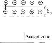
In Fig. 5-7 levels of excitation of electrons in semiconductor, arrangements of the acceptor and donor levels in a forbidden band from different impurity elements are shown [1-12].
According to Fig. 7, the implementing of a large quantity of other impurity elements in semiconductor is possible. There is a chance to achieve that between a conduction band and a valence band the whole “ladder number” of energy bands which is schematically shown in Fig. 8 is formed. These additional ladder levels of impurity atoms are necessary to facilitate transitions (jumps) of electrons in direction 1. Direction 1 shows transition of electrons from copper 2 plate to semiconductor 4 plate in Fig. 3. It is the so-called “return transition” arising as a result T 1 > T 2. That is there will be a bulk thermo gradient effect, see also Fig. 4 and formulas (1) – (5). Ladder levels (steps) will facilitate implementation of this transition in direction 1, from top to bottom. Whereas in lack of a bulk thermo gradient effect, transitions of electrons in normal, classical understanding always happens in direction 2, shown in Fig. 5 and 8.
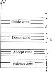
Fig. 5. Schemes of levels of excitation and direction of transition electrons in semiconductor [1-12]
Guide zone
De)nor zone
f J ®eee
Valence zone
Fig. 6. Layout and polarization of levels acceptors and donors [1-12]
Guide zone ;
[Li0,033^ Oo^ д^^ 56^0,035
Donor zone
- S QiS
_ г_ M^o^ss _
1-------- Zn.0,55 ---Гео,55?-1Г--Аи№-
_ Accept zone _ 1+ Cvto,4g
_ 2^2 fe o,4o?
In. 0Д6 Au. 0 35
- A^ QOS? i- 3 ±+
- CetQOSS Cno,24
Valence zone
Fig. 7. Arrangements of power levels impurity in Si in the forbidden zone [1-12]
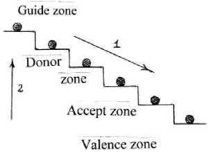
Fig. 8. Ladder structure of power levels impurity atoms in the transitional (forbidden) zone
The situation can be compared to work on drag and drop of bricks by group of working builders. When they got up in a long chain and just hand over bricks nearby to the standing person. And thus, it is possible to drag at the minimum power expenses bricks from first floor of the building site to upper floors. It makes the minimum work against gravitation forces. For example, each builder can run separately from the first floor to an upper on (on a ladder) and drag at the same time only one brick. In this case the maximum work, not useful will be spent. It will not be an effective algorithm. In our case, when electrons pass in excess quantity from a copper plate into a semiconductor plate – the thermo gradient effect makes work against forces of Coulomb pushing away the negatively charged electrons from the zone of semiconductor plates 4 in Fig. 3. or from zone 2 in Fig. 4. A conduction band electrons will pass into a valency zone (to jump) not in one step (at once in a single step), and gradually many small jumps down a step, see Fig. 8. A set of different impurity atoms will provide existence (emergence) of these steps. Their energy levels almost evenly fill all width of a forbidden band.
Thus, theoretically it is possible to prove transition in direction 1 in Fig. 5 and 8 in terms of physics. However, in our opinion, the fact that it is necessary to provide rather uniform distribution on the volume of the semiconductor of the impurity elements Na ≈ Nd ~ 1019 ÷ 1020 in 1 cm3 has certain difficulties. The greatest possible concentration of atoms in 1 cm3 is limited to number 1022.
See Fig. 2. It is necessary to be careful of process of an eutectic [18], when separate atoms and molecules of impurity substance integrate and form small volume clusters. Therefore, it is not possible to receive uniform distribution on the volume of a strange impurity as a result of a simple hashing (and further cooling) of two liquid fusions.
To receive the uniform of volume, a distribution of impurity substance in an initial crystal is used. The method of an ion of a plasma sputtering in a vacuum the is most suitable. At an electrode cathode there have to be all impurity elements and together with them the elements of the main crystal. It is Si silicon. Then, at anode deposition they will intensively mix up and form rather evenly distributed (mixed) structure. And next, it is possible to hope that each impurity atom will be surrounded on average about 100 (and more) with atoms of the main crystal of silicon. In this case, it is possible that theoretically proved "ladder structure" for transmission of energy "on top → bottom" will work effectively.
It is possible to consider other alternative option. It is sedimentation on a crystal from a steam gas phase [9-18].
The method of removal (transfer) of heat energy offered by us for creation thermo e. m. f. between large volumes of materials. It has advantages in comparison, for example, with optical polarization of charges which is used in solar power. The point is that a priori the physical nature is created in such a way that quanta of solar energy of E = h V are a little effective for removal of electrons from metals. It is about the visible light range of solar energy. Therefore, the efficiency of solar panels will be always low. It is put in principle. In comparison to it, transferring of heat energy will be more effective. The thermal waves essence is a wave of phonons. In other words, the heat transition is a process which well is controlled. Heat energy is easily transmitted from some macro volumes to others.
The equations for density of heat and mass fluxes
q = -Agrad(t), j = -pDgrad(m) (6)
allow to receive of the equation of heat and mass transition in a differential form in a final type [19]
= AV 2 t , = D^2m.
Эт дт
However, it (6) does not explain the physical reason of that in any way. Why do these heat and mass fluxes arise [20]?
In the divided big macroscopic volumes average kinetic and heat energy of all particles should be aligned. And only this physical principle (law) explains emergence of flows (6).
Due to successful implementation of the thermo battery of this new type both wind and solar energy will be used. It is known that wind power generators become bulky. The design is technically and schematically difficult. A small turn of the blade at the exit, nevertheless, requires a stable level of 220 V with a frequency of 50 Hz. Similar situation is with solar panels. It is required a stable level ∓12 or ∓24 V at different intensity of a flow of beam energy at the exit.
As interface (sharing) to a wind power generator and to a solar power unit, the new thermo power generator is offered by us. The work of the first generator (the construction and the function level) becomes considerably simpler. Namely: solar installation and the wind electric generator can work in any (simplified) mode. Even very weak, high smoothing and stabilization of their parameters at any level will not be required. It will be enough if it can heat some volume of liquid to temperature of 80÷90 °С. Is it is a progressive technological jump? During the soviet time there was a slogan:
communism is the soviet power plus electrification of the whole country. Let’s discard the first, political part of this slogan is aside. Let’s consider only the second part. According to it, if we are technologists, engineers and scientists of the whole world we will be able to provide all submultiple corners of our planet with a cheap and available type of electrical energy. Then all people will be able to raise the level of the life and welfare. Is it so?
Conclusion
-
1. The theoretical basis has been developed and the idea to practical production and testing the semiconductor electric generator (thermobattery) of a new type acting on the basis of a metal – semiconductor system has been offered. It is shown that the thermobattery will work on the basis of the use of a bulk thermogradient effect. Such effect allows to gain a sufficient level of generated power from one unit of the whole volume of a semiconductor material.
-
2. When using the semiconductor thermobattery together with solar and wind electric generators it is possible to simplify significantly constructional and technological features of these installations.
Discussion
-
1. We invite all different financial structures, owners of private, public or other capital to provide financial support for this project.
-
2. We invite scientists and specialists from all countries to work together. In case of successful realization you will become not only our assistants, but also co-authors and co-performers of our works, patents and copyright certificates. Young researchers can expect to carry out their PhD projects as part of these studies.
-
3. It is necessary to buy and catch new plants for vacuum ion plasma deposition of metals, to carry out electric discharge arc process in discharged medium.
-
4. There are some necessary things: absolutely new (at smaller dimensions) installations for cultivation of semiconductor crystals of high purity.
-
5. We need computer systems, computers for calculation and modeling of difficult physical and chemical and technological processes.
-
6. The command structure will need young perspective physicists, solid-state materials technologists, specialists of IT, programmers and other specialists.
-
7. Thank you for attention.
References About the possibility of the bulk thermo gradient effect use for the creation of the effective thermobattery
- Zherebtsov I.P. Electronics bases. L., Energoatomizdat, 1989. 352 p. (in Russian).
- Stepanenko I.P. Bases of the theory of transistors and transistorized circuits. M., Energy, 1973. 608 p. (in Russian).
- Bonch-Bruyevich of V.L. Fizik of semiconductors. M.: Science, 1990. 685 p. (in Russian).
- Ioffe A.F. Physics of semiconductors. M.-L., Academia Science, 1957. 486 p. (in Russian).
- Smith R. Semiconductors. M., World, 1982. 558 p. (in Russian).
- Stilbans L.S. Fizika of semiconductors. M.: Soviet radio, 1967. 443 p. (in Russian).
- Zeeger K. Physics of semiconductors. M., World, 1977. 615 p. (in Russian).
- Kireev P.S. Physics of semiconductors. M., The higher school, 1975. 584 p. (in Russian).
- Oreshkin P.T. Physics of semiconductors and dielectrics. M., The higher school, 1977. 448 p. (in Russian).
- Fistul V.I. Introduction to physics of semiconductors. M., The higher school, 1975. 295 p. (in Russian).
- Gavrilov R.A., Skvortsov A.M. Fundamentals of physics of semiconductors. M., mashinenbuild, 1966. 286 p. (in Russian).
- Nemenov A.A., Sominsky M.S. Fundamentals of physics and equipment of semiconductors. L., Science, 1974. 394 p. (in Russian).
- Nashelsky A.Ya. Technology of semi-conductor materials. M., Metallurgy, 1987. 335 p. (in Russian).
- Fistul V.I. Strongly doped semiconductors. M., Science, 1967. 396 p. (in Russian).
- Tsidilkovsky I.M. Electrons and holes in semiconductors. M., Science, 1972. 640 p. (in Russian).
- Sheckley V. Theory of electronic semiconductors. M., Publishing house Foreign literature, 1953. 703 p. (in Russian).
- Lebedev A.I. Physics of semiconductor devices. M., Fizmatlit, 2008. 488 p. (in Russian).
- Gorelik S.S., Dashevsky M.Ya. Materials science of semiconductors and metallurgical science. M., Metallurgy, 1973. 496 p. (in Russian).
- Isachenko V.P., Osipova V.A., Sukomel A.S. Heat transfer. M., Energy, 1975. 488 p. (in Russian).
- Zhakatayev T.A. Nonlinear models of hydrodynamics, warm, mass of exchange and burning in problems of diagnostics and control of technological processes in metallurgy. The thesis for a degree of the Doctor of Engineering. 05.16.08 Theory of metallurgical processes. Chemical and metallurgical institute of Zh. Abishev, Karaganda, 2010. 304 p. (in Russian).
