All-Optical Parity Circuits Using Nonlinear Directional Coupler

Author: L. A.Bakhtiar, E. Yaghoubi, A. Adami, S. M. Hamidi, M. Hosseinzadeh
Journal: International Journal of Modern Education and Computer Science (IJMECS) @ijmecs
Article in issue: 5 vol.5, 2013.
Free access
Since in the previous existing optical designs, the electronic-optic-electronic conversion has not been completely eliminated. Construction of the optical circuits with nonlinear waveguides can overcome this drawback. We have developed a nonlinear directional coupler theory to describe novel all-optical parity circuits. By using three channels, appropriate adjusting of the refractive indices, and selecting the correct length for coupling event, even/odd parity circuits can be obtained. The operation of these circuits is simulated with the aid of RSoft CAD-Layout (BeamPROP) simulator. Towards the end of the work, we compared the speed of our proposed novel circuit with the existing optical designs and also electronic structure of which we have a better result.
Optical computing, Parity circuit, Network security, nonlinear behaviour, Coupled mode theory
Short address: https://sciup.org/15014551
IDR: 15014551
Text of the scientific article All-Optical Parity Circuits Using Nonlinear Directional Coupler
Published Online June 2013 in MECS DOI: 10.5815/ijmecs.2013.05.08
Computers have enhanced the quality of human life, and also made it easier and more convenient. Most of the researchers’ efforts are focused on increasing the speed of computation and communication. The target of this improvement has resulted in the development of the Very Large Scale Integration (VLSI) technology with smaller device dimensions and greater complexity. Although VLSI technology can respond to our demands to reach more speed and better performance, it is approaching some fundamental limits in the sub-micron miniaturization process. As Moore's law the number of transistors on integrated circuits doubles approximately every two years. Increasing the number of transistors, however, introduces some unavoidable difficulties-dielectric breakdown, hot carriers, and short channel effects to name but a few.
All of these problems cause to decreasing device reliability. There are some solutions to solve these defects temporarily, but a long term solution is needed to overcome these physical problems permanently, and facilitate further improvements of computer performance for the future.
One of the proposed resolutions is substitution of electric current with optical beam. In other words, photons travel on optical fibres or thin films instead of electrons to perform the appropriate functions. Optical circuits have several advantages over their electronic counterparts. They provide large bandwidth and low-loss transmission. They are capable of parallel processing without short circuits or electromagnetic interference. These circuits are lightweight, compact, and more favourite because of much more stored information than corresponding electronic devices. Amongst these benefits, the speed of light impressed scientists to emphasize on replacing electric current by optical beam.
To realize the high speed of a hypothetical optical computer suppose an optical chip consists of 100
million gates, and each gate has one nanosecond switching time. This system can perform more than 1017 bit operations per second. This value compared with gigabits (109) or terabits (1012) per second rates of electronic device, shows the significant raise in computation speed. In other words, a computation that might require one hundred thousand hours (more than 11 years) of a conventional computer could require less than one hour by an optical one.
All-optical signal processing is expected to have many applications in the field of communication and computation due to its capability of handling large bandwidth signals and large information flows [1]. Elimination of optic-electronic and electronic-optic (o-e-o) conversion leads to reaching high-speed, and high-capacity functional devices in all-optical domain. Because of that, this field receiving more and more attention in recent years for applications such as addressing, switching, header recognition, data encoding, and encryption [2]. These applications are also used in network communication. In network transportation, either electrical or optical transfer, security is one of the most important issues. There are many techniques have been proposed to reach safe communication which many researchers make efforts to implement these techniques in an all-optical manner. One of the common methods is using parity bits in data packets. Typically, a parity bit is attached to a binary word before transmission of the data so that the receiver has the ability to verify the integrity of the delivered digital data [3]. When a binary digit contains an even number of ‘0’ or ‘1’, we can say that the number has an even parity. Similarly, a binary digit having an odd number of ‘0’ or ‘1’ achieves odd parity [4].
For implementing this technique, two additional circuits are needed one of them is a parity generator which generates parity bits located in sender station, and the other one is a parity checker that checks produced parity bits and detect the errors, if exist. This circuit used at the side of the receiver.
In electronic domain, these circuits fabricated with cascaded XOR gates. Fig. 1 reveals the structure of even parity generator. In the optical field there are some literatures which have been reported all-optical parity circuits. In [3] the parity circuit contains two semiconductor amplifiers (SOA) based all-optical switching gates (TOAD [5]), one for regeneration/XOR, and one for wavelength conversion, and so two different wavelengths are used to distinguish clock and data pulses. Because the all optical gates themselves have latency larger than that required for single bit delay times, therefore, in this design a bit differential method employed. It means that the binary word to be checked is input several times into all optical XOR gates.
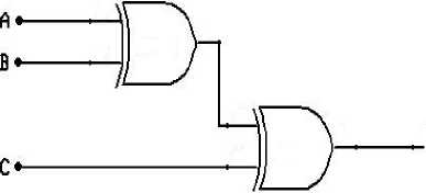
Figure 1. Three inputs even parity generator
In [4], by cascaded XOR gates all-optical parity circuits have been constructed. This scheme has been proposed with applications of optical non-linear materials. In this structure to maintain the coherence all lights must be emerged from a single light source, and also they should be in the same wavelength. The operation of this circuit largely depends on intensity of the optical beams. In [6] basic element of the circuit is a single Mach-Zehnder interferometer which is set to act as an XOR gate. The invention of this scheme is eliminating the need for the additional wavelength converter which was essential in previous all optical parity circuits by use of MZI interferometer. Finally, in [7] six semiconductor optical amplifiers (SOAs) are incorporated to perform the function of all-optical 4-bit parity checker. The cross gain modulation (XGM) effect is the basis of parity circuits in this report. The XGM effect can be used for broadband telecommunication application in the future.
In this paper, we utilize the property of optical nonlinear material like [4], but instead of cascaded XOR blocks, all-optical parity circuits have been created by using coupled mode theory.
The rest of the paper is organized as follows: Section II discusses the theoretical background. Afterwards, the details of operation principles with simulation results are presented in Section III. Comparisons between our schemes with former optical methods, and also with design in electronic domain are reported in Section IV. In Section V the paper is concluded with highlights of an open issue.
-
II. Theoretical Background
-
A. Coupled Mode Theory
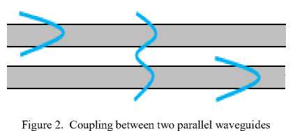
If two waveguides are sufficiently close such that their fields overlap, light can be coupled from one into the other. Optical power can be transferred between the waveguides, an effect that can be used to make optical couplers and switches [8]. Fig. 2 illustrates coupled theory.
In a Kerr-type material the refractive index, n, is described by the Kerr law, n = n0 + n2I, where n0 is the linear refractive index, n 2 is the third-order nonlinear coefficient, and I is the field intensity.
This theory can be expanded to more than two waveguides. The coupled-mode equations for a three-waveguide system are described as follows:
The amplitudes of waves derived from these differential equations:
|
do.-^ dz |
=- i^2r ехр( ∆ Pz ) a2 ( Z ) |
(1) |
|
dd2 dz |
=- jki2 ехр(- j ∆ Pz ) aT ( Z ) |
(2) |
A1(z)= -jk1A2(z)ejApiZ(6)
A2(z)= -jk1A1 (z)e-jApiZ -jk3A3 (z)e-jA₽3z(7)
A3(z)= -jk3A2(z)ejA₽3z(8)
where
In (1), (2) Δβ is the phase mismatch per unit length and k 21 , k 12 are coupling coefficients (3,4).
1k2 /-a+d k21 = (n 2 -n ) u1 (y)u2 (y) dy (3)
k12 = (n 21
k 1 га
-n2) u2 (y)u1(y)dy
β2d-a-d
A power transfer ratio is expressed as a P2/P1, which becomes:
й= 1+ ∆ ?)Т ⁄
Where P 1 and P 2 are power at the end of the waveguides, and L0 is coupling length. This term decreases as ΔβL0 increases like shown in the Fig. 3.
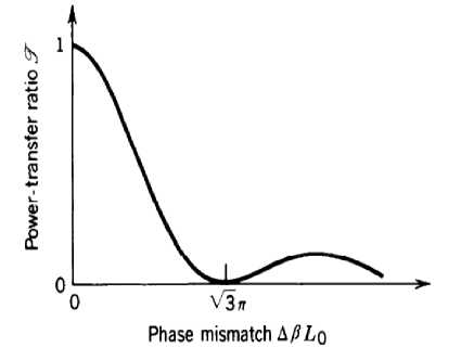
Figure 3. Power transfer ratio vs. Phase mismatch
Δβ 1 = β 1 – β 2 (9)
Δβ 3 = β 3 – β 2 (10)
And for A1(z), A2(z) and A3(z) we use the substitutions :
-
B. Linear and Nonlinear Behaviour:
Nonlinear behaviour is the response of nonlinear material to electromagnetic waves cause to changing its characteristics. The refractive index is the feature which is manipulated by the entered inputs, and the amount of changing depends on the power of applied inputs. When the light hits the molecules of the nonlinear material, the emitted light with the same energy as the input light exits if the input is weak, and thus we obtain the same waves. However, under high intensity of light, the photons can be excited to higher energy level, and emitted light with higher energy than the input light energy. This extra energy can cause to changing the refractive index of the material. By this alteration, according to coupled mode theory, the input light can propagate through other waveguides in the vicinity of the input channel. On the other hand, linear materials have a fixed refractive index, and does not effect by the intensive light. Fig. 4 shows the behaviour of nonlinear materials encounter two different inputs light.
Input tight photon energy
Emitted light photon energy
Input light photon energy
Input tight photon energy
Emittedtight photon energy
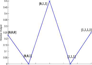
The generating circuit has three inputs {x, x, x} and each input can be ‘0’ or ‘1’, totally they have four states (Table I). In the first state {0, 0, 0}, when all inputs are zero (there is no light in port A) the output should be zero because the input contains even number of ‘1’.
TABLE I. Logical Function of Even Parity Circuit
|
State |
Output |
|
{0,0,0} |
0 |
|
{0,0,1} |
1 |
|
{0,1,1} |
0 |
|
{1,1,1} |
1 |
Figure 4. Nonlinear material behaviour: (a) Low intensity input (b)
High intensity input
III. Design And Simulation Results
In {0, 0, 1} only one input is logical one, so the number of ‘1’ in data packet becomes odd. The power of input cannot change the refractive index significantly; therefore most of power appears at the end of A port as shown in Fig. 6.
-
A. Even Parity Circuit
The proposed structure for an all-optical even-parity circuit is depicted in Fig. 5. This circuit comprises of three waveguides named as port A, B and C. Port A is used for applying inputs and receiving the output. We use PTS (n0 = 1.66 and n2=2 ×10⁻⁴ μm2/W) for this waveguide, and just this port has nonlinear behaviour [10]. Port B and C have linear behaviour, and their refractive indices are fixed at 1.6619 and 1.665, respectively. In fact, the refractive index of linear mediums set to this value by the aid of equivalent layers theory [11]. In this scheme 4 watt/um power considered logical one, and the tapered MMI-based combiner is used for combining the inputs into one output. In this combiner by introducing input light from a single-mode access waveguide, several modes are excited in the MMI section. However, the number of the excited modes decreases during propagation in the combiner due to the tapered structure, and there is only a single mode at the output [12]. The proposed structure is practical for both generating and checking parity bit.
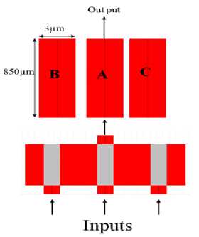
Figure 5. Even-parity circuit
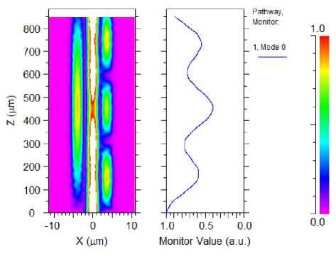
Figure 6. Normalized output power in second state {0,0,1}
In {0, 1, 1} two inputs are logical one, it means that the beam with 8 watt/um in power is launched to A port. This input can provide enough power to increase the refractive index of A channel to become equal with refractive index of B port. In this situation, most of power transferred into B port, and cause to having zero output. Finally, in the last state {1, 1, 1}, the power of inputs (12 watt/um) leads to increasing refractive index of input port. In this case, refractive indices become n C >n A >n B , thus according to coupled-mode theory the power remains in channel A, and output becomes logical one. Fig. 7 and Fig. 8 show these states.
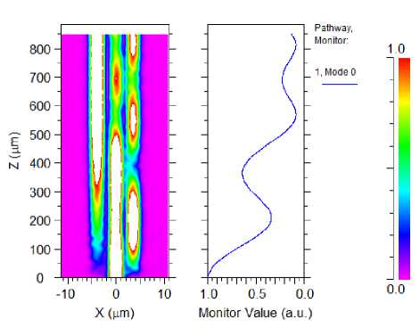
Figure 7. Normalized output power in third state {0,1,1}
In this scheme we consider one watt/um tolerance for the output. It means that if the output power is in the range of 0 ~ 1 watt/um assumed as logical zero, and if it’s between 3.5~4.5 watt/um considered as logical one. We have to note that the output power has been normalized, and so in the Pathway Monitor diagram the value of 0 ~ 1 represents the whole applied power. For example, in Fig. 8 the output is 0.35 of total power (12 watt/um) which equals to 4.2 watt/um, then it can be realized as logical one.
{1,1,1,1}, in this case the number of logical one in the inputs are even, and if there is no error in data, we would expect to have zero output as shown in above. In other states if no error exists, the value of the output is similar to the output of generator circuit. It is necessary to note that in this circuit the MMI 4×1 is utilized for power combining.
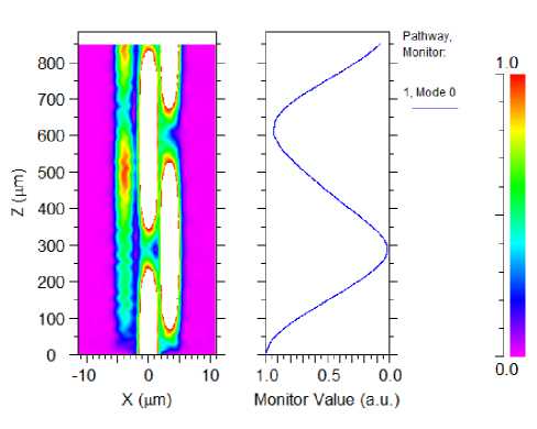
Figure 9. Normalized output power of even parity checker in state
{1,1,1,1}
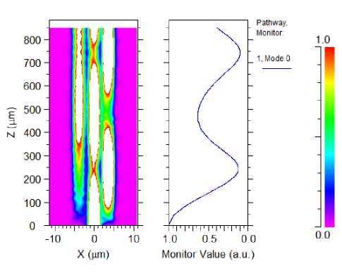
Figure 8. Normalized output power in fourth state {1,1,1}
The parity checker circuit is located at the receiver’s side to check the correctness of the parity bit. When it receives a packet of data, counts the number of '1' in it. If the result is even, it means the data delivered correctly, otherwise it's erroneous. In this case, some network's algorithms correct this error, while the others send a request to the sender for transmitting the data again. Its structure is the same as parity generator. This circuit has four inputs (3inputs and parity bit), and contains all states of generator circuit. It has an additional state
Our proposed structure has the capability of cascading because for all states the output is in a tolerable range.
-
B. Odd Parity Circuit
The odd parity circuit performs the inverse operation of even parity. Table II shows the logical function of this circuit.
TABLE II. Logical Function of Odd Parity Circuit
|
State |
Output |
|
{0,0,0} |
1 |
|
{0,0,1} |
0 |
|
{0,1,1} |
1 |
|
{1,1,1} |
0 |
The structure of odd parity is similar to former circuit, but the waveguides have different refractive indices. The refractive indices of port A and B are 1.66 and nC is 1.6608. Port A is an input port, C port is the output channel, and 3 watt/um power considered as a logical one.
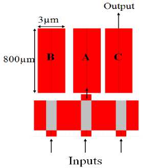
Figure 10. Odd parity circuit
A signal beam with 3 watt/um in power is always launched into B port to provide an output when the circuit is in state {0, 0, 0} (the input is zero logic).
We simulated this structure for all states. Fig. 11
shows the result of simulation in form of the diagram which determined the output power in each state. In the first state {0, 0, 0}, the number of logical one in the data is even, so the output must be one. In this state the extra input which is continually launched to the B port can provide the output. In the second state {0, 0, 1}, only one input is active, and there is odd number of logical one in the data packet. Although the light with 3watt/um in power transmitted to the input channel, this amount of power cannot change the refractive index of A port sufficiently. Thus, there is no light emerges at the output. In the case of {0, 1, 1}, two inputs are high (1), and one input is low (0). According to the truth table of odd parity, logical one is expected at the end of C channel. As mentioned before, the power is normalized, and vertical axis indicates the output power than whole input power. In the above graph, for the light with 6 watt/um in power, the 3 watt/um beam (0.5*6=3) will exit from C channel. Finally, in the last state {1, 1, 1}, all three inputs are high, and there is no light propagate through the C port. All four states explained above are related to the odd parity generator. In Odd parity checker as shown in Fig. 11 four inputs applied to the input port, and if they are errorless the output should be logical one, it means the output power is 0.25 of total power (12 watt/um) which equals to logical one. In this case similar to even parity checkers, the MMI 4×1 is used as a power combiner. This scheme doesn’t have cascading capability because in state {0, 0, 0} the power is less than logical one, and it should be amplified. We propose to apply Erbium-Doped Waveguide Amplifier at the end of channel C to compensate the power loss in this case
-
[13] . Erbium-Doped Waveguide Amplifier (EDWA), has demonstrated high gain, low noise, and also used in long distance fibre communication links.
P
Figure 11. Normalized output power vs. input power
-
IV. Comparison
-
A. Novel Designs versus Other Optical Methods
The main advantage of the proposed scheme is constructing the whole circuit with only three waveguides, while in previous designs optical logic gates used as basic elements, then by cascading them the function would be implemented. This advantage causes to reducing the size of logic circuits.
Moreover, using SOAs for designing the circuits besides input signals, they need an extra signal which is called pump input. Whereas reported scheme needs an extra signal only for odd parity. In addition, in the structure of SOAs electronic signals play a key role, and requirement of electrons does not eliminate totally. However, the proposed circuits do not need any electrical current in any states.
The main drawback of proposed circuits is deficiency of power just in the first state in odd parity which should be amplified. Comparison between novel designs and former schemes are summarized in Table III.
-
B. Optical Scheme versus Electronic Scheme
As mentioned before, one of the most advantages of using light is achieving the highest speed in computation and communication.
TABLE III. Comparison of Novel Design and Other Reported Methods
|
Scheme |
Simulator |
Experimental Setup |
Type of Circuit |
Element |
Number of Elements |
Extra Signal |
|
Proposed |
RSoft |
X |
Generator & checker |
Linear & nonlinear waveguide |
3 waveguides |
Only for Odd Parity |
|
Ref 3 |
X |
V |
Checker |
TOAD |
2 TOAD |
Both even & odd Parity |
|
Ref 4 |
X |
X |
Generator & checker |
Nonlinear material |
5 Nonlinear Material |
Both even & odd Parity |
|
Ref 6 |
X |
V |
Checker |
MZI |
1 MZI |
Both even & odd circuit |
|
Ref 7 |
MATLAB |
X |
Checker |
SOA |
6 SOA |
Both even & odd Parity |
In this section, we compare two schemes of parity circuits one of them is electronic structure which is constructed with logical gates, and the other one is proposed designs in this paper. Comparing the speed of these schemes will prove our claim.
In the electronic domain, the even parity function is constructed with two XOR gates, and odd parity with two cascaded XOR gates followed by a NOT gate. We suppose that these logical gates are fabricated with fastest silicon transistor. The switching speed of this transistor is about 10 picoseconds [14]. In CMOS technology NOT gate constructed with two transistors, one NMOS and one PMOS. XOR gate has eight silicon transistors, four NMOS for pull down networks and four PMOS in pull up network. For delay calculation of these logic gates, we evaluate worse-case path in pull down network. Therefore, the delay of NOT and XOR gate are 10 and 20 picoseconds, respectively. In Table IV the circuit diagrams of XOR/NOT and even/odd parity function in CMOS technology, and their switching speed are demonstrated.
The switching speed (Group Delay) of the proposed design is calculated with the following equation:
Group Delay=

Group delay is defined as the rate of change of transmission phase angle with respect to frequency. Group delay can be construed as a measurement of how long it takes a signal to traverse a waveguide, or its transit time. It is a proportional to the length of the waveguide, and usually a weak function of frequency. In considering group delay, in free space all electromagnetic signals travel at the speed of light. In above equation 'L' is the waveguide length, 'C' is the light speed (29.979cm/ns), 'a' is the width of waveguides (cm), and 'f' is the frequency of the input light which is equal to 'c/λ' (λ=1.55µm). Therefore, the delay of even parity function in optical domain is 2.9 Picoseconds, and the speed of odd parity circuit becomes 2.7 Picoseconds. The Table IV indicates the value of switching speed (delay) of parity circuits for both electronic and optical designs.
|
Electronic/ Optic Scheme |
Switching Speed |
|
|
XOR Gate |
J T VDD А ^L JH 5 A —<|Г J|>— S л нг JH• A fl —IL —• в |
20 Picoseconds |
|
NOT Gate |
Vdd-------- 1------ \ZSS-----------1-------- |
10 Picoseconds |
|
Even Parity Circuit(electrically) |
=•-----il_7\ |
40 Picoseconds |
|
Even Parity Circuit(optically) |
Outpu t В A C Inputs |
2.9 Picoseconds |
|
Odd Parity Circuit(electrically) |
~Fd^>- |
50 Picoseconds |
|
Odd Parity Circuit(optically) |
Outpu t ВАС Inputs |
2.7 Picoseconds |
-
V. Conclusion
As previously noted, security is one of the most important issues in network communication. Using parity bit in data packets is one of the common methods for detecting errors. This paper proposed a novel structure which is called all-optical parity circuits based on nonlinear directional coupler. Despite, these schemes are practical for generating and checking parity bit, the odd parity circuit just in one state has an imperfection, and the output needs the amplification. It is crucial to take into account that, choosing shorter or longer waveguides leads to undesirable coupling, and the correct output would not be obtained. Therefore, the length and the width of the proposed circuits are optimized. To minimize the size of the circuits, a medium with higher nonlinear index is required. The material which is used for constructing this scheme is a real one. Thus, changing this parameter to reduce the size or speed makes the medium as unreal material. As a future work we expect that metallurgy and chemistry scientists discover higher nonlinear material to make these schemes smaller, faster and efficient in terms of power consumption
References All-Optical Parity Circuits Using Nonlinear Directional Coupler
- X. Zhang, Y. Wang, J. Sun, and D. Liu, “All-optical AND gate at 10 Gbit / s based on cascaded single-port-coupled SOAs,” OSA Trends in Optics and Photonics Series, Vol. 12, 2004, pp. 124-127.
- J. Wang, J. Sun, and Q. Sun, “Proposal for All-Optical Switchable OR / XOR Logic Gates Using Sum-Frequency Generation,” Technology, Vol. 19, 2007, pp. 541-543.
- A.J. Poustie, K.J. Blow, A.E. Kelly, R.J. Manning “All-optical parity checker,” Optical Fiber Communication Conference, Vol. 1,1999, pp. 137-139.
- K.R. Chowdhury, D. De, and S. Mukhopadhyay, “Parity Checking and Generating Circuit with Nonlinear Material in All-Optical Domain,” Society, Vol. 22, 2005, pp. 1433-1435.
- A.J. Poustie, K.J. Blow, A.E. Kelly, R.J. Manning “All-optical digital processing using semiconductor optical amplifiers,” Conference of New Developments in Optical Amplifiers, Vol. 1, 1998, pp. 1-6.
- Ch. K. Yow, Y. J. Chai, K. A. Williams, R. V. Penty, I. H. White , “Enhanced performance of an all-optical parity checker using a single Mach-Zehnder interferometer,” Conference on Lasers and Electro-Optics, 2003, pp. 765-766.
- V. Priye , V. K. Srivastava, “All-optical 4-bit parity checker design,” Optica Applicata,Vol. 41, 2011, p. 157.
- B.E.A.Saleh; M.C.Teich "Fundamentals of photonics" A Wiley-Interscience publication, 1991.
- C.-min Kim and Y.-joon Im, “Switching Operations of Three-Waveguide Optical,” IEEE Journal of Selected Topics in Quantum Electronics, vol. 6, 2000, pp. 170-174.
- A. Bahrami, A. Rostami, and F. Nazari, “MZ-MMI-based all-optical switch using nonlinear coupled waveguides,” Optik - International Journal for Light and Electron Optics,Vol. 122, 2011, pp. 1787-1790.
- A. Bananej, S.M. Hamidi, W. Li, C. Li, and M.M. Tehranchi, “A flexible design for one-dimensional photonic crystals with controllable photonic bandgap width,” Optical Materials, Vol. 30, 2008, pp. 1822-1827.
- W. Zhiga, W. Zhi, K. Guiyun, and Y. Shuzhong, “Tapered Multimode Interference Combiners for Coherent Receivers,” Chinese Journal of Semiconductors, Vol. 27, 2006, pp.328-335.
- P.G. Kik and A. Polman, “Erbium doped optical waveguide amplifiers on silicon,” MRS Bulletin, Vol. 23, 1998, pp. 48-54.
- Y.M. Lin, C. Dimitrakopoulos, K.A. Jenkins, D.B. Farmer, H.Y. Chiu, A. Grill, Ph. Avouris, “100 GHz Transistors from Wafer Scale Epitaxial Graphene.” Science, Vol. 327, 2010, p. 662.
