An Analogous Computation of Different Techniques for The Digital Implementation of Inverter and NAND Logic Gates

Author: I.Hameem Shanavas, M.Brindha, V.Nallusamy
Journal: International Journal of Information Engineering and Electronic Business(IJIEEB) @ijieeb
Article in issue: 4 vol.4, 2012.
Free access
Feature size reduction in microelectronic circuits has been an important contributing factor to the dramatic increase in the processing power of computer arithmetic circuits. However, it is generally accepted that MOS based circuits cannot be reduced further in feature size due to fundamental physical restrictions. Therefore, several emerging technologies are currently being investigated. Nano devices offer greater scaling potential than MOS as well as ultra low power consumption. Nano devices display a switching behaviour that differs from traditional MOS devices. This provides new possibilities and challenges for implementing digital circuits using different techniques like CNTFET,SET, FinFET etc. In this work the design of Inverter and Nand gate using CNT, SET and FinFET has been analyzed elaborately with its own advantageous of the mentioned techniques.
CNTFET, SET, FinFET, Inverter and Nand Logic gates
Short address: https://sciup.org/15013136
IDR: 15013136
Text of the scientific article An Analogous Computation of Different Techniques for The Digital Implementation of Inverter and NAND Logic Gates
Published Online August 2012 in MECS
Steady miniaturization of transistors with each new generation of bulk CMOS technology has yielded continual improvement in the performance of digital circuits. The scaling of bulk CMOS, however, faces significant challenges in the future due to fundamental material and process technology . Primary obstacles to the scaling of bulk CMOS to sub-32nm gate lengths include short channel effects, sub-threshold leakage, gate-dielectric leakage and device-to-device variations. As nanometer process technologies have advanced, chip density and operating frequency have increased and making power consumption in battery-operated portable devices a major concern. Even for non portable devices, power consumption is important because of the increased packaging and cooling costs as well as potential reliability problems. Thus, the main design goal for VLSI (very-large-scale integration) designers is to meet performance requirements within a power budget. Therefore, power efficiency has assumed increased importance [1].
CNTFET is a novel device that is projected to outperform scaled CMOS technologies. CNTFET- based devices offer high mobility for near-ballistic transport, high carrier velocity for fast switching, as well as better electrostatic control due to the quasi onedimensional structure of carbon nanotubes. CNTFET utilizes a semiconducting carbon nanotube (CNT) channel controlled by isolated electrostatic gates. Carbon nano tubes (CNTs) are quasi one-dimensional nanostructures with unique electrical properties that make them prime candidates for applications in nano electronics. One of the most important findings in this respect is that they can be used as the channel of nanotube field-effect transistors (CNTFETs).Individual CNTFETs, and, more recently, arrays of CNTFETs with good switching characteristics have been produced. The next critical step in assessing the suitability of these devices for computer electronics involves the integration of individual CNTFETs to form logic gates. Even more exciting is the possibility of building logic gates out of a single nanotube or nanotube bundle. To build such logic circuits, one needs nanotube devices that use electrons (n-type CNTFETs) and holes (p-type) as the carriers of electricity. However, in all of the studies reported up to now, the CNTFETs made of as-prepared nanotubes invariably showed p-type characteristics, i.e., they were ON for negative gate bias. The reason for this behavior has not been resolved. N-type CNTFETs can be made by direct doping of the tube with an electropositive element such as potassium. We find that the p-type electronic character of CNTFETs is not an intrinsic property of the nanotubes. By simply annealing the CNTFETs in a vacuum, we can change their electrical character and turn CNTFETs initially behaving as p-type into fully n-type ones. In fact, we can produce in a controlled manner any intermediate situation between p- and n-type, resulting in ambipolar (i.e., electron and hole) transport. Using vacuum annealing or doping to make n-type CNTFETs, we fabricate complementary devices, i.e., p- and n-CNTFETs on the same substrate. These complementary CNTFETs are then assembled to form intermolecular logic gates. In particular, we demonstrate the fabrication of a “NOT” gate or voltage inverter. Most importantly, using spatially selective doping, we fabricate complementary CNTFETs on a single nanotube bundle, thus forming the first intramolecular logic gate. From studies , semiconducting SWNT (diameter 1.4 nm, band gap _0.6 eV) dispersed from a 1,2-dichloroethane solution on an oxidized silicon substrate pre patterned with gold electrodes.The nanotubes are side-bonded to these electrodes and the conductive backside of the Si wafer is used as the gate.[2].
Fin-type field-effect transistors (FinFETs) are promising substitutes for bulk CMOS in nano-scale circuits. It is observed that in spite of improved device characteristics, high active leakage may remain a problem for FinFET logic circuits. Leakage is found to contribute 31.3% of total power consumption in power-optimized FinFET logic circuits. Various Fin- FET logic design styles, based on independent control of FinFET gates[3].
-
II .CARBON NANOTUBES
-
2.1. CNTFET Model
Silicon-based integrated circuit technology is approaching its physical limit as the device dimensions scale to the nanometer regime[4]. In the post silicon era, carbon nanotube field effect transistor (CNTFET) is a promising candidate for future integrated circuits because of its excellent properties like near ballistic transport [5], high carrier mobility (103–104 cm2/V · s) in semiconducting carbon nanotube (CNTs) [6,7], and easy integration of high-k dielectric material resulting in better gate electrostatics. CNTs are basically hollow cylinders of rolled-up graphene sheet composed of one or more concentric layers of carbon atoms in a honeycomb lattice arrangement. Depending on the direction in which the nanotubes are rolled (chirality), they can be either metallic or semiconducting [8]. In a nanotube, low bias transport can be nearly ballistic across distances of several hundred nanometer and it is attractive for nanoelectronic applications due to its excellent electrical properties. The carbon nanotube field-effect transistor thus already achieved widespread attention as possible alternative to nanoscale MOS transistor. Due to the similar I-V characteristics of CNTFET as that of MOS devices, qualitatively most of the CMOS circuit can be implemented using CNTFET
Carbon Nano tube Field effect transistor (CNTFET) is a novel device that is projected to outperform scaled CMOS technologies. CNTFET based devices offer high mobility, high carrier velocity for fast switching as well as better electrostatic control. CNTFET utilizes a semiconducting carbon nano tube channel controlled by isolated electro static gates.CNTs are used in the channel region of the CNTFET. Different types of CNTFET have been demonstrated in the literature. There are mainly two types of CNTFET: Schottky barrier CNTFET (SB-CNTFET) and MOSFET-like CNTFET as shown Fig. 1.
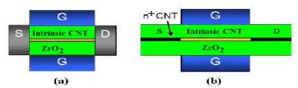
Fig.1 (a) Schottky barrier CNTFET (b) MOSFET-like CNTFET
In SB-CNTFET the channel is made of intrinsic semiconducting CNT and direct contacts of the metal with the semiconducting nanotubes are made for source and drain regions. The device works on the principle of direct tunneling through the Schottky barrier (SB) at the source-channel junction. The barrier-width is modulated by the application of gate voltage, and thus, the transconductance of the device is controlled by the gate voltage. In MOSFET-like CNTFET doped CNTs are used for the source and drain regions and channel is made of intrinsic semiconducting CNT. A tunable CNTFET with electrical doping is also proposed. It works on the principle of barrier-height modulation by the application of gate potential.
The SB-CNTFETs to design basic logic circuits. Before going into the realization of the high performance digital circuits using CNTFETs, let us discuss our simulation model. It has the compact model of double gate (DG) SB-CNTFET with ambipolar characteristics. It is a surface potential-based SPICE compatible model which is used to simulate the CNTFETs with ballistic behavior. This model is applicable to a range of CNTs with diameter between 1 to 3 nm. Figure 2 and 3 shows the digital implementations of NOT and NAND using CNT respectively.
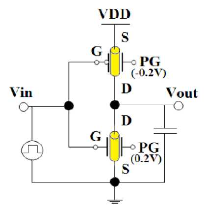
Fig. 2. CNTFET inverter schematic
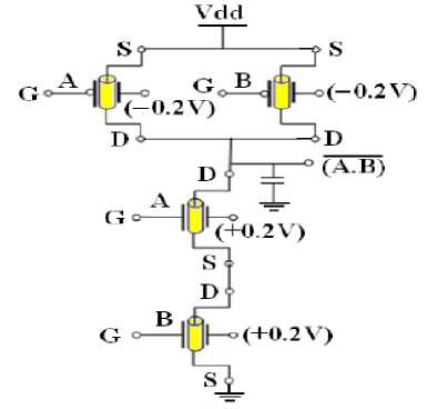
Fig. 3. Two input NAND gate using CNTFET.
-
III. SINGLE ELECTRON TRANSISTOR
The single electron transistor or SET is a new type of switching device that uses controlled electron tunneling to amplify current. An SET is made from two tunnel junctions that share a common electrode. A tunnel junction consists of two pieces of metal separated by a very thin (~1 nm) insulator. The only way for electrons in one of the metal electrodes to travel to the other electrode is to tunnel through the insulator. Since tunneling is a discrete process, the electric charge that flows through the tunnel junction flows in multiples of e, the charge of a single electron. An SET can be made by placing two tunnel junctions in series.
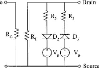
Fig.4 Simulation model of SET
The two tunnel junctions create what is known as a "Coulomb island" that electrons can only enter by tunneling through one of the insulators. This device has three terminals like a ordinary field effect transistor: the outside terminal of each tunnel junction, and a "gate" terminal which is coactively coupled to the node between the two tunnel junctions. The capacitor may seem like a third tunnel junction, but it is much thicker than the others so that no electrons can tunnel through it. The capacitor simply serves as a way of setting the electric charge on the Coulomb Island. When the gate voltage is set to zero, very little tunneling occurs through the two tunnel junctions. This opposition to tunneling is called the Coulomb blockade. However, when the gate voltage is raised to e/2Cg, which corresponds to half of the charge of an electron on the plates of the gate capacitor, the tunneling current goes up dramatically. The charge on the gate capacitor can be set to non-integral number of electron charges because charge transfer in metals is continuous. This voltage controlled current behavior makes the SET's operation much like that of a field effect transistor, but on a much smaller scale.
Usually electrons move continuously in the common transistors, but as the size of the system goes down to nanoscale (for example, the size of metal atoms can be several nm, and the size of semi-conductive particles can be several tens nm), the energy of the system is quantamized, that is, the process of charging and discharging is discontinuous. The energy for one electron to move into the system is: Ec = e**2 / 2C where C is the capacitance of this system. (1) This Ec is called Coulomb blockade energy, which is the repelling energy of the previous electron to the next electron. For a tiny system, the capacitance C is very small, thus Ec can be very high, and the electrons cannot move simultaneously, but must pass through one by one. This phenomenon is called "Coulomb blockade", and has been observed in 1980s. If two quantum dots(QD) are joined at a point and form a channel, it is possible for an electron to pass from one dot over the energy barrier and move to the other dot, this is called "tunneling phenomenon". In order to overcome the barrier (Ec), the applied voltage on the quantum dots (V/2) should be
V > e/C (2)
In order to observe Coulomb blockade and tunneling, the energy an electron assumes must be higher than the thermal scattering energy, that is e **2 /2c > KbT (3)
Where K b is the Boltzman constant. As this equation predicts, if the capacitance is low enough, that is, if the size of the QDs can be reduced to several nm, Coulomb blockade and tunneling can be observed at high (Room) temperature. The terminal currents of the SET are determined from the average charge state of the Coulomb Island of the SET. When several SET’s are connected, the charge state of the Coulomb Island of one SET is strongly affected by the charge states of neighboring islands of other SET’s. Therefore, the terminal currents of the SET in the circuit may be different from those of the isolated SET even at the same bias condition[9]. The value of the resistor is tuned by using following formula
R 1 = CR 1 + CR 2 * COS ( CF 1 * V g ) (4)
R 2 = R 3 = C * V p / (CI 2 – 2* C*V p/ R 1 ) (5)
-
3.1 SET’S Model
The single electron transistor (SET) is a new type of switching device that uses controlled electron tunnelling to amplify current. An SET is made from two tunnel junctions that share a common electrode. A tunnel junction consists of two pieces of metal separated by a very thin insulator. The electrons in one metal electrode tunnel through the insulator and travel to the other electrode. The main advantage of SET based circuits are less power consumption and high speed. This work analysed the performance of the recent possibilities for implementing the digital circuits .
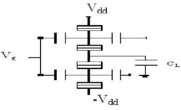
Fig. 5 Inverter Using SET
The Fig 5 shows the SET inverter. When combining two complementary biased SET transistors in a single circuit, we arrive at the SET inverter structure . The upper SET transistor behaves similar to a p-type transistor, while the lower transistor operates similar to an n-type transistor. Output switching (from 0 to 1) is accomplished by transporting electrons (typically over 100) from the output node n2 to the top supply voltage terminal Vs, or (from 1 to 0) by transporting electrons from the bottom ground terminal to the output node n2. Given that SET transistors can be biased such that they behave similar to p or n transistors, we can convert existing CMOS cell libraries to their SET equivalents.
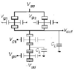
Fig.6 NAND Gate Using SET
First, the designs only operate correctly when the current though an “open” transistor consists of a large number of electrons. Given that electron tunneling is a sequential process, this is obviously a far slower process then the transport of only one electron through the same junction. Second, the “closed” transistor is not completely closed, resulting in a static current and a dramatic increase in power consumption.
Table: Comparison of CMOS and CSET
|
Device |
Speed |
power |
Number of Transistors |
|
CMOS |
250MHZ-1GHZ |
546.61 mw |
272 |
|
CSET |
10GHZ |
27.2nw |
272 |
IV . FINFET
FinFET , a double gate field effect transistor is more versatile than traditional single gate field effect transistors because it has two gates that can be controlled independently. The second gate is used to dynamically control the threshold voltage of the first gate in order to improve the performance and leakage power. FinFET logic has significant advantages over static CMOS logic and pass transistor logic in terms of power consumption and cell area. FinFET is equivalent to two MOSFETS connected in parallel. FinFET logic circuits achieve significant area and power reduction without voltage or transistor scaling.
The additional back gate of a FinFET gives circuit designers many options. The back gate can serve as a secondary gate that enhances the performances of the front (primary) gate. For example, if the front gate voltage is VDD (transistor is ON) the back gate can be biased to VDD to provide bigger current drive, which reduces transistor delay. If the front gate voltage is 0 (transistor is OFF), the back gate can be biased to 0, which raises the threshold voltage of the front gate and reduces the leakage current. Most recent FinFET circuit researches, such as FinFET SRAM, focus on utilizing the back gate to improve circuit performance. On the other hand, the back gate can also be used to reduce the number of transistors needed to implement many logic functions. For a NFinFET, the transistor turns on if either the front gate or the back gate is VDD – this is equivalent to two NMOS transistors in parallel. Recent researches, such as a 3-transistor FinFET NAND gate, utilize this property. However, we have not seen any research that utilizes this property beyond a simple logic gate such as a NAND gate. The focus of this paper is to expand the idea of using both gates of FinFET as inputs to more complicated logic circuits, and provide insight on how to design a FinFET-based circuit with independent inputs for any logic function.
TCMS is based on the observation that in an overdriven inverter, both subthreshold leakage and current drive can be controlled simultaneously[10]. We illustrate this concept using Fig. 7, where inverter (a) is a so-called high-Vdd inverter, that is, it is connected to VHdd and VH ss. Inverter (b) is a low-Vdd inverter, that is, it is connected to VLdd and VLss. The values of VHdd, VHss, and VLdd are 1.08, _0.1 and 1.0 V, respectively. VL ss is assumed to be tied to a ground. Inverter (b) is, thus, overdriven. From this point on, it is assumed that any inverter connected to VH Dd is also connected to VHss and similarly for the lower supply voltages. To illustrate the principle of TCMS, let Vin in Fig. 7 be held at the logic 0 voltage and, thus,V ¼ VHdd. Then, subthreshold leakage through inverter (b) is determined by the leakage through the p-type FinFET, while the inverter’s delay is determined, to a large extent, by the current through the n-type FinFET. According to the above equation, the Vth of the p-type FinFET is increased due to the reverse-biased voltage of 0.08 V observed at its gates, thereby reducing subthreshold leakage. The Vth of the n-type FinFET, which is operating in the strong-inversion region, is not appreciably altered. Nevertheless, it experiences a forward-biased voltage of 1.08 V, which is higher than the normal gate drive of 1.0 V at the inverter input. This leads to a somewhat higher drive current. Similarly, the application of a logic 1 voltage at the circuit input leads to a reduction in the leakage of the n-type FinFET and improvement in the drive strength of the p-type FinFET.
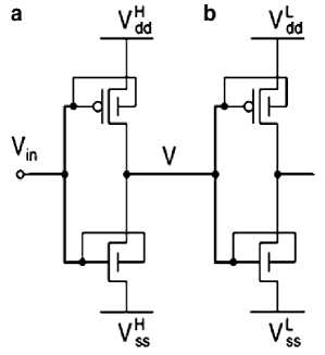
Fig.7 Inverter using FinFET
TCMS can be extended to any logic gate based on SGmode FinFET logic gates. This is explained next. Consider the two-input NAND gate shown in Fig. 8. The power supply voltages for the NAND gates are VL ddand VLss. Consider the two inputs a and b. They may be the outputs of a high-Vdd gate or a low-Vdd gate (a high-Vdd gate is connected to VH dd and VHss, and a low-Vdd gate to VLdd and VLss). During circuit synthesis, when this gate is embedded in a larger circuit, it might so happen that a is the output of a high-Vdd gate and b comes from a low-Vdd gate, or vice versa. Suppose the former is true. Thus, the FinFETs connected to input a follow the TCMS principle explainedabove. FinFETs connected to input b cannot employ the TCMS principle because there is no gate-to-source voltage difference to exploit.On the other hand, if the power supply voltages for the NAND gate are VHdd and VH ss, then the FinFETs connected to input a will not be able to take advantage of the TCMS principle. Also, input b is from the output of a low-Vdd gate and is driving ahigh-Vdd gate. This results in an increased leakage current because the p-type FinFET is forward-biased by VHdd _ VLdd. To avoid this problem, a level-convertermay be used to restore the signal to VH dd. These level-converters may be combined with a flip-flop, as in the clustered voltage scaling (CVS) technique , to minimize the power for voltage-level restoration. In an “asynchronous” approach, such as extended clustered voltage scaling (ECVS), level-converters may be inserted between logic gates connected to VL dd and VHdd . In such schemes, the power and delay overheads for the level-converters are large.
In the case of TCMS, using level-converters is not an attractive option, because power savings are obtained through the use of overdriven gates, the frequent use of which necessitates frequent level conversion. However, level conversion can be built into logic gates without requiring the use of levelconverters , through the use of a high-Vth FinFET at the inputs of high-Vdd gates that need to be driven by a low-Vdd input voltage. FinFET Vth may be controlled through a number of mechanisms. For example, there are several process-related options to statically control the Vth of a FinFET, e.g., channel doping, gate work function engineering, or asymmetrical double gates . The first step towards evaluating the utility of the TCMS principle for arbitrary logic circuits involves the design of technology libraries, consisting of high-Vdd cells, low-Vdd cells, low-Vdd cells that are being driven by high-Vdd cells, and high- Vdd cells that are being driven by low-Vdd cells. All these cells have to be characterized at both high-Vth and low-Vth. Thus, the design variables that need to be targeted are supply voltage, input gate voltage, and threshold voltage. Hence, for a two-input NAND gate of a given size, we have five design variables: supply voltage, gate input voltage for input a, gate input voltage for input b, Vth for FinFETs connected to input a, and Vth for FinFETs connected to input b. If the Vth of a p-type FinFET connected to an input is high (low), then thecorresponding n-type FinFET connected to the same input also has a high (low) Vth.
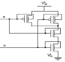
Fig.8 Nand gate using FINFET
V.CONCLUSION
In conclusion, we have discussed various logic styles for Inverter and NAND Gate. We demonstrated that the rich diversity of design styles, can be used effectively to reduce total active power consumption in digital circuits. We presented a systematic study of the area overheads and power savings with different design styles and provided a new hybrid design style that enables useful trade-offs between circuit area and power consumption.
References An Analogous Computation of Different Techniques for The Digital Implementation of Inverter and NAND Logic Gates
- Anish Muttreja, Niket Agarwal and Niraj K. Jha,,"CMOS Logic Design with Independent-gate FinFETs",IEEE Transactions,2007
- Subhajit Das, Sandip Bhattacharya, Debaprasad Das," Design of Digital Logic Circuits using Carbon Nanotube Field Effect Transistors", International Journal of Soft Computing and Engineering (IJSCE) ISSN: 2231-2307, Volume-1, Issue-6, December 2011.
- Michael C. Wang," Low Power, Area Efficient FinFET Circuit Design", Proceedings of the World Congress on Engineering and Computer Science 2009 Vol I WCECS 2009, October 20-22, 2009, San Francisco, USA
- International Technology Roadmap for Semiconductors (ITRS) reports, http://www.itrs.net/reports.html
- Hong Li, Chuan Xu, Navin Srivastava, and Kaustav Banerjee, "Carbon Nanomaterials for Next-Generation Interconnects and Passives: Physics, Status, and Prospects", IEEE Trans. Electron Devices, vol. 56, no. 9, Sep, 2009.
- Ali Javey, Jing Guo, Qian Wang, Mark Lundstrom, and Hongjie Dai, "Ballistic carbon nanotube field-effect transistor," Nature, vol. 424, pp. 654-657, 2003.
- J. Guo, A. Javey, H. Dai, and M. Lundstrom, "Performance analysis and design optimization of near ballistic carbon nanotube FETs," IEDM Tech. Digest, pp. 703-706, 2004.
- R. Saito, G. Dresselhaus, and M. S. Dresselhaus, Physical Properties of Carbon Nanotubes. London: Imperial College Press, 1998.
- K. Rathnakannan and P. Vanaja Ranjan ,"Binary Coded Decimal Arithmetic Computation using Single Electron Transistor", International Journal of Nanotechnology and Applications,ISSN 0973-631X Volume 1 Number 2 (2007) pp. 61-72
- Michael C. Wang,"Independent-Gate FinFET Circuit Design Methodology", IAENG International Journal of Computer Science, 37:1, IJCS_37_1_06
