An approximate 4-2 compressor based on spintronic devices

Author: MohammadAli Shafieabadi, Fazel Sharifi, MohammadMehdi Faghih
Journal: International Journal of Modern Education and Computer Science @ijmecs
Article in issue: 8 vol.11, 2019.
Free access
In many classes of applications, mainly in signal and image processing applications, decreasing the static power of computational circuits is a challenge. Multipliers are typically located on the critical path of such systems. A promising approach for energy-efficient design of digital systems is approximate or inexact computing. On the other hand, leakage power and limited scalability become serious obstacles that prevent the continuous miniaturization of the conventional CMOS-based logic circuits. Spin-based devices are considered as promising alternatives for CMOS technology due to their proper characteristics such as near-zero current leakage, sustainability, integrity, low standby power. In this paper a new low power approximate 4-2 compressor is presented which is implemented using spintronic devices. The proposed design is utilized in a multiplier tree for image processing applications. We have simulated and compared the proposed design with state-of-the-art designs in both quantitative and qualitative metrics. The simulation results show that the proposed design has 92% and 188% lower power consumption and PDP, respectively compared to the best state-of-the-art design.
Approximate computing, 4-2 compressor, Multiplier, spintronic technology, Low Power Design
Short address: https://sciup.org/15016871
IDR: 15016871 | DOI: 10.5815/ijmecs.2019.08.04
Text of the scientific article An approximate 4-2 compressor based on spintronic devices
Published Online August 2019 in MECS DOI: 10.5815/ijmecs.2019.08.04
Nowadays, with the rapid growth of the Internet of Things (IOT), the demand for designing high performance and low power portable devices has been increased. Among these devices, Digital signal processing (DSP) circuits are the heart of many of portable devices to perform special multimedia processing [1, 2].
Multiplication is one of the most critical operations in the DSP system [2, 3]. The multiplication process is performed in three steps. In the first step, partial products are made from multiplicand and multiplier operand. In the second step, partial products reduced to two operands by using compressors in parallel manner to remove the propagation delay. In the third step, the final result is obtained through the high-speed summation mechanism. In the above steps, the reduction phase has the most area and power consumption [4-6]. Therefore, the efficient design of compressors, as the main component in reduction phase, will increase the efficiency of multipliers.
Over the past years, many approaches have been proposed to reduce energy consumption, delays, and area in the compressor cells [5, 7]. Recently, approximate computing has been widely considered in algorithmic circuit design to overcome the power issue by exploiting the non-brittle perceptual abilities of human beings[7]. In the other words, human beings have limited vision perception ability for image and video, enabling circuits to have approximate results rather than accurate. So, utilizing inexact data in error-tolerant applications, will cause energy efficiency [8, 9]. Approximate (inexact) techniques can be used at three level of design hierarchy: software, architecture, and circuit levels. This paper presents a circuit-level technique for design and implementation of a 4-2 compressor as the main component in the multipliers structure.
Despite the efforts made by researchers to achieve more efficient circuit design, FET technology face major constraints and challenges such as high leakage power, dynamic energy consumption, gate control reduction and process variation sensitivity [10-12]. So, finding an alternative to avoid these problems has become an urgent need. Among the emerging technologies, spin-based devices are considered due to proper characteristics such as near-zero leakage current, sustainability, integrity, low standby power, etc. [7, 13]
In addition, spin-based devices are able to support nonvolatility in logic circuits to resolve the power-consuming issues. Therefore, the long data traffic between memory and logic chip is omitted causing lower energy consumption.
In this paper, a low power hybrid Spin/MOS 4-2 compressor is proposed. One of the key features of the proposed design is low complexity and simple structure due to the use of majority gates and approximate computing.
The rest of the paper is organized as follows: in section 2, a brief review of the STD (spintronic threshold device) is introduced and the majority gate is presented based on this structure. In section 3 the state of the art is reviewed. The proposed approximate 4-2 compressor structure is presented in section 4. In section 5, the simulation results and comparison with other previous results are discussed. Finally, section 6 concludes the paper.
-
II. Majority Gate based on a Spintronic Threshold Device
In this section, we describe a 3-input majority gate based on the Spintronic Threshold Device (STD). At first, we introduce the Spintronic Threshold Device (STD)[7, 14]. The STD structure consists of a domain wall motion (DWM) magnetic tape with a magnetic tunnel junction (MTJ). MTJ consists of two ferromagnetic layers (FM), that a tunneling oxide layer (MgO) is sandwiched between them [15, 16]. As shown in Fig. 1, STD consists of a thin and short (2nm×20nm×50nm) magnetic Domain Wall Stripe (DWS) connecting two fixed anti-parallel magnetic domains (Node1 and Node2). Magnetizing the DWM strip can be either antiparallel (AP) or parallel (P) by injecting a current value greater than the threshold current from its write terminals (Node1 and Node2). The anti-parallel and parallel states are equivalent to the high resistance and low resistance states respectively. The ratio of two resistances of the parallel and anti-parallel states is called the Tunneling Magneto Resistance Ratio (TMR)[17]. Based on the simulation results and experimental data available in [7, 18], the threshold current (I th ) for changing the DW magnetic state is 30 μA at 1ns. It is worth noting that the sense current (≅1 μ A) is significantly less than the DW threshold current so that the state of the MTJ is not disturbed during a read operation. The resistance states are binary, i.e. either high (corresponding to AP configuration) or low (corresponding to P configuration) and can be read employing the Spin-TD sense circuit as shown in Fig. 2).
Write Current
Reset Current
Read Current
Tunneling
Node3
L FL
W FL
Node1
Oxide FLiaxyeedr
Fixed Fixed
Contact Metal
L nws
Fig.1. Spintronic threshold device structure (STD)
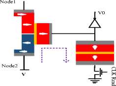
Fig.2. STD sense circuit
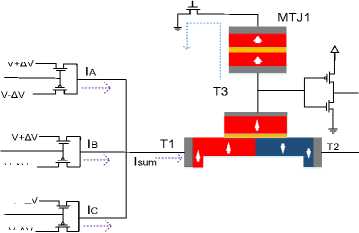
Fig. 3, shows a 3-inputs majority gate based on the STD. When two or three inputs have a value of "1", the output of the majority gate function will be equal to "1". In general, for an N-input majority function, the output will have value of "1" when more than (N-1)/2 inputs (N is an odd integer greater than 1) have value of "1". Input nodes of MAJ3 are connected via the Node1 of the STD device through a network pairs of N and P type transistors. The source and drain terminals of these transistors have V+ΔV=550mV and V-ΔV=450mV, respectively. Node2 is connected to source V=500mV in STD. With these voltages, as well as the size of the transistors, the flow in the magnetic tape is + 30μA or -30μA, which is enough to move the domain wall. If two or three inputs are "1", more than two transistors are connected to 550 mV, so the DW is shifted to the left and therefore the MTJ resistance is high (anti-parallel). Otherwise, the DW will be moved to the right and the MTJ will have a low resistance (parallel) value.
Input current
Sence current
CLK sense
Vo
V
V-ΔV
Fig.3. Three-input majority gate based on STD
V V+ΔV A
V+ΔV
B
V-ΔV
V+ΔV
c
Table 1. provides more details on the performance of the majority gate and DW position. As already mentioned, reference MTJ in STD device, has a resistance between the parallel and anti-parallel resistance. Therefore, with using the voltage division, the voltage of Node3 can be adjusted. For example, when the input pattern is "000", the DW is on the right and the resistance is low (P), and therefore the voltage of the Node3 is high and, therefore, the output voltage (Vo) is equal to "0".
Node2
Table 1. Input Current summation at Node1 and DW position and its corresponding resistance for three-input majority gate
|
Inputs ( μ A) |
Summation ( μ A) |
Final DW position |
MTJ resistance |
||
|
A |
B |
C |
Σ(A,B,C) |
||
|
0(-30) |
0(-30) |
0(-30) |
0(-90) |
Right |
Low |
|
0(-30) |
0(-30) |
1(+30) |
1(-30) |
Right |
Low |
|
0(-30) |
1(+30) |
0(-30) |
1(-30) |
Right |
Low |
|
0(-30) |
1(+30) |
1(+30) |
2(+30) |
Left |
High |
|
1(+30) |
0(-30) |
0(-30) |
1(-30) |
Right |
Low |
|
1(+30) |
0(-30) |
1(+30) |
2(+30) |
Left |
High |
|
1(+30) |
1(+30) |
0(-30) |
2(+30) |
Left |
High |
|
1(+30) |
1(+30) |
1(+30) |
3(+90) |
Left |
High |
-
III. State-of-the-arts
The details of two spin based approximate 4-2 compressor cells are described in this section. Before that, we will discuss a summary of how a 4-2 compressor works and its functionality. A 4-2 compressor is a computational block that, according to (1), reduces the five inputs x 1 , x 2 , x 3 , x 4 , and c in to three outputs sum , carry and c out.
x1+x2+x3+x4 +C(n = sum + ( carry+ cou ^) ■ (1)
Schematic of 4-2 compressor design is shown in Fig. 4
architecture. In the first design, both full adders are imprecise, while in the second design, the imprecise subblock is the second full adder. The diagram of these two imprecise compressor designs is shown in Fig. 6.
-
IV. Propused Disgn
In this section, an imprecise 4-2 compressor with low power consumption and low complexity, based on the structure described in section 2 is presented. The logical description of proposed approximate compressor is stated in (5-7). Based on these equations, the proposed scheme can be based on the three or five inputs majority gate as shown in Fig. 7.
x 1 x 2 x 3 x 4
MM
4-2 Compressor cin
Cell
carry sum
Fig.4. General schematic of a 4-2 compressor
As shown in Fig. 5, the structure of exact 4-2 compressor can be formed of two full adders that are hierarchically connected to each other. To avoid the carry propagation delay and accelerate carry value, the output carry ( c out ) should be independent of the input carry ( c in ). The logical description of an exact 4-2 compressor is described in the following equations (2-4).
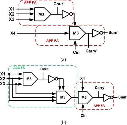
Fig.6. Schematic of presented approximate 4-2 compressor in [7](a) Design I (b) Design II
cout = x1x2 +x2x3 +x1x3 = MAJ3 ( x1,x2,x3 ) ■
sum=s Ф x ^ Ф c- ^. (3)
4 in carry = s•(cin e x4) + cin x44. (4)
where, s denotes XORing the x 1 , x 2 , and x 3 inputs.
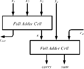
Fig.5. A 4-2 compressor composed of two full adder
In [7] two imprecise 4-2 compressors based on exact and inexact full adder according to the architecture presented in Fig. 5 are introduced. The ideas of these designs are due to the approximation of one or both of cascaded full adder in the exact 4-2 compressor
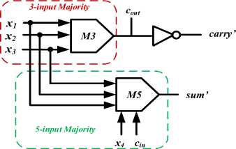
Fig.7. The proposed approximate 4-2 compressor design
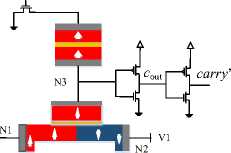
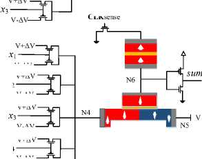
The c out of this imprecise compressor is to be similar to the exact compressor and is generated via a 3-input majority gate with x 1 , x 2 , and x 3 as inputs. In the proposed design, the output carry is obtained via inverting the output of c out . Also, the inexact sum output is generated with a 5-input majority gate which is fed with all five inputs of the compressor. Unlike the exact 4-2 compressor, the approximate sum and carry outputs are generated directly from the input signals.
cout =MAJ3 ( xi,x2,x3 ) ■
sum' = MAJ5 ( XpX2,x^,x^, c n ) .
carry' = cout .
Table 2. demonstrates the truth table of the exact and the proposed inexact 4-2 compressor. In this table, the output of C out for the proposed design is the same as the exact design. The error distance of each min-term is given in each row. The cout is error free, and the number of errors in the carry and sum output is 12 and 10 out of
-
32, respectively. With considering the fact that a number of errors overlap in the sum and carry output, the total number of suggested compressors’ errors is 12. As explained in the previous section, spin-based structures are very suitable for designing majority-based circuits. Approximate 4-2 compressor proposed by a 3-input majority gate to produce a c out and uses a 5-input majority gate to generate an estimated sum of output. According to the above descriptions, the VLSI implementation of the approximate 4-2 compressor is shown in Fig. 8.
Table 2. Truth table of the proposed imprecise 4-2 compressor design and exact 4-2 compressor
Inputs
Exact Outputs
Proposed Design
c in
x 4
x 3
x 2
x 1
c out
carry
sum
carry
sum
ED
0
0
0
0
0
0
0
0
1*
0
2
0
0
0
0
1
0
0
1
1*
0*
1
0
0
0
1
0
0
0
1
1*
0*
1
0
0
0
1
1
1
0
0
0
0
0
0
0
1
0
0
0
0
1
1*
0*
1
0
0
1
0
1
1
0
0
0
0
0
0
0
1
1
0
1
0
0
0
0
0
0
0
1
1
1
1
0
1
0
1
0
0
1
0
0
0
0
0
1
1*
0*
1
0
1
0
0
1
0
1
0
1
0
0
0
1
0
1
0
0
1
0
1
0
0
0
1
0
1
1
1
0
1
0
1
0
0
1
1
0
0
0
1
0
1
0
0
0
1
1
0
1
1
0
1
0
1
0
0
1
1
1
0
1
0
1
0
1
0
0
1
1
1
1
1
1
0
0*
1*
-1
1
0
0
0
0
0
0
1
1*
0*
1
1
0
0
0
1
0
1
0
1
0
0
1
0
0
1
0
0
1
0
1
0
0
1
0
0
1
1
1
0
1
0
1
0
1
0
1
0
0
0
1
0
1
0
0
1
0
1
0
1
1
0
1
0
1
0
1
0
1
1
0
1
0
1
0
1
0
1
0
1
1
1
1
1
0
0*
1*
-1
1
1
0
0
0
0
1
0
1
0
0
1
1
0
0
1
0
1
1
1
1
0
1
1
0
1
0
0
1
1
1
1
0
1
1
0
1
1
1
1
0
0*
1*
-1
1
1
1
0
0
0
1
1
1
1
0
1
1
1
0
1
1
1
0
0*
1*
-1
1
1
1
1
0
1
1
0
0*
1*
-1
1
1
1
1
1
1
1
1
0*
1
-2
x 1
V+ΔV

V-ΔV
V+ΔV
x 2 -------J
V-ΔV
CLK sense
V+ΔV
CLK sense
V+ΔV
V+ΔV
V-ΔV
V+ΔV
c in -------J
V-ΔV
Fig.8. Circuit implementation of the proposed design
V-ΔV
V+ΔV x 2
V-ΔV
V-ΔV
V+ΔV x 4
Table 3. Simulation results and comparison of imprecise compressor designs
Design
Power ( μW )
Delay ( ns )
PDP ( fJ )
EDP ( ns×fJ )
Device Count
Design 1 [7]
19.863
3
59.5893
178.7679
24FinFE
T+4MT J+2DW
Design 2 [7]
26.139
3
78.4197
235.2591
36FinFE
T+6MT J+3DW
Proposed Design
10.332
2
20.6658
41.3316
24FinFE
T+4MT J+2DW
For qualitative evaluation, we quantify the produced errors of the proposed 4-2 compressor as well as their related counterparts. The criteria that determine the accuracy and reliability of the compressor cells are the mean error distance (MED) and the normalized error distance (NED). MED or mean absolute error can be calculated using the error distance (ED) according to (8):
1 22N
22N i= ∑ 1 I EDi .
-
V. Simulation Result And Discussions
The evaluation of the proposed design is presented in this section, for the quantitative evaluations, the simulation was performed using Fin FET PTM technology of 16nm in Synopsys HSPICE simulator.
In the simulated environment; both CLK compute and CLK sense are equal to 1ns, which is sufficient to change the DW position and sense it (Fig. 8). The power analysis results in the proposed scheme compared to the spinbased 4-2 compressor previously presented indicate that the design is superior to the other previous designs. Simulation results indicate that the evaluation criteria of the proposed scheme are better than the previous works[7]. As shown in Table 3 , the proposed design has lower energy consumption than the previous designs[7]. Also, since the proposed compressor has a one-stage delay, so the delay is only a CLK compute (1ns) and a CLKsense (1ns), which imposes a delay of 2ns to calculate the expected result. The designs presented in [7] apply the delay of 3ns due to two calculation steps (Fig. 6). Therefore, it needs two CLK compute and a CLK sense , which totals 3ns. In terms of energy consumption (PDP), the proposed design has lower value compared to design 1 and Design 2 [7]. In term of EDP, the improvement is even higher than energy consumption.
ED i is the difference between the exact output and the approximate output for i-th input vector. NED is used to compare the approximate designs, regardless of their size. NED Can be defined according to (9) [19]:
NED=
MED
1 2 ∑ I EDi I
22N i= ∑ 1 D
.
D, represents the maximum ED value in an approximate multiplication, for investigating the impact of the proposed imprecise 4-2 compressor, an 8×8 unsigned Dadda tree multiplier is considered (Fig. 9).

Fig.9. Reduction process of 8×8 unsigned Dadda tree multiplier
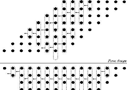
Second Stage
Table 4. , shows the results of multiplier according to the proposed design and the two previous proposed compressors[7]. The results show the proposed design has lower PDP ∗ NED than the other designs.
Table 4. Accuracy as well as its trade of with power and energy dissipation comparison for 8×8 multiplier using proposed and previous imprecise compressors
|
Design |
MED |
NED |
Power×NED |
Energy×NED |
|
Design 1[7] |
4275.22 |
0.06574 |
1.305 |
3.917 |
|
Design 2 [7] |
3268.57 |
0.05026 |
1.313 |
3.941 |
|
Proposed |
6377.65 |
0.09150 |
0.945 |
1.890 |
-
VI. Conclusion
In this paper, we proposed an approximate spin-based 4-2 compressor. The proposed design implemented based on majority gates. We have presented schema, equations and VLSI implementation of the proposed design. Synopsis HSPICE simulator is used to evaluate and show the correct functionality of the proposed circuit. The simulation results clearly show that the proposed design have lower power consumption than previous designs. For example, 47.97% reduction in power consumption can be reported for proposed design, over the previous design. Also, the proposed design has lower PDP, EDP a PDP*NED compared to the state of the art designs. In addition, the utility of the proposed spin-CMOS approximate 4-2 compressor is demonstrated in an image processing application. The result of image multiplications in terms of the PSNR values and visually, are comparable and acceptable.
References An approximate 4-2 compressor based on spintronic devices
- Gautschi, “Design of energy-efficient processing elements for near-threshold parallel computing,” 2017, ETH Zurich.
- M. Gautschi, and et al., “Near-threshold RISC-V core with DSP extensions for scalable IoT endpoint devices,” IEEE Transactions on Very Large Scale Integration (VLSI) Systems, 2017. 25(10): p. 2700-2713.
- W. Liu, S. Fan, A. Khalid, C. Rafferty, and M. O'Neill, “Optimized Schoolbook Polynomial Multiplication for Compact Lattice-Based Cryptography on FPGA,“ IEEE Transactions on Very Large Scale Integration (VLSI) Systems, 2019.
- S. Hsiao, M. Jiang, and J. Yeh, “Design of high-speed low-power 3-2 counter and 4-2 compressor for fast multipliers,” Electronics Letters, 1998. 34(4): p. 341-343.
- A. Arasteh, M. Moaiyeri, M. Taheri, K. Navi, and N. Bagherzaseh, “An energy and area efficient 4: 2 compressor based on FinFETs,” Integration, 2018. 60: p. 224-231.
- C. Chang, J. Gu , and M. Zhang, “Ultra low-voltage low-power CMOS 4-2 and 5-2 compressors for fast arithmetic circuits,” IEEE Transactions on Circuits and Systems I: Regular Papers, 2004. 51(10): p. 1985-1997.
- S. Angizi, H. Jiang, R. F.DeMara, J. Han, D. Fan, “Majority-based spin-CMOS primitives for approximate computing,” IEEE Transactions on Nanotechnology, 2018. 17(4): p. 795-806.
- D. Balobas and N. Konofaos, “Low-power high-performance CMOS 5-2 compressor with 58 transistors,” Electronics Letters, 2018. 54(5): p. 278-280.
- S. Agarwal, G. Harish, S. Balamurugan, and R. Marimuthu ,”Design of High Speed 5: 2 and 7: 2 Compressor Using Nanomagnetic Logic,” in International Symposium on VLSI Design and Test. 2018. Springer.
- P. Nejadzadeh, and M.R. Reshadinezhad, “Design of an Efficient Current Mode Full-Adder Applying Carbon Nanotube Technology,” International Journal of Modern Education and Computer Science, vol. 10, p. 43, 2018.
- F. Sharifi, and H. Thapliyal, “Energy-efficient magnetic circuits based on nanoelectronic devices,” in 2017 IEEE International Symposium on Circuits and Systems (ISCAS). 2017. IEEE.
- H. Thapliyal, F. Sharifi, and S.D. Kumar, ” Energy-efficient design of hybrid MTJ/CMOS and MTJ/nanoelectronics circuits,” IEEE Transactions on Magnetics, 2018. 54(7): p. 1-8.
- E.Raymenants , and et al, “Scaled spintronic logic device based on domain wall motion in magnetically interconnected tunnel junctions,” In 2018 IEEE International Electron Devices Meeting (IEDM) (pp. 36-4). IEEE.
- S. Angizi, Z. He, R. F.DeMara, and D. Fan, ” Composite spintronic accuracy-configurable adder for low power digital signal processing,” 18th International Symposium on Quality Electronic Design (ISQED). 2017. IEEE.
- X. Fong, and et al., ” Spin-transfer torque devices for logic and memory: Prospects and perspectives,” IEEE Transactions on Computer-Aided Design of Integrated Circuits and Systems, 2015. 35(1): p. 1-22.
- D. Zhang, and et al., “Reliability-enhanced hybrid CMOS/MTJ logic circuit architecture,” IEEE Transactions on Magnetics, 2017. 53(11): p. 1-5.
- H. Honjo, and et al., “Critical role of W insertion layer sputtering condition for reference layer on magnetic and transport properties of perpendicular-anisotropy magnetic tunnel junction,” IEEE Transactions on Magnetics, 2019.
- S. Fukami, and et al, ”20-nm magnetic domain wall motion memory with ultralow-power operation,” IEEE International Electron Devices Meeting. 2013.
- J. Liang, J. Han, and F. Lombardi, “New metrics for the reliability of approximate and probabilistic adders,” IEEE Transactions on computers, 2012. 62(9): p. 1760-1771.
