An optimized approach towards reversible adder/subtractor design on QCA

Author: Snigdha Singh, Abhinay Choudhary, Manoj Kumar Jain
Journal: International Journal of Modern Education and Computer Science @ijmecs
Article in issue: 10 vol.11, 2019.
Free access
In the present era of miniaturization, higher power dissipation in form of heat has become a very critical issue for the digital Circuits. This excessive heat may result in the lower chip reliability and even destroy it. Due to this reason a substitute is required for the traditional CMOS technology, Reversible logic is a paradigm in this direction. This paper encompasses of the newly proposed SA reversible logic and basic combinational implementations using a single SA building block only resulting in lower circuit level complexity as well as hardware requirement. The output responses and energy dissipation of proposed SA reversible logic are verified and calculated with the help of QCADesigner and QCADesigner-E simulation tools respectively.
Quantum cost, garbage output, constant input, reversible logic, low power CMOS Technology
Short address: https://sciup.org/15016887
IDR: 15016887 | DOI: 10.5815/ijmecs.2019.10.06
Text of the scientific article An optimized approach towards reversible adder/subtractor design on QCA
Published Online October 2019 in MECS DOI: 10.5815/ijmecs.2019.10.06
Reversible Logic [1] is such digital logic which defines corresponding deducibility between input and output vectors. As per Moore’s law [2], number of transistors on circuit doubles every 18 months. But according to the physicist Michio Kaku theory, the Moore’s law is collapsing in such a way that in the next decade the exponential rise in the computer chip will result in the flattening due to the two major issues namely heat and leakage and Rolf Launder’s [3, 4] stated that the heat dissipation occurs due to irreversible nature of components used which can be approximated as kT ln2 that supports the Michio Kaku theory. Further C. H. Bennett [5] enlightened that the heat dissipation can be evaded in fact ruined if the computation is bijective in nature i.e. unique mapping must exist between input– output vectors. If we consider a conventional Ex-OR gate truth table (Table 1) then we can observe clearly that input can’t be obtained from output. In case output is 1 then input vector maybe either (0, 1) or (1, 0) which results in the ambiguity of the result. For the sake of resolving this ambiguity a set of additional lines are required which can be estimated as ln2 Ц. Where, ц is the maximum output overlapping.
In this case µ=2 therefore on substitution in (1), ln2 ц = ln2 2 = 1 (1)
Table 1. Exclusive-OR Gate Truth Table
|
A |
B |
F |
|
0 |
0 |
0 |
|
0 |
1 |
1 |
|
1 |
0 |
1 |
|
1 |
1 |
0 |
On taking an additional output line unique input-output pattern can be obtained illustrated in Table 2.
Table 2. Reversible EX-OR Gate (Feynman Gate)
|
A |
B |
P=A |
Q=A ⊕ B |
|
0 |
0 |
0 |
1 |
|
0 |
1 |
0 |
1 |
|
1 |
0 |
1 |
1 |
|
1 |
1 |
1 |
0 |
Various reversible libraries like Tof80, FT 82, Per 85 and Nc00 have been proposed for constructing reversible circuits [6].
The remaining paper is arranged as section II focuses on basic background of QCA along with key terms of reversible design in Section III. The proposed SA logic along with simulation results in section IV and section V respectively, finally section VI gives emphasis on the conclusion.
-
II. QCA
QCA stands for Quantum Dot Cellular Automata [7] is a renowned technology for digital circuit design and an effective substitute for the semiconductor based technologies because of no power loss during signal transition and propagation. The primitive unit of QCA is QCA cell consisting of four quantum dots arranged in square fashion and two free electrons which tunnel between these dots. Two Charge configurations exist in it as polarization P = 1 and P = -1.
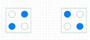
Fig.1. P = 1 and P = -1
Fig.1. explains the electron position in case of P = 1 and P = -1 polarization. Fig.2. enlightens the basic majority gate used for design F (A, B, C) = AB+BC+CA as well as AND gate (set C=0), OR gate (set C=1) using it.
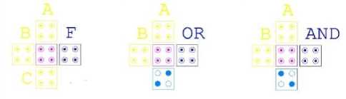
Fig.2. Majority Gate, OR, AND on QCA
QCA requires clocking mechanism for both combinational as well as sequential circuits which completely differ from traditional VLSI technology as prior one require clocking for only sequential circuits. Fig.3. illustrates four states of operation termed as switch, hold, release and relax lagging by π/2 in phase.
Clock zone 0
Clock zone 1
Clock zone 2
Clock zone 3
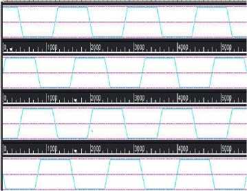
Fig.3. Clock zones in QCA
It’s being treated as the most efficient way to design reversible logic gates on ground of area and power efficiency.
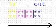
QCA wire can be said to be a clump of arranged cells holding same polarization and information flow between input and output due to the coulomb force of attraction acting in between them. Basically two QCA wire configuration exist in QCA [8] such that one is 90° and another is constructed by 45° cells.
Signal propagation
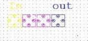
Fig.4. Normal Array or 90° QCA Wire and inverter Chain or 45° Wire
-
III. Key Terms
Constant inputs/Ancilla inputs: Specific set of input vectors set to binary 0 or 1 for circuit implementation is called constant inputs.
Garbage output: Additional output added in such a way that number of elements in input and output vectors become equal is called garbage output.
Quantum Cost: Quantum cost is the number of primitive gates (NOT, CNOT, V and V + ) used in the design. Where, V is the square root of NOT and V + is the hermitian of V following these axioms:
V * V = NOT(2)
V + *V + = NOT(3)
V * V + = V + *V = 1
Alternatively, area * latency 2 in quantum dot cellular automata also calculate quantum cost [9].
Flexibility: Flexibility can be termed as the how efficient a reversible logic is for performing several logical functions.
Delay: Delay is the maximum number of gate between input and output (on assumption of unit time taken by each gate for computing).
-
IV. Proposed Circuit
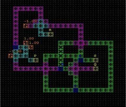
As per the requirement of lower garbage output, reduced area as well as complexity, a new reversible logic as per my survey named SA has been proposed here. It is basically a 4*4 Reversible Logic consisting of input vector(A,B,C,D) and output vector(P,Q,R,S) shown in fig. 5.
A
B
C
D
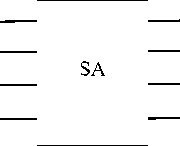
P= (A ⊕ B) C ⊕ AB ⊕ D
Q= A ⊕ B ⊕ C
R=(A ⊕ B)’C ⊕ A’B ⊕ D
S=B
Fig.5. SA Logic Block Diagram
The Truth Table of the proposed logic is expressed in Table 3.
Table 3. Truth Table of SA Logic
|
A |
B |
C |
D |
P=(A ⊕ B) C ⊕ AB ⊕ D |
Q=A ⊕ B ⊕ C |
R=(A ⊕ B)’ C ⊕ A’B ⊕ D |
S= B |
|
0 |
0 |
0 |
0 |
0 |
0 |
0 |
0 |
|
0 |
0 |
0 |
1 |
1 |
0 |
1 |
0 |
|
0 |
0 |
1 |
0 |
0 |
1 |
1 |
0 |
|
0 |
0 |
1 |
1 |
1 |
1 |
0 |
0 |
|
0 |
1 |
0 |
0 |
0 |
1 |
1 |
1 |
|
0 |
1 |
0 |
1 |
1 |
1 |
0 |
1 |
|
0 |
1 |
1 |
0 |
1 |
0 |
1 |
1 |
|
0 |
1 |
1 |
1 |
0 |
0 |
0 |
1 |
|
1 |
0 |
0 |
0 |
0 |
1 |
0 |
0 |
|
1 |
0 |
0 |
1 |
1 |
1 |
1 |
0 |
|
1 |
0 |
1 |
0 |
1 |
0 |
0 |
0 |
|
1 |
0 |
1 |
1 |
0 |
0 |
1 |
0 |
|
1 |
1 |
0 |
0 |
1 |
0 |
0 |
1 |
|
1 |
1 |
0 |
1 |
0 |
0 |
1 |
1 |
|
1 |
1 |
1 |
0 |
1 |
1 |
1 |
1 |
|
1 |
1 |
1 |
1 |
0 |
1 |
0 |
1 |
On considering the input vector as first set and output vector as another set as well as taking the decimal equivalent of the truth table we will obtain the fig.6, depicting the bijective nature of the logic.
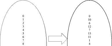
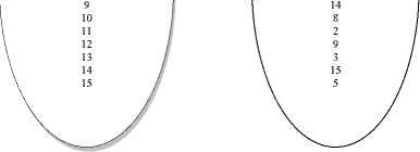
Input vector
Output vector
Fig.6. Bijective nature of proposed logic
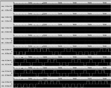
For the verification of the truth table QCADesigner 2.0.3 is taken in consideration and schematic as well as waveform is shown in fig.7.
(a)
(b)
Fig.7. SA Logic (a) schematic (b) waveform on QCA
Using this logic various combinational circuits like adder and subtractor can be designed. On treating D as constant input of 0 we can obtain full adder/subtractor circuit while on setting both C and D to a constant input of 0 we can obtain Half Adder /Subtractor circuit.
-
A. SA Logic as Full adder/Subtractor:
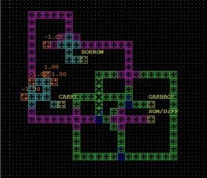
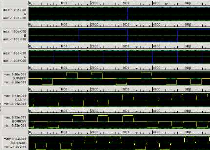
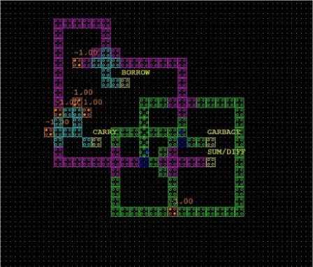
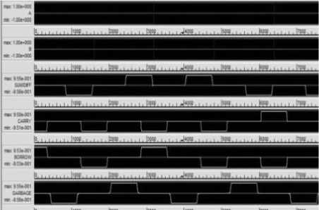
Full adder/ Subtractor are a combinational circuit performing addition/ subtraction for 3 inputs (A, B, C) and generating output as Sum/Diff, Carry and borrow; Table 4 shows its truth table. The full adder/subtractor can be implemented using the proposed SA logic if the fourth input bit i.e. D is set to 0 resulting in 3 inputs(A, B, C) , 3 outputs( sum/diff, carry, borrow) and 1 garbage bit. The QCA layout and waveform is shown in fig.8.
Table 4. Truth Table of FA/FS
|
A |
B |
C |
Sum/ Diff |
Carry |
Borrow |
|
0 |
0 |
0 |
0 |
0 |
0 |
|
0 |
0 |
1 |
1 |
0 |
1 |
|
0 |
1 |
0 |
1 |
0 |
1 |
|
0 |
1 |
1 |
0 |
1 |
1 |
|
1 |
0 |
0 |
1 |
0 |
0 |
|
1 |
0 |
1 |
0 |
1 |
0 |
|
1 |
1 |
0 |
0 |
1 |
0 |
|
1 |
1 |
1 |
1 |
1 |
1 |
(a)
(b)
Fig.8. SA logic as Full adder/ subtractor (a)schematic (b) waveform on QCA
-
B. SA Logic as Half adder/Subtractor:
Half adder/ Subtractor is a combinational circuit performing addition/ subtraction for 2 inputs (A, B) and generating output as Sum/Diff, Carry and borrow shown in table 5. In the proposed logic if third and fourth bit are set to zero value then it will act as a half adder/subtractor circuit consisting of 2 inputs(A, B), 3 outputs(sum/diff, carry, borrow) and 1 garbage outputs depicted in fig.9
Table 5. Truth Table of HA/HS
|
A |
B |
Sum/ Diff |
Carry |
Borrow |
|
0 |
0 |
0 |
0 |
0 |
|
0 |
1 |
1 |
0 |
1 |
|
1 |
0 |
1 |
0 |
0 |
|
1 |
1 |
0 |
1 |
0 |
(a)
(b)
Fig.9. SA logic as Half Adder/Subtractor (a)schematic (b) waveform on QCA
-
V. Results and Discussion
For the sake of verifying the proposed circuits some of the parameters have been taken in consideration shown in fig.10. These are by-default criterion in QCADesigner [10]. The proposed circuit has been designed in single layer and consists of coplanar wire crossing. Its effective area is 0.17µm2 consisting of 137 cells.
Table 6. Comparative Analysis of Reversible Full Adder/ Subtractor Circuit
|
No. of Gates Used |
No. of garbage Output |
No. of Constant Input |
Circuits Formed |
Tool Used |
|
|
Design 1 [13] |
8 |
5 |
3 |
1(Full Adder) |
Xilinx |
|
Design 2 [13] |
4 |
3 |
1 |
1(Full Adder) |
Xilinx |
|
Design 3 [13] |
4 |
3 |
1 |
1(Full Adder) |
Xilinx |
|
Fredkin Gate [14] |
6 |
5 |
4 |
1(Full Adder) |
- |
|
DKG Gate [15] |
1 |
2 |
1 |
2(Full Adder, Full Subtractor) |
Xilinx |
|
TSG Gate [16] |
1 |
2 |
1 |
1(Full Adder) |
Tanner |
|
OTG Gate [17] |
1 |
2 |
1 |
1(Full Adder) |
- |
|
Inventive0 Gate [18] |
1 |
2 |
1 |
2(Full Adder, Full subtractor) |
Microwind DSH-2.7 |
|
DG[19] |
2 |
2 |
1 |
1(Full Aubtractor) |
QCA |
|
TG[20] |
2 |
2 |
1 |
1(Full Subtractor) |
- |
|
Feynman and Peres gate[21] |
4 |
3 |
1 |
2(Full Adder, Full Subtractor) |
- |
|
Peres Gate[22] |
2 |
2 |
1 |
1(Full Adder) |
Tanner EDA with TSMC018 Technology |
|
Peres Gate[23] |
2 |
2 |
1 |
1(Full Adder) |
Xilinx ISE |
|
IG Gate[24] |
2 |
2 |
2 |
1(Full Adder) |
- |
|
New , toffoli, Feynman gate[25] |
3 |
3 |
1 |
1(Full Adder) |
- |
|
Fredkin gate[26] |
4 |
3 |
2 |
1(Full Adder) |
- |
|
Proposed Design |
1 |
2 |
1 |
2(Full Adder, Full Subtractor) |
QCA |
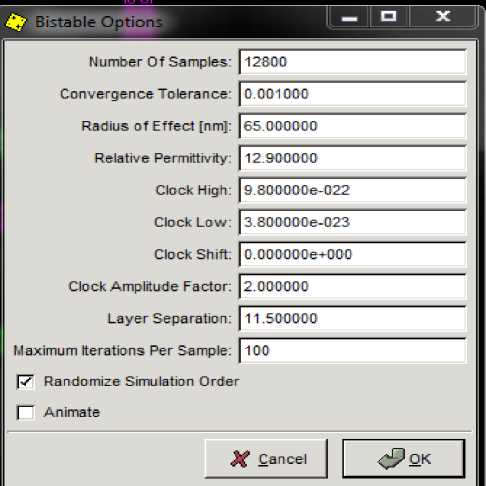
Fig.10. QCADesigner Parameters
Energy dissipation can be calculated using QCA Designer–E [11] on considering parameters shown in fig.11.
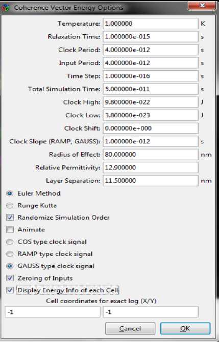
Fig.11. QCADesigner-E coherence vector energy option
QCADesigner-E is actually simulation module of QCA Designer, the parameter description can be seen from data sheet [12]. The simulation result display on enabling the option of display energy info of each cell in the coherence vector simulation as shown below:
Sum_bath: S 7.98e-002
S -7.72e-003
bE
Avg_bath: A 7.25e-003
A -7.02e-004
bE
Sum_clk: S -1.29e-002,
Avg_clk: A -1.18e-003
Comparative Analysis:
After a rigorous review of various papers comparative analysis of the proposed Full Adder/Subtractor design with some of the existing ones is enlisted in Table 6. This table demonstrates that the proposed design is capable of implementing reversible full adder/subtractor circuit on QCA using single gate, minimal garbage output as well as constant input.
-
VI. Conclusion
This paper presents a QCA layout of SA logic, applicable in designing of various combinational circuits like half adder, full adder, half subtractor and full subtractor with minimal garbage output. The simulation result confirms the operation of the design using the ideal bi-stable options. This, design can be a good move in the combinational circuits design. The proposed SA logic can be used in application of ALU designing for arithmetic operations as well as it can be used in bus interface unit i.e. for physical address generation etc.
References An optimized approach towards reversible adder/subtractor design on QCA
- Snigdha Singh, Abhinay Choudhary, Manoj Kumar Jain, "A Brief Overview of Reversible Logic gate and Reversible Circuits," International journal of Electronics Engineering, volume 11,Issue 2 June - Dec 2019 pp.. 86-104.
- Gordon E. Moore," Cramming more components onto integrated circuits,"Electronics, volume 38, number8, April 19, 1965.
- R. Landauer, "Irreversibility and Heat Generation in the Computing Process," in IBM Journal of Research and Development, vol. 5, no. 3, pp. 183-191, July 1961.
- W. Keyes & R. Landauer,“Minimum Energy Dissipation in Logic,” IBM Journal of Research and Development. 14. 152-157. 1970.
- C. H. Bennett," Logical Reversibility of Computation," IBM Journal of Research and Development, vol. 17, no. 6, pp. 525-532, Nov. 1973.
- Robert Wille, Rolf Drechsler, "Towards a Design Flow for Reversible Logic," Springer book.
- Massimo Macucci,"Quantum Cellular Automata (QCA) Theory, Experimentation and Prospects,"Copyright © 2006 by Imperial College Press ISBN 1-86094-632-1Printed in Singapore by World Scientific Printers (S) Pie Ltd.
- V. Vedral, A. Bareno and A. Ekert, “Quantum networks for elementary arithmetic operations”, Physical Review A, vol. 54, no. 1, (1996), p. 147
- Md. Abdullah-Al-Shafi, Riasaad Haque Aneek , Ali Newaz Bahar," Universal Reversible Gate in Quantum-Dot Cellular Automata (QCA): A Multilayer Design Paradigm," International Journal of Grid and Distributed
- K. Walus, T. J. Dysart, G. A. Jullien and R. A. Budiman, “QCADesigner: A rapid design and simulation tool for quantum-dot cellular automata”, IEEE transactions on Nanotechnology, vol. 3, no. 1, (2004), pp. 26-31.
- F. Sill Torres, R. Wille, P. Niemann and R. Drechsler, "An Energy-Aware Model for the Logic Synthesis of Quantum-Dot Cellular Automata," in IEEE Transactions on Computer-Aided Design of Integrated Circuits and Systems, vol. 37, no. 12, pp. 3031-3041, Dec. 2018.
- Manual for QCADesigner-Energy (QD-E) Manual version: 1.0(https://github.com/FSillT/QCADesigner-E)
- Rangaraju H G , Venugopal U , Muralidhara K N , Raja K B ," Low Power Reversible Parallel Binary Adder/Subtractor," International Journal of VLSI Design & Communication Systems, 1.3(2010),pp-23-34.
- W. D. Pan and M. Nalasani, "Reversible logic," IEEE Potentials, vol. 24, no. 1, pp. 38-41, Feb.-March 2005.
- B.Raghukanth, B.Murali Krishna , M. Sridhar and V.G. SanthiSwaroop"a distinguish between reversible and conventional logic gates,"Journal of Engineering Research and Applications (IJERA) Vol. 2, Issue 2,Mar-Apr 2012, pp.148-151.
- S. S. Chiwande and P. K. Dakhole, "VLSI design of power efficient Carry Skip Adder using TSG & Fredkin reversible gate," 2012 International Conference on Devices, Circuits and Systems (ICDCS), Coimbatore, 2012, pp. 370-373.
- M. Surekha," Efficient Approaches for Designing Quantum Costs of Various Reversible Gates," International Journal of Engineering Studies. ISSN 0975-6469 Volume 9, Number 1 (2017), pp. 57-78.
- Neeraj KumarMisra, Mukesh Kumar Kushwaha, SubodhWairya&Amit Kumar (2015), "Cost Efficient Design of Reversible Adder Circuits for Low Power Applications,” International Journal of Computer Applications. 117. 37-45. 10.5120/20665-3408.
- Jadav Chandra DAS and Debashis DE," Reversible binary subtractor design using quantum dot-cellular automata” Frontiers of Information Technology & Electronic Engineering www.jzus.zju.edu.cn; engineering.cae.cn; www.springerlink.com ISSN 2095-9184 (print); ISSN 2095-9230 (online). 2017 18(9):1416-1429
- Himanshu Thapliyal and Nagarajan Ranganathan," Design of Efficient Reversible Binary SubtractorsBased on A New Reversible Gate,” 978-0-7695-3684-2/09 $25.00 © 2009 IEEEDOI 10.1109/ISVLSI.2009.49.
- Anamika and R. Bhardwaj,"Reversible logic gates and its performances,"2018 2nd International Conference on Inventive Systems and Control (ICISC),Coimbatore, 2018,pp. 226-231.
- P.Vanusha , k.AmurthaVally," Low Power Computing Logic Gates design using Reversible logic," International Journal of Application or Innovation in Engineering & Management (IJAIEM) Volume 3, Issue 10, October 2014..
- S. R. S. Kalavakolanu," Implementation of Reversible Logic at Gate Level," 2018 2nd International Conference on Inventive Systems and Control (ICISC), Coimbatore, 2018pp.959-963.
- M. S. Islam, M. M. Rahman, Z. Begum and M. Z. Hafiz, "Fault tolerant reversible logic synthesis: Carry look-ahead and carry-skip adders," 2009 International Conference on Advances in Computational Tools for Engineering Applications, ZoukMosbeh, 2009, pp. 396-401.
- H. M. H. Babu, M. R. Islam, S. M. A. Chowdhury and A. R. Chowdhury, "Synthesis of full-adder circuit using reversible logic," 17th International Conference on VLSI Design. Proceedings., Mumbai, India, 2004, pp. 757-760.
- J. W. Bruce, M. A. Thornton, L. Shivakumaraiah, P. S. Kokate and X. Li, "Efficient adder circuits based on a conservative reversible logic gate," Proceedings IEEE Computer Society Annual Symposium on VLSI. New.
