Area & power optimization of asynchronous processor using Xilinx ISE & Vivado

Author: Archana rani, Naresh Grover
Journal: International Journal of Information Engineering and Electronic Business @ijieeb
Article in issue: 4 vol.10, 2018.
Free access
As the technology era has been changing, the designing pattern of an IC is also changing. An IC de-signing is now divided into two definite fields i.e. Front-End design and Back-End design. The Front-End design is using HDLs (Hardware Description Languages i.e. VHDL or Verilog) and the verification of those ICs, whereas the Back-End Design is related to the Physical Design techniques. But both of the IC design techniques required some extra efforts in terms of their Speed, Shape, and Size, which needs the Optimization efforts. This pa-per deals with the area and power optimization efforts in terms of the logic utilization by using XST & Vivado Tools. After applying area optimization techniques i.e. Logic Optimization, LUT mapping and Resource Sharing etc. on already designed asynchronous microprocessor to be used as model for proposed optimization, reasonable results in terms of power and area utilization have been achieved.
FPGA, Microprocessor design, Optimiza-tion, Xilinx Synthesis Tool (XST) and Vivado
Short address: https://sciup.org/15016138
IDR: 15016138 | DOI: 10.5815/ijieeb.2018.04.02
Text of the scientific article Area & power optimization of asynchronous processor using Xilinx ISE & Vivado
Published Online July 2018 in MECS
An IC design engineer has to always go through the beneath of the design logic to the commercialized view of the Fabricated IC. Though, this process requires lots of creativity, enthusiasm and efforts and all of that in a specified time of the frame. The Time-of-Frame is the keynote for any kind of the new IC design approach. Thanks to VLSI technology advancement that we are in an era where we can choose either the early phase of the design or the last phase of the design. Every design phase has their limitations and challenges. This work is much focused on the front-end part of the IC design technology by using FPGAs. Now a day’s FPGA is the need for the digital systems design. The main reasons for using FPGAs in modern digital system designs are:
-
• Design Test & Check: The reconfigurability of FPGAs provides a working chip immediately, once programmed and configured.
-
• Prototyping: The FPGAs can be used as a final design prototyping. It can be used as the final design from prototype to product, which is much easier and always reduces the budgeting.
-
• Reprogrammable: The single FPGA device can be utilized in various designs and reduces the NRE costs.
This paper shows the features of FPGA based digital system design, their primary goals and techniques, the major challenges while designing with the FPGAs. The optimization techniques and design tools for that purpose. The complete work has been carried out on the 32-bit Asynchronous Processor which previously designed by us.
-
II. FPGA - Based Digital System Design
The uses of FPGAs are increasing exponentially for Digital System design because of their reprogrammable and reconfigurable feature while on the field. Also, there are various fields of the FPGA family’s availability in the present scenario. However, now-a-days FPGAs have various features that make them adaptable to all types of available technologies. But also it is bitter truths that while choosing the FPGAs, the designer always has to set their primary objectives (specifications). Some of the objectives are discussed below:
-
A. Goals and Techniques
The foremost objective that should be achieved by an FPGA based digital system design is the Logical function that is going to be implemented. For this, the designer may opt various digital design technologies in order to achieve the desired operation.
-
i. Performance: The performance is another objective that should be achieved either in terms of the throughput and latency. However, most of the time it is measured by the Clock rate of the design .
-
ii. Power/Energy: Most of the digital based system designs are Battery Powered. Thus, the chip should have some energy or power budget. The system always
dissipates some Energy even if the system is not on the direct power rails. Thus the heat dissipation increases money and must be controlled.
-
iii. Design Time & Cost: The design time always plays a critical role while writing the logic designs. The design time must be control by FPGAs because they are standard parts. The FPGAs have numerous advantages in design time. They can be used as a separate component in the final design, they can also be used as a prototype and they can be programmed quickly. The design time is one important component of the design.
-
B. Design Challenges
-
i. Multiple levels of abstraction: The digital system design always requires the refining of its working through many levels of details. The design always starts from the specification of the system must do; the designer then creates an architecture which performs the required functions and then breaks the architecture into a logic design.
-
ii. System Design Costs: The design costs also matters with the use of software needed to design and may also be in performance or power consumption of the final FPGA based system.
-
iii. Design time: As the competitive electronics market is growing, the design time for the chip must be faster in order to reduce NRE costs and to increase the revenue.
-
C. Requirements and specifications:
The term requirement means a written description of what the system is to do - for example “Asynchronous Processor design”, in this paper. Also, the term specification is the more formal description of the function, such as simulation results of the functionality. Attributes, like Device Utilization, power consumption. Processor specification: 32-bit data, 32-32-bit temporary registers, RAM or ROM blocks.
-
III. Design Example of Processor Architecture
The asynchronous processor internal operation is segmented into five pipeline stages and in each of them the operations of the tasks will be performed in the normal (identified with the ID block), execution of the operation (identified with the EX block), memory access (identified
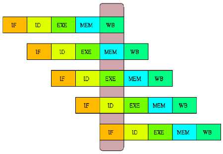
Fig.1. Processing Stages cycle of an instruction, i.e. search of the instruction (identified with the IF block), decoding of The instruction with the MEM block) and storage of the operation result (identified with the WB block).
-
A. Feature of Naval Processor Architecture
The 32-bit asynchronous processor has the capability of handling all types of instructions i.e. I-Type, R-Type, Jump Instructions and also multiply instructions packet. The multiplied result is stored until is needed irrespective of other instructions follows. The proposed processor is using separate memory for instructions and Data. The capacity of instruction memory i.e. ROM is of 8192*32 in which 8192 are representing the locations where instructions are to be stored with 32-bit data. The structures of instructions are as per ISA (instruction set Architecture). For all stages, there is only one clock cycle needed, while the data memory has the capacity of 64K. Both memories are functioning in falling pulse. The other pulses are used for developing the necessary functions just like pipelining in order to make our processor core faster and much flexible. All I-type instructions are part decoded in the first stage and all R-type instructions are part decoded in ALU control unit. This reduces the complexity of main control unit. The complete processor core is designed in Xilinx ISE 14.x tool. The so far studied processor architectures do not contain all instruction in a single architecture especially (Jump & Multiply instructions). Also while designing the whole processor core much more attention is given to design the proposed processor in such a way to optimize the core for much better results in terms of Area, Power or Delay.
Figure 2 shows the internal architecture of Asynchronous processor, In this processor, fetching the instruction pointed by the Program counter goes to the next unit called decoder which generates the different values of the memory location, as per the instruction fetched from the previous unit. During this control unit has been designed in order to synchronize the various other units such as ALU, data memory or general purpose registers to properly execute the desired instruction. There are other units named as ALU, data memory, and some multiplexers to complete the execution cycle.
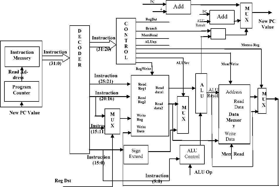
Fig.2. Internal Architecture of Asynchronous Processor
Each FPGA device contains the LUTs as their basic logic implementation unit. Now a day there are various FPGA families available in the market. Each FPGA device has different internal orientation some are also embedded with some hardcore or soft-core processor architecture, Clock management tiles, large DSPs Slices for high-speed multiplication, RAM or ROM blocks etc. Every time the designer has to well equip with the internal organization of the selected FPGA device(s). In order to create or design their logic in such a way that the digital system must be adaptable to any selected FPGA device, the design must fully utilize the internal resources of the FPGA Fabrics, the Placement and Routing of the entire internal cells must be cleared by the DRC etc. Thus the optimization of any logic is still a very wide area of interest for many FPGA designer and researchers. Although the optimization algorithm always upgraded or enhanced by the researchers the basic classification is the same.
In order to write complex circuit description, the designer must ensure that the logic meets all the nonfunctional requirements while maintaining its logical correctness. The designer does this today by using the tools, which help them to optimize a logic description. Initially, the designer has to describe the logical function as simple as possible. The designer then relies on optimization tools to transform that logical description to meet their other goals without breaking the original functions. It is important to have a basic understanding of how these tools work in order to make the best use of them. To obtain the desired results doesn’t mean that the designer simply clicks the Synthesis option in available EDA Tool. For the desired results the designer must have the knowledge of how the tools work. There are some techniques discussed below:
-
A. Mapping to an FPGA
This is the foremost thing a designer must use to do. They clearly have to choose an FPGA to map their design into it. The knowledge of the FPGA brand & family of FPGA is not enough to transform the logic into a configuration. As there are various FPGA families available with different numbers of logic elements (which also changes the amount of interconnect on the chip); different numbers of I/O pins. The FPGA size is generally described by the number of Logical Elements (LEs) or LUTs and the number of pins on the device. Most of the time, the LEs on the chip relative to the number of pins. Also, it may possible, that the same number of pins may be provided in more than one type of package. The chip may have several LEs in terms of Primitive blocks i.e. Accumulator, RAM or ROM blocks, DSP blocks, and Multipliers etc. It is the responsibility of the designer to use or choose them properly when the optimization is the primary concern. This type of optimization is also known as LUT or Technology mapping.
-
B. Logic Optimization
Writing the logical function to build in hardware is the first step in digital design. It is also known as logic synthesis. It is basically a rewriting process to improve the nonfunctional characteristics of logic size performance and/or power while maintaining its primary function. The logic optimization can be used either in the combinational circuits or sequential circuits. The combinational circuit can be optimized by using the laws of Boolean algebra to simplify the logic or may use don't cares to improve the logic or may also add common factors to reduce the size or eliminate levels of logic to increase performance without disturbing their primary functionality. While, the sequential circuit can be optimized by using the safe implementation of FSM, by providing the synchronous reset for the proper functioning of the states.
-
C. Physical Optimization
The physical optimization always comes into action after the designer has rewritten the logical functions for the selected device. Most of the time, it is Technology specific i.e. as per the Target Device. Basically, this optimization is divided into placement and routing of the design on the chip. This optimization mostly used to be done by the synthesis tool only. During the Placement phase, the available gates are selected to implement each piece of the logic. Also in this, the designer can use the LUT combining for merging the LUT pairs with same inputs into single dual- multiple output LUTs in order to improve design area. However, it may reduce the design speed. During the Routing, it binds the various logical gates in order to achieve the proper performance. It is basically used when the timing requirement is much necessary.
-
V. Optimization Using XST
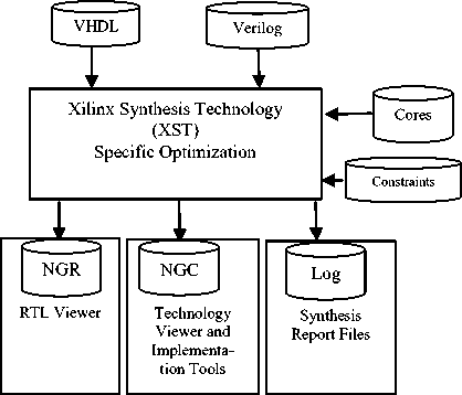
Fig.4. The Flow of Files through the XST software
XST is using in Xilinx ISE tool where a designer uses to enter their logic in textual format with the help of HDLs i.e. VHDL or Verilog. As for any type of optimization such as a Sequential circuit or combinational circuit optimization designer have to provide some constraints e.g. don’t care conditions, FSM extraction etc. Sometimes they also use the block primitives which are named as IP core for any specific FPGA device. After providing all these details we get two graphical output i.e. RTL viewer and Technology-specific viewer and one text log files.
-
A. XST Detailed Design Flow
The following figure 5 shows each of the steps that take place during XST synthesis. The following sections describe each step in detail.
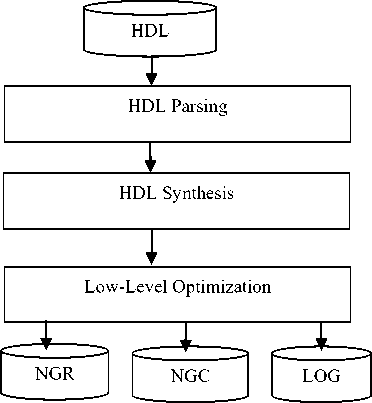
Fig.5. XST Detailed Design Flow
In the first stage, XST checks the correctness for in the VHDL/Verilog code and then generates the report which may contain the Syntax errors. This is known as HDL Parsing. Next XST analyzes the HDL codes in order to generate specific building blocks e.g. MUXs, RAMs, Adders etc. So in this way, it creates an efficient technology implementations environment. Sometimes XST also conducts a resource sharing check in order to reduce the amount of inferred building blocks or macros this may reduce the area and increases the clock frequency. The XST also performs the Finite State Machine (FSM) recognition during HDL synthesis. In order to generate the most efficient implementation, there should be target optimization goals in terms of Area or Speed. For generating the efficient optimization we have to set the global parameters, such as the optimization goal or effort level. We modify the synthesis properties in the Synthesize Process Properties dialog box.
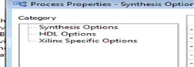
Fig.6. Synthesis Option Properties
The use of technology-specific features may come from a macro implementation mechanism or from general logic mapping. Due to mapping complexity issues, not all available FPGA features may be used. The FPGA synthesis flow supports advanced design and optimization techniques, such as Register Balancing.
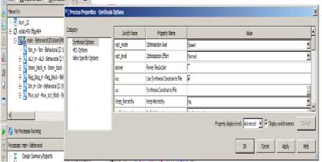
Fig.7. Global Parameters Settings in XST
-
VI. Results Analysis
In This paper, work is based on same optimization rules as discussed in previous sections. All rules are applied on 32-Bit Asynchronous Processor with Xilinx XST. This section shows enhancement of design in terms of area and power. This work has been carried out on SP605 Evolution Board for design implementation. However, this design and its optimization are so generalized that it can adhere to any FPGA family. The design also implemented and optimized using Vivado for Virtex-7 FPGA device.
At the Low-Level Optimization step, XST performs the technology-specific implementation by transforming the generated building blocks or macros and general glue logic. The glue logic is different for the FPGAs and CPLDs. During low-level optimization for FPGAs, XST infers specific components, such as the following:
-
• Carry logic (MUXCY, XORCY, MULT_AND)
-
• RAM (block or distributed)
-
• Shift Register LUTs (SRL16, SRL32)
-
• Clock Buffers (IBUFG, BUFG, BUFGP, BUFR)
-
• Multiplexers (MUXF5, MUXF6, MUXF7,
MUXF8)
-
• Arithmetic Functions (DSP48, MULT18x18)
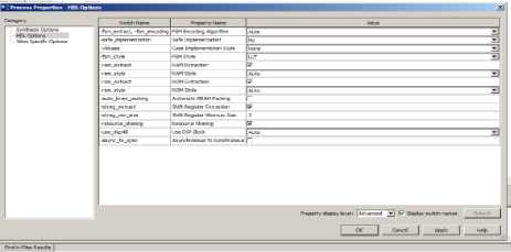
Fig.8. Logic Optimization using XST
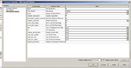
Fig.9. Advanced Optimization Technique using XST
Table 1. Post Synthesis Device Utilization using XST -Before Optimization
|
Logic Utilization |
Used |
Available |
|
Number of Slice Register |
1991 |
54576 |
|
Number of Slice LUTs |
2165 |
27288 |
|
Number of Fully used LUT-FFs- Pairs |
833 |
3226 |
|
Number of Block RAM/FIFOs |
5 |
116 |
|
Number of DSP48A |
4 |
58 |
Table 2. Post Synthesis Device Utilization using XST- After Optimization
|
Logic Utilization |
Used |
Available |
|
Number of Slice Register |
1652 |
54576 |
|
Number of Slice LUTs |
1921 |
27288 |
|
Number of Fully used LUT-FFs- Pairs |
739 |
3226 |
|
Number of Block RAM/FIFOs |
38 |
116 |
|
Number of DSP48A |
4 |
58 |
Figure 10 shows that before applying the optimization the resources are used but due to not proper LUT mapping, it shows the less condensed utilization. And it also may be due to the improper code or logic mapping as per the target FPGA device i.e. SP-605.
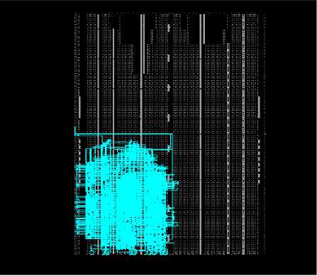
Fig.10. Post Implementation view using FPGA editor - Before Optimization
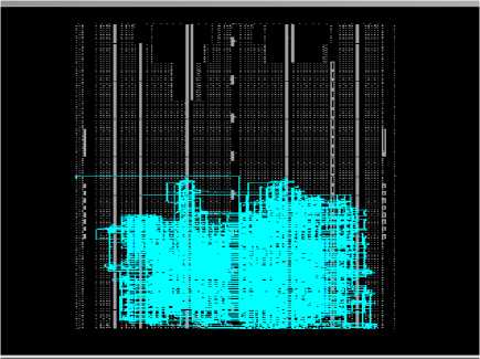
Fig.11. Post Implementation view using FPGA Editor- After Optimization
The figure 11 shows that after applying the optimization rules the design is more condensed and fully placed and routed.
Utilization - Post-Synthesis
|
Resource |
Estimation |
Available |
Utilization % |
|
|
LLFT |
1720 |
303600 |
0.57 |
|
|
FF |
1618 |
607200 |
0.27 |
|
|
ERAM |
6 |
1030 |
0.58 |
|
|
DSP |
4 |
2800 |
0.14 |
|
|
IO |
40 |
600 |
6.67 |
|
|
EUFG |
5 |
32 |
15.62 |
|
Fig.12. Post Synthesis Device Utilization by Vivado before Optimization.
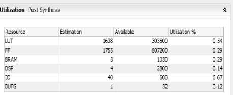
Fig.13. Post Synthesis Device Utilization by Vivado- After Optimization.
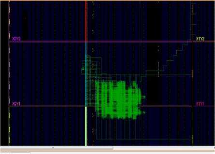
Fig.14. Post Implementation – Before Optimization
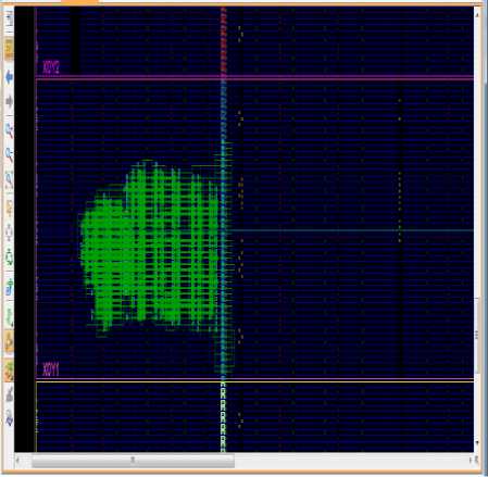
Fig.15. Post Implement Design – After Optimization.
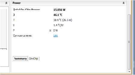
Fig.16. Power Summary- Before Optimization
Total On-Chip Power:
Junction Temperature:
Thermal Margin:
Effective itiA:
3ower supplied to off-chip devices
Confidence level:
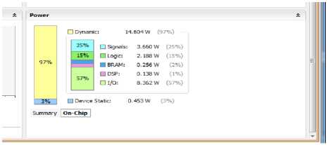
Fig.17. On-chip Power Summary- Before Optimization
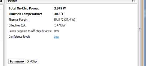
Fig.18. Power Summary – After Optimization
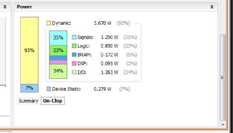
Fig.19. On-chip Power summary- After Optimization
-
VII. Conclusion
FPGAs are the most advent devices for digital system design consideration because of its cost and reprogram ability. By taking these things into consideration this work is designed for 32-bit asynchronous processor system. After complete synthesization and simulation using Xilinx ISE and Vivado, work have been started for Area Optimization for the previous design. After researching various papers, Logic Optimization, LUT mapping, Resource Sharing, Register Balancing has been applied.With the use of these optimization techniques the logic has been optimized considerably 7-12% and also improved power response. However, In future, this can be further optimized by using recent or upcoming techniques. Also, this work can be further expanded by using the fault tolerant scheme such as TMR(Triple mode redundancy), BCH codes.
References Area & power optimization of asynchronous processor using Xilinx ISE & Vivado
- Matthew French, Li Wang, Tyler Anderson, Michael Wirthlin “Post Synthesis Level Power Modeling of FPGAs” Proceedings of the 13th Annual IEEE Symposium on Field-Programmable Custom Computing Machines (FCCM’05) 2005 IEEE.
- Maico Cassel, Fernanda Lima Kastensmidt “Evaluating One-Hot Encoding Finite State Machines for SEU Reliability in SRAM-based FPGAs” Proceedings of the 12th IEEE International On-Line Testing Symposium (IOLTS'06)
- Jason Cong Bin Liu, Stephen Neuendorffer, Juanjo Noguera, Kees Vissers, and Zhiru Zhang “IEEE Transactions On Computer-Aided Design Of Integrated Circuits And Systems, VOL. 30, NO. 4, April 2011.
- B.G. Kim, and D.L. Dietmeyer, "Multilevel logic synthesis of symmetric switching functions," IEEE Trans. on CAD, Vol. 10, No. 4, pp. 436-446, April 1991.
- L. Yan, T. Srikanthan, and N. Gang, “Area and Delay Estimation for FPGA Implementation of Coarse-Grained Reconfigurable Architectures,” LCTES, Ottawa, Ontario, Canada,pp.182–188, 2006.
- D. Kulkarni, Walid A. Najjar, R. Rinker and F. J. Kurdahi,“Compile-Time Area Estimation for LUT-Based FPGAs,” ACMTODAES, Vol. 11, No. 1, pp. 104–122, 2006.
- A. Mishchenko, S. Chatterjee, R. K. Brayton, “Improvements to Technology Mapping for LUT–Based FPGAs,” IEEE Trans. on Computer-Aided Design of Integrated Circuits and Systems, Vol. 26, No. 2, pp. 240–253, Feb. 2007.
- D. Chen, J. Cong, Y. Fan, and Z. Zhang, “High-Level Power Estimation and Low-Power Design Space Exploration for FPGAs,”ASPDAC’0, Yokohama, Japan, pp. 529-534, 2007.
- Pablo González de Aledo Marugán, Javier González-Bayón and Pablo Sánchez Espeso, “Hardware performance estimation by Dynamic Scheduling” ;in Proc. FDL, 2011, pp.1-6.
- Michael Kunz, Martin Kumm, Martin Heide, Peter Zipf, “Area Estimation of Look-Up Table Based Fixed-Point Computations on the example of a Real-Time High Dynamic Range Imaging System" In 22nd International conference on Field Programmable Logic and Applications(FPL), pages 591-594, Aug 29-31 2012.
- A. M. Smith, G. A. Constantinides, and P. Y. K. Cheung, “Integrated floorplanning, module-selection, and architecture generation for reconfigurable devices,” IEEE Trans. on Very Large Scale Integration (VLSI) Systems, vol. 16, no. 6, pp. 733–744, Jun 2008.
- J. Luu, I. Kuon, P. Jamieson, T. Campbell, A. Ye, M. Fang, and J. Rose, “Vpr 5.0: FPGA CAD and architecture exploration tools with single-driver routing, heterogeneity and process scaling,” in Int’l Symp. on Field-Programmable Gate Arrays, Feb. 2009, pp. 133–142.
- E. Ahmed and J. Rose, “The effect of LUT and cluster size on deep-submicron FPGA performance and density,” IEEE Trans. on Very Large Scale Integration (VLSI) Systems, vol. 12, no. 3, pp. 288–298, Mar. 2004.
- H. Q. Dao, B. R. Zeydel, V. G. Oklobdzija: "Energy minimization method for optimal energy-delay extraction" Proceedings of European Solid-State Circuits Conference, p. 177-180, 2003.
- Naresh Grover, M.K.Soni,” Simulation and Optimization of VHDL code for FPGA-Based Design using Simulink” I.J. Information Engineering and Electronic Business, 2014, 3, 22-27.
