Bio-chip design using multi-rate system for EEG signal on FPGA

Author: Nazifa Tabassum, Sheikh Md. Rabiul Islam, Xu Huang
Journal: International Journal of Image, Graphics and Signal Processing @ijigsp
Article in issue: 4 vol.10, 2018.
Free access
Digital Signal Processing (DSP) is one of the fastest growing techniques in the electronics industry. The signal-rate system in digital signal processing has evolved the key of fastest speed in digital signal processor. Field Programmable Gate Array (FPGA) offers good solution for addressing the needs of high performance DSP systems. The focus of this paper is on the basic DSP functions, namely filtering signals to remove unwanted frequency bands. Multi-rate Digital Filters (MDFs) are the main theme to build bio-chip design in this paper. For different purposes DSP systems need to change the sampling rate of the signal to achieve some applications. This can be done using multi-rate system where designers can increase or decrease the operating sampling rate. This bio-chip has attractive features like, low requirement of the coefficient word lengths, significant saving in computation time and storage which results in a reduction in its dynamic power consumption. This paper introduces an efficient FPGA realization of multi-rate digital filter with narrow pass-band and narrow transition band to reduce noises and changing the frequency sampling rate by factor which is required according to application. This bio-chip works on bio-signals like EEG signal.
Bio-chip, Multi-rate, Decimate, Interpolate, EEG
Short address: https://sciup.org/15015955
IDR: 15015955 | DOI: 10.5815/ijigsp.2018.04.05
Text of the scientific article Bio-chip design using multi-rate system for EEG signal on FPGA
Published Online April 2018 in MECS DOI: 10.5815/ijigsp.2018.04.05
Electroencephalogram (EEG) is signal with electrical activities of human cognition states [1]. The measurement of these electrical activities can be taken from different locations on the scalps [2] - [4]. The EEG signal involve noises and artifacts during the recording of EEG signal. The noise from the main source like electro-oculogram (EOG), electrocardiogram (ECG), electromyogram (EMG) and other sources should be eliminated to increase accuracy of bio-signal processing in bio-chip system. However, there is no need to consider high speed processing and has no effect on the analysis data with a minimum delay the data measurement procedure [10]. For real time EEG signal analysis, it is argued that software processing is not sufficient and hardware processing needs to be involve. Hardware processing is fast and can provide portability due its small size. However, it may produce less accurate results than the software processing because of the appearance of quantization errors. [16].
The most of bio-system has got physiological artifacts due to the variety of body activities such as body movements, skin resistance fluctuations or other bioelectrical potentials. From this aspect researcher raise the question how to develop digital filter chip to remove these artifacts. The FPGA is employed in the analysis of EEGs in this project to perform smooth EEG signal based on the proposed biochip on multi-rate system. The proposed biochip design on multi-rate system is worked with sampling rate conversion for high speed data and lower time resolution. The main concept of this biochip systems is used to change the sampling rate of a signal. The process of sampling rate decrease is called decimation, and the process of sampling rate increase is called interpolation [5], [6].
The main approach of this system is to change the sampling rate of the EEG signals and convert it back into analog and then to re-digitize it at a new rate. The quantization and aliasing errors inherent in digital-analogdigital conversion processes, would degrade the signal. This paper uses multi-rate processing for changing the sampling frequency rate of a signal digitally. Its main attraction is that it allows the strengths of a conventional DSP to be exploited. For example, much of the antialiasing and anti-imaging filtering in real time DSP systems can be performed in the digital domain, enabling both sharp magnitude frequency as well as linear phase responses to be achieved.
The system has a computer where the design can be programmed and simulated on Xilinx Integrated Software Environment (ISE) Suite 13.2 or Quartus II software with interface ALTRA Cyclone DE II board of FPGA device . From the implementation side, references [7], [8], [9], use Xilinx chips and Altera devices [10].
This paper is organized as follows. A brief description on materials and methods based on proposed biochip design on multi-rate system in section II. In section III, obtained experimental results are analyzed and consequent issues are discussed. Finally, conclusions are described in section IV.
-
II. Materials and Methods
-
A. Database
The data of signals are collected from BME signal processing lab from dept. of Biomedical Engineering of KUET. The data is taken on Electroencephalogram (EEG). The biopac system interface with human body and PC. The patient age was 22 and they are all students. The condition was solving puzzle for recording EEG signal.
-
B. Proposed Methodology of Multi-rate system
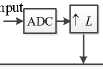
The proposed multi-rate system has considered sampling rate conversion (SRC) for biomedical medical signal processing applications. The way to SRC is to connect an ADC in series with a DAC to first convert the continuous signal x(t) to a discretesequence x[n] and then back into the analog domain at the new sampling rate f snew . Due to spectral distortion is induced by a ADC conversion followed by an DAC conversion, this method is typically avoided in practice. The better alternative are all digital solutions. There are three kinds of SRC: decreasing sampling rate (called Decimation f s,new < f s,oid ), increasing it (called
Interpolation, f s,new > f s,old ), synchronizing two signals with the same sampling frequency (f, , new = f s,old ). So, we have considered three different cases as shown in Fig. 1 where case(i) uses first increasing sampling rate by L of discrete signal x[n] and then uses digital filter and after that decreasing the sampling rate by M, where L=M; (ii) just opposite of case (i) i.e. decreasing the sampling rate of x[n] by M and filter of it and then increasing the sampling rate of filtered signal where M=L; and finally for case(iii) L ^ M.
-
Case I:
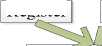
A simple block diagram representation of the proposed multi-rate system is given in Fig. 1. where h(k) is an antialiasing digital filter. This proposed system is considered direct from FIR filter implementation, the output of the filter, y(n) and the input x(n),
У(п) = Z^h^Mn - k) (1)
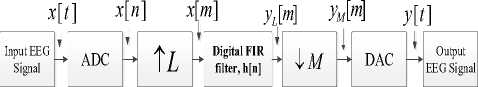
Fig.1. Block diagram of proposed biochip on multi-rate system for Case
I.
The proposed biochip on multi-rate system have assigned some paprameters on input-output relationship for each block as in Fig. 1 and its signal flow graph is shown in Fig. 2. For every input sample, x(n) fed into the interpolator, the rate expendure the box with an up arrow in search L-1 zero valued samples after the input samples.Thease are then filtered to yield y(m). Thus for each input samples for x(n), L samples of y(m). Effectively, the input sampling frequeny is increased from fs to Lfs by the interpolator. One implication of inserting
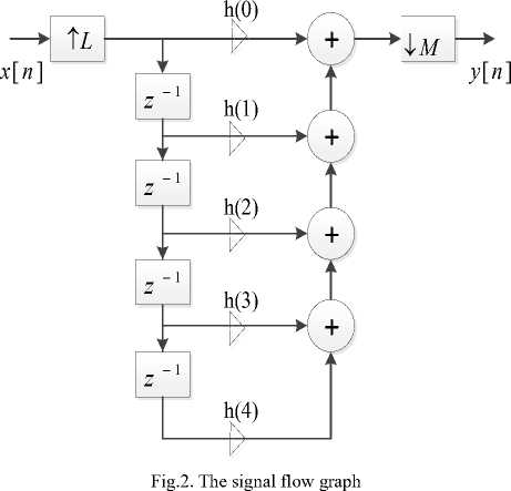
Each input sample fed in, three samples are computed. The non zero samples (that is the actual samples of x(n) in the delay line are seperated by L-1 zeroes). Clearly , multiplication operations by the zero vaued samples are unnecessary.
We have found the interpolation equations are yL(m) = 2 NJ h(k)x(m - k) (2)
x(m — k)
= [xprL
0,
m — k = 0, L, 2L otherwise where N is the number of FIR filter coefficients. The output of the decimator
У м (т) = y L (mM) (3)
Down-sampling can be imagined is a two-stage operation. In the first step, the original signal { x [ n ]} is multiplied by the sampling function {sM [n]}defined,
1, n = 0,±M,±2M,_.
SM n 10, otherwise
Multiplying the sequence [x[n]} by the sampling function {sM[n]}results in the intermediate signal [ys[m]}
yL(m), n = 0, ±M, ±2M,.
yM[n] = yL(m)sM [ n l = [,Ll 0, otherwise (5)
The input yL(m) is fed into the delay line one sample at a time. For every M samples of yL(m) applied to the delay line one output sample yM[n] . This involves keeping the first sample of yL(m), discarding the next M-1 samples, keeping the next sample, and discarding the next M-1 samples, and so on. Since for each sample that is kept, the next M-1 samples of yL(m) are discarded, it is necessary to perform by the equation (2) for those samples of yL(m) that are discarded.
Case II:
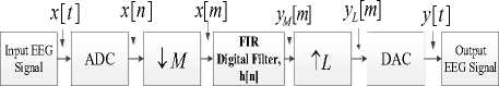
Fig.3. Block diagram of proposed multi-rate system for Case II.
equation (2) for up sampling operation; where EEG signal is converted to binary by ADC and up sampled or interpolated by L which is also in binary. In this implementation , only the non zero valued samples are fetched and used in the computation of the output samples. We see that, at each sampling instant into FIR filter, we must first shift the data by one place, read and save the latest input sample, x[n] and compute the current output sample using the difference equation (2). We also used the difference equation (3) for the operation of down sampling by M and use DAC to get output y(t). For the case II, we just use reverse operation of L and M into the flow chart. That means for case II the downsamling process is done first, then the signal is filtered using FIR filter, and lastly the up-sampling process is done. For case III, the upsampling rate is not equal to down-sampling rate . In this case, when L>M, the total number of samples increases with a ration L/M. However the main signal shape and carried information doesn’t change. On the other hand, when M>L, the number of samples decreases with a ratio of M/L. The Analog to Digital conversion(ADC) and Digital to Analog conversion(DAC) are used to make continuous data to discrete form and make the discrete data back to the original continuous type data after total operation. This total procedure is tested with ALTERA Cyclone DE II Device.
A simple block diagram representation of the proposed multi-rate system is given in Fig. 3. In this case we have used the equation (1) and the output of the FIR filter with the decimator by M:
yM(m) = y(mM)
which on combining with equation leads to the decimator equation
Start
Insert a sample of EEG signal x[t] in delay line
ALTERA Cyclone DE II BOARD
y [ t ]
y M( m) = ^ ^1 (h(k)^(mM - k)) (6)
The interpolation equations are
y ( m) = ® h ( k)y M( m - k) (7)
m — k = 0, L, 2L ....
otherwise
ADC x[n] +
Insert a zero into delay line by L into, x[n]
L-1 zeroes inserted? No
Yes
DAC
y [ n ]
____ 4 _____
Reduce zero into delay line by M y [ n ]
Sum of products yL [ n ]
Yes
*(■ —^М-0,
Case III: In this case we used case I Fig. 1, where L ^ M.
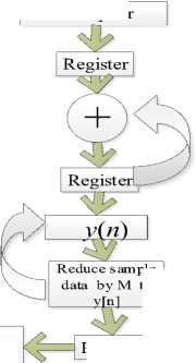
C. Flowchart of multi-rate system architecture
Fig. 4 shows a flowchart for the proposed multi-rate system operations for case I with interface ALTERA Cyclone DE II Device. Here we have used the difference
No
y [ m ] = ^ 1
N products summed ?
Compute product h [ k ] y [ m ]
Sum of products and load next sample into Register f
Fig.4. A simplified flowchart of proposed multi-rate system with interface ALTERA Cyclone DE II Board.
ADC, x[n]

Insert Up sample by L to x[n]
Data
Register

m emor y
h (0)
x ( n )
Coefficient
x ( n - N + 1)
memory
h ( N - 1)
Register

Register
Multiplier
DAC, x[t]
Register ple to
Fig.5. Pipeline MAC configuration of Proposed multi-rate system.
The pipeline registers serve as temporary store for coefficient and data sample pair. The product register also serves as a temporary store for the product. Fig. 5 shows a nonpipelined configuration for an arithmetic element for executing the equation (2) and (3)
-
a. The arithmetic operation of the proposed multi rate system is broken up into three distinct steps : memory read, multiply and accumulate .
-
b. Adds the previous product to the accumulator - initially, the product is zero .
-
c. EEG signal decimal data is converted by ADC and stored x [ n ] data into auxiliary register .
-
d. Increase the discrete samples data of x [ n ] by L ( Interpolator ) and stored L * x [ n ] data into auxiliary register .
-
e. The coefficients a k by the data memory x[n] accessed sequentially and applied to the multiplier . The products are summed in the accumulator and store into auxiliary register ( AR ). Initially AR point’s x[n] and then successively, points x[n — IV] decrement the address by 1 where we have used D flip flop for shift register operation for unit delay of samples .
-
f. Store up sampled filtered output y^n) into
register .
-
g. Decreasing the sampling rate of y k (n) by the
factor of M i.e. yA(n)/M and store it in the register .
-
h. Final discrete output y(n) and store into the register .
-
i. Apply y [ n ] into DAC and get the values of y ( t ).
-
D. Processing of Algorithm for proposed multi-rate system
For real time FIR filtering, the data x[n] and coefficients h[n] are stored in memory, conceptually. At first the date x[n] is increasing the sample by the factor L. If we consider EEG signal elements as illustrate follows are
x[n] = [1,2,3,4,5,6,7,8,9.....]
Up-sample by L=2 of x[n], it will happen as
x[n] = [1,0,2,0,3,0,4,0,5,0,6,0,7,0,8,0,9, ....]
These sequences are applied to FIR filter. To appreciate how the FIR filter works, consider the simple case of N=4, with the following differential equation by :
y(n) = h(0)x(n) + h(1)x(n — 1) +
h(2)x(n — 2)+) + h(3)x(n — 3)) + h(4)x(n — 4)
where x(n) represents the latest input sample, x(n — 1) the last sample, and x(n — 2) the sample before that.
Suppose the four-coefficients digital filter is fed from an ADC. The first thing to do is to allocate two sets of contigous memory locations (in RAM), one for storing the input data (x(n), x(n — 1),x(n — 2),x(n — 3), x(n — 4)) and the other for the filter coefficients (^(0), ^(1), ^(2), ^(4)) as depicted below:
Table 1. Coefficient values of biochip design
|
Data in RAM |
Coeeficients in Memory |
|
1 |
^(0) |
|
3 |
ед |
|
7 |
^(2) |
|
3 |
h(3) |
|
1 |
h(4) |
At initialization, the RAM locations where the data samples are to be stored are set to zero since always start with no data . The following operations are then performed:
-
• First sampling instant: To read data sample from the ADC and then up-sampled by L into x[n], shift data RAM one place (to make for the new data ), to save the new input sample , compute output sample from Equation (7) and then to send the computed output sample and the DAC before down-sample by M.
Table 2. First sampling instant values
|
Data in RAM |
Coefficients in Memory |
|
|
x(1) |
h(0) |
y(1) = h(0)x(1) + h(1)x(0) + h(2)x(-1) + h(3)x(-2) + h(4)x(-3) |
|
x(0) = 0 |
h(1) |
|
|
x(-1) = 0 |
h(2) |
|
|
x(-2) = 0 |
h(3) |
|
|
x(-3) = 0 |
h(4) |
-
• Second sampling instant: Repeat the above operation and work out sample and send to the DAC.
Table 3. Second sampling instant values
|
Data in RAM |
Coefficients in Memory |
|
|
x(2) |
h(0) |
y(2) = h(0)x(2) + h(1)x(1) + h(2)x(0) + h(3)x(-1) + h(4)x(-2) |
|
x(1) |
h(1) |
y(2) = h(0)x(2) + h(1)x(1) + h(2)x(0) |
|
x(0) = 0 |
h(2) |
|
|
x(-1) = 0 |
h(3) |
|
|
x(-2) = 0 |
h(4) |
• nth sampling instant: Repeat the above operation and work out sample and send to the DAC.
Table 4. nth sampling instant values
|
Data in RAM |
Coefficients in Memory |
|
|
x(5) |
h(0) |
y(n) = h(0)x(n) + h(1)x(n - 1) + h(2)x(n - 2) + h(3)x(n - 3) + h(4)x(n - 4) |
|
x(4) |
h(1) |
|
|
x(3) |
h(2) |
|
|
x(2) |
h(3) |
|
|
x(1) |
h(4) |
-
III. Experimental Results Anlysis
The methodology describes above sections which are implemented by The ALTRA DE2 Quartus II software which supports devices family Cyclone II FPGA Kit and also the Xilinx ISE 4.7 design suite. By implementing the processes, the main working procedures for Biochip are: find out the flowchart simulation of biochip, analyze the RTL block diagram, timing diagram and find out its operating parameters. Finally, the results will show best case of biochip design on multi-rate system.
The flowchart has been described in section II (C) for the case I. There are three parts which are up-sampling, FIR filter design and down-sampling process. All these processes are described in below sections.
-
i) Up-sampling:
The Fig. 6 illustrates the flowchart of the up-sampling process was used in all cases. We have used the raw EEG data that was described in section II. The simulation program has considered few parameters data_in as input of original EEG signal x[n], data_out1 as x[m]. It has been considered the data_in and the data_out1 as the 8-bit registers. The main motto in this operation is to increase the sampling rate of signal. For example, if the sequences of the samples of EEG signal are like (56,65,89,77,14,12......) then the resulting sequences of samples are like (56,0,65,0,89,0,77,0,14,0,12,0......) for
L=2. The data_out1 is assigned as the up-sampled values x[m] which is stored in 8 bit register.
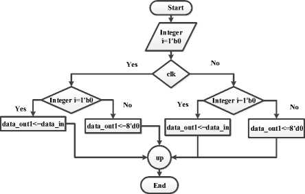
Fig. 6. Flowchart of the up-sampling process using Xilinx/ ALTRA DE2 Quartus II software.
ii) FIR filter design in FPGA
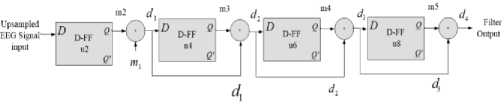
Fig.7. Basic diagram of designed FIR filter operations.
Fig. 7 illustrates the basic block diagram of the designed FIR filter. In this block, we have used four D flip flops for 4-unit delay operations. At first, the input is used up-sampled values x[m] which was stored into register. These up-sampled values are process with following procedures as described below. The EEG data signals which are up sampled are the direct input considered as m1.
-
• The 2nd D flip flops input is d 1 = { m 2 (output of the 1st D flip flop) + m 1 }
Output = m3
-
• The 3rd D flip flops input is d 2 = { d 1 ( m 1 + m 2 ) + m 3 (output of the2nd D flip flop)}
A. Flowchart and Algorithm
Output = m 4
-
• The 4th D flip flops input is d 3 = { m 4 (output of the 3 rd D flip flop) + d 2 }
Output = m s
-
• The final output = d4 = { m 5 (output of the 4th D flip flop) + d g }
-
iii) Down-sampling:
Fig. 8 shows the flowchart of the down-sampling process was used in all cases. It has been considered two parameters such as Filter_out as output of filter operation, we applied down or up-sampling operations by the parameter data_out2, y[m] in block diagram. These data are stored in 8-bit registers. The main aim is to decrease the sampling rate of the filtered signal. For example, if the sequences of the samples of EEG signal are like (22,19,28,16,29,12……) then the resulting sequences of samples are like (22,28,29…...) for M=2. The data_out2 is assigned as the down-sampled data which is stored in another 8 bit register.
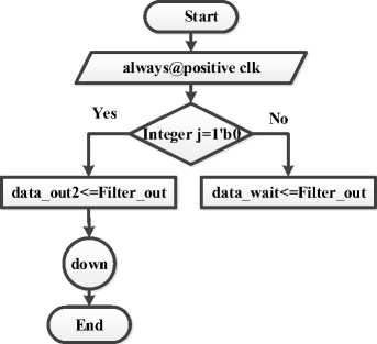
Fig. 8. Flowchart of the down-sampling process using Xilinx/ ALTRA DE2 Quartus II software.
-
B. RTL diagram of Biochip design
In the initial stage, registers have been used to perform up-sampling operations. For every clock pulse, an input data has been taken and the input is stored in an intermediate register. Data containing zero value is inserted into register within the next clock pulse. The Section-1 (circled) of Fig. 9 shows the up-sampler connection of RTL block. Furthermore, for FIR filter operation, we have used D flip-flops as memory element and it has connected four D Flip-flops in series in order to obtain the Shift Register operation where input clock and reset value controls the D flip-flops. Section-2 (rectangle) of Fig. 9 shows the RTL diagram of FIR filter. Finally, The Down-sampling operation is performed by again using registers. Section-3(circled) of Fig. 9 shows the down-sampling operation section. In the total RTL block, multiplexers (MUX 2:1) and Lookup tables( 4-LUT) have been used to generate logic operations. Here, registers have been used to store each and every data. Again, multipliers, 8-bit adders, latches are used in the RTL diagram as shown in Table 5 below.Next, Table 6 shows that the core temperature was 27.1° C during the simulation process. Table 6 also shows the voltage supply(Vcc), total current and total power needed for the proposed biochip design.
Table 5.HDL Synthesis Report (Macro Statistics) of Biochip design
|
Multipliers |
3 |
|
8x2-bit multiplier |
2 |
|
8x3-bit multiplier |
1 |
|
Adders/Subtractors (8-bit adder) |
4 |
|
Registers (D Flip-Flops) |
32 |
|
Latches (8-bit latch) |
1 |
|
IOs |
33 |
|
Total no. of paths |
32 |
Table 6. Power analyzer report of biochip design
|
Core temp. |
27.1 ° C |
|
Voltage supply(v cc ) |
2.5V |
|
Total Current (A) |
0.018A |
|
Total Power(W) |
0.081W |
C. Timing diagram of Biochip
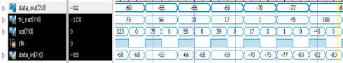
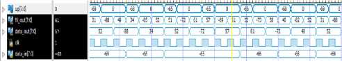
The timing diagram of Fig. 10 illustrates different cases. The Fig. 10 (a) shows the case I where we have used L=2 and M=2. In this case I we have mentioned the result parameters in Fig. 10(a) that we have simulated in our proposed Biochip design operations. The data input
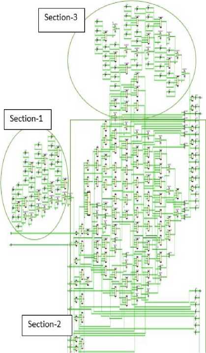
Fig.9. RTL diagram for Biochip design.
as x[n=0] indicted as well as data upsampled by L=2 between input data x L(1) (m = 0) = -69 up-sampled data as x L(2) (m = 0) = 0 within the single clock pulse. The filtered output data shows with respsect to input data xL (1) (m = 0) = -69 , the filtered output up-sampled data yL (1) (m = 0) = 52 and for up-sampled data x L(2) (m = 0) = 0 shows yL ( 2 ) (m = 0) = 84 within the same single clock pulse. The final filter out shown after down-sampling operation by M=2 which shows as ym(m = 0) = 84 after one clock pulse shift. The Fig. 10 (b) shows for the case I same operation for upsampling by L=3 and down sampling by M=3 where designed FIR operation carried out as described at section III (A) (ii). Fig. 10 (c) & (d) shows timing diagram for case II (M=2,L=2) and case III (L=3, M=2) respectively.
The Table 7 shows the timing summery of proposed biochip design on multi-rate system for the case I.
x L (1) ( m = 0) y L (2) ( m = 0)
y L (1) ( m = 0) x L (2) ( m = 0) y ( m = 0)
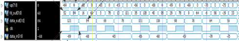
x ( n = 0)
Signle Clock Puls
a). Timing diagram for case I (L=2, M=2)
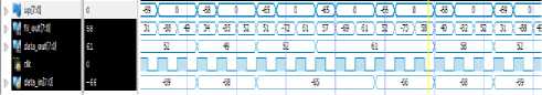
b). Timing diagram for case I (L=3, M=3)
c). Timing diagram for case II (M=2, L=2)
d). Timing diagram for case III (L=3, M=2)
Fig. 10. Timing diagram of proposed Biochip.
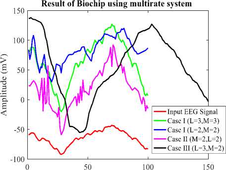
data and Output EEG data is shown in Fig. 11. It is clear that data have been filtered by huge ampifification.
The Fig. 11 illustrates a plot of the EEG datas and its final outputs of biochip design in multi-rate system. In this Fig. the raw EEG signal shows as red color, green and blue color shows for the case I where L=3,M=3 and L=2,M=2 respectively, magenta color for case II (M=2, L=2), black color shows for case III (L=3, M=2). Its clearly obeserved that sampling rate conversion has worked properly in this proposed system. The results of case I has shown better results than other cases. The case I have shown two different up-sampling and downsampling value such L=3, M=3 and L=2, M=2. It is clear that higher up-sampling and down-sampling rate works better. Case I and II have shown different way of multirate operations in proposed system design. The results of case I show better results than case II where case I uses up-sampling first and then down-sampling, case II uses down-sampling first and then up-sampling. Case III have shown sample values of EEG data increses than input EEG signal because of using the ratio L/M.
Table 7. Timing Summary of biochip design
|
Clock period |
1.656 ns |
|
Clock Frequency |
603.865 MHz |
|
Minimum input arrival time before clock |
10.744 ns |
|
Maximum output required time after clock |
15.369 ns |
|
Maximum combinational path delay |
14.155 ns |
D. Result Analysis
Sample Index [n]
Fig.11. Result Comparison of Input and output EEG signals.
Table 8. First 10 data for L=2 and M=2 case
|
Serial No. |
Data_in |
Up-sampled value |
FIR output |
Down-sampled value/ Data_out |
|
1 |
-69 |
-69 |
84 |
84 |
|
0 |
16 |
|||
|
2 |
-68 |
-68 |
68 |
68 |
|
0 |
3 |
|||
|
3 |
-65 |
-65 |
78 |
78 |
|
0 |
13 |
|||
|
4 |
-65 |
-65 |
101 |
101 |
|
0 |
35 |
|||
|
5 |
-66 |
-66 |
108 |
108 |
|
0 |
40 |
|||
|
6 |
-68 |
-68 |
98 |
98 |
|
0 |
29 |
|||
|
7 |
-69 |
-69 |
78 |
78 |
|
0 |
9 |
|||
|
8 |
-69 |
-69 |
64 |
64 |
|
0 |
-6 |
|||
|
9 |
-70 |
-70 |
56 |
56 |
|
0 |
-19 |
|||
|
10 |
-75 |
-75 |
33 |
33 |
|
0 |
-44 |
Coefficient Data memory memory
h [ N ] x ( n - N + 1)
h [0] x ( n )
MultiplierAccumulator
X Multiplier Y
∑
Register
Data Bus
Coefficients bus
Fig.12. Architecture of a hardware biochip design on multi - rate system for case I .
-
IV. Conclusion
We have presented an easy and simple approach biochip design based on multirtate system for EEG signal on FPGA Device. In this system, considered three cases for justification of best multi-rate based approach of the proposed system. We have also checked the system characteristics such as performance parameters: speed, clock frequecny, power consumpsion on HDL systhesis report, power analysis and timing diagram. In the future, this model can be enhanced and cope with larger dataset and fabciate of biochip, to apply into patient monitoring system. So it will be interesting to see how medical techonolgy is simple and fast way to diagonosis into patient monitoring system.
References Bio-chip design using multi-rate system for EEG signal on FPGA
- E. Niedermeyer, F. H. Lopes da Silva, “Electroencephalography: Basic Principles, Clinical Applications, and Related Fields” Lippincott Williams & Wilkins, 2005 Fifth edition.
- A.Mouraux , G. D. Ineetti “Across-trial averaging of event-related EEG responses and beyond,” Magnetic Resonance Imaging, September 2008, Volume 26, Issue 7, pp. 1041-1054
- M. Teplan “Fundamentals of EEG measurement,” Measurement Science Review, Volume 2, Section 2, 2002, pp.1-11.
- V. Sakkalis, T. Oikonomou, E. Pachou, I. Tollis, S. Micheloyannis and M. Zervakis, "Time-significant Wavelet Coherence for the Evaluation of Schizophrenic Brain Activity using a Graph theory approach," 2006 International Conference of the IEEE Engineering in Medicine and Biology Society, New York, NY, 2006, pp. 4265-4268.
- L. Milic, “Multi-rate Filtering for Digital Signal Processing: MATLAB Applications” Publisher: Information Science Reference; 1st edition December 26, 2008.
- Emmanuel Ifeachor. and Barrie WQ. Jervis, “Digital Signal Processing: A Practical Approach, 2/E” Publisher,” Pearson Education India, 2002, ISBN 813708241, 9788131708248.
- Chi-Jui Chou, Satish Mohanakrishnan, and Joseph B. Evans, “FPGA Implementation of Digital Filters”, Proc. Int. Conf. Signal Proc. Appl. & Tech. (ICSPAT’93), 1993.
- J. B. Evans, "Efficient FIR filter architectures suitable for FPGA implementation," in IEEE Transactions on Circuits and Systems II: Analog and Digital Signal Processing, vol. 41, no. 7, pp. 490-493, Jul 1994.
- S. M. Rabiul Islam, R. Sarker, S. Saha and A. F. M. Nokib Uddin, "Design of a programmable digital IIR filter based on FPGA," 2012 International Conference on Informatics, Electronics & Vision (ICIEV), Dhaka, 2012, pp. 716-721.
- S. M. R. Islam, R. Sarker and M. S. Monsur Hossain, "Design a digital system for detection of abnormality condition of heart from ECG waveforms," 14th International Conference on Computer and Information Technology (ICCIT 2011), Dhaka, 2011, pp. 24-29.
- S. M. R. Islam, S. Saha, M I. Khan “FPGA Based Digital System for Detection of Dicrotic Notch in the Carotid Pulse Signal” International Journal of Information and Communication Technology Research, Vol.2 No.12, pp. 872-880, December 2012.
- S. M. Rabiul Islam, A. F. M. N. Uddin, M. B. Hossain, M. I. Khan “FPGA based Heart Arrhythmia’s Detection Algorithm” ACEEE International Journal of Information Technology ,Vol. 3, No. 1, pp. 9-14, March 2013.
- G. Goslin. “A Guide to Using FPGAs for Application-Specific Digital Signal Processing Performance.” Xilinx Inc.
- Aggarwal, A. "FIR Filter Designing using XIllinx System Generator" International Journal of Computer Applications , Volume 68- No.11, , April 2013, pp. 37-41.
- Bhagyalakshmi.N., M. "Modified DA based FIR Filter in Multi-rate DSP systems on FPGA," International Journal on Recent and Innovation Trends in Computing and Communication, Volume 4, Issue 5, May 2016, pp.474-478.
- Sanada, Y., Ohira, T. & Chikuda, S., Igarashi, M., Ikebe, M., Asai, T., Motomura, M. "FPGA Implementation of Single-Image Super-Resolution Based on Frame-Bufferless Box Filtering," Journal of Signal Processing. 17. 111-114. 10.2299/jsp.17.111, 2013.
- Shenoi, B. “Introduction to Digital Signal Processing and Filter Design” John Wiley & Sons, Inc. 2006, ISBN: 978-0-471-46482-2.
- Sovili, P. " FPGA based model of processing EEG signal," Telekonmikacioni forum TELFOR. Srbija, Beograd, pp. 677-680, Novembar 24.-26., 2009.
- K. Sundaram, Marichamy and Pradeepa, "FPGA based filters for EEG pre-processing," 2016 Second International Conference on Science Technology Engineering and Management (ICONSTEM), Chennai, 2016, pp. 572-576.
- Wei-Chung Huang, Shao-Hang Hung, Jen-Feng Chung, Meng-Hsiu Chang, Lan-Da Van and Chin-Teng Lin, "FPGA implementation of 4-channel ICA for on-line EEG signal separation," 2008 IEEE Biomedical Circuits and Systems Conference, Baltimore, MD, 2008, pp. 65-68.
