Bit Serial Architecture for Variable Block Size Motion Estimation

Author: Krishna Kaveri Devarinti, T.Sai Lokesh, Gangadhar Vukkesala
Journal: International Journal of Image, Graphics and Signal Processing(IJIGSP) @ijigsp
Article in issue: 8 vol.5, 2013.
Free access
H.264/AVC is the latest video coding standard adopting variable block size, quarter-pixel accuracy and motion vector prediction and multi-reference frames for motion estimations. These new features result in higher computation requirements than that for previous coding standards.The computational complexity of motion estimation is about 60% in the H.264/AVC encoder. In this paper most significant bit (MSB first) arithmetic based bit serial Variable Block Size Motion Estimation (VBSME) hardware architecture is proposed. MSB first bit serial architecture main feature is, its early termination SAD computation compared to normal bit serial architectures. With this early termination technique, number computations are reduced drastically. Hence power consumption is also less compared to parallel architectures. An efficient bit serial processing element is proposed and developed 2D architecture for processing of 4x4 block in parallel .Inter connect structure is developed in such way that data reusability is achieved between PEs. Two types of adder trees are employed for variable block size SAD calculation with less number of adders. The proposed architecture can generate up to 41 motion vectors (MVs) for each macroblock. The inter connection complexity between PEs reduced drastically compared to parallel architectures. The architecture supports processing of SDTV (640x480) with 30fps at 172.8 MHz for search range [+8, -7]. We could reduce 14% of computations by using early termination technique.
Motion estimation, H.264, SAD, Macroblock, PE, Bit serial, variable block size, MV
Short address: https://sciup.org/15013023
IDR: 15013023
Text of the scientific article Bit Serial Architecture for Variable Block Size Motion Estimation
Published Online June 2013 in MECS
Variable Block Size Motion Estimation (VBSME) is one of the crucial features of video coding standard H.264/AVC [1]. Higher coding accuracy can be achieved with H.264/AVC by using smaller blocks and with the flexibility of VBS (Variable Block Size). However the computational cost of Motion Estimation (ME) is very high in real time operation, more efficient coding method is needed for high performance, low computational complexity.
For motion estimation process, each frame is divided into fixed number of non overlapping macro blocks. And each macro block is further divided into different sized blocks. The H.264 supports 7 different sub block sizes include 4x4, 4x8, 8x4, 8x8, 8x16, 16x8 and 16x16 pixels for VBSME. A hardware architecture that supports such scheme and provides respective motion vectors (MVs) need to be developed. SAD is the better block distortion method to use. The better way of performing VBSME is to get all small block sized SADs (4x4), merge them to get different sized SADs and compare them with previous measures to get respective minimum SADs and MVs. SAD for ME is shown in Equation (1).
N -1 N
SAD( vx, yx ) = E E | C ( m,n ) - R ( m + V x , n + V y )| (1) m =0 n =1
-p < Vx,Vy < p-1
MV = { ( V x , V y ) : SAD ( V x , V y ) = min e V x , V y ) ( SAD ( V x , V y ) ) } (3)
Where C is the current macroblock (CMB), R is reference block (RB), (i, j) is the pixel position, AD is the absolute difference at pixel position (i, j) and the size of macro block is NxN.
Motion estimation can be performed in either bit serial or parallel manner. We can say that bit parallel architectures operate on all the 8-bits (pixel value) at a time and bit serial architecture performs 1 bit at a time. Normal bit parallel architectures perform comparison operation after calculating total SAD. Bit serial architecture can terminate calculating SAD at the most significant bit (MSB) itself using sign digit comparator (if necessary). The comparison starts with MSB first manner. As all the operations are performed on MSB first manner, the early termination is possible in bit serial architectures. Early termination initiates new search position earlier and eliminates unnecessary SAD calculations. The resultant minimum SAD stores in bit by bit manner and simultaneously compared with the new SAD. If it is detected that at any position the new SAD is greater, the circuit stops the SAD calculation at that point and go for the next search point. Otherwise, the process continuous till the least significant bit (LSB) and stores the current SAD as minimum. The bit serial architecture has less internal bandwidth i.e.1/7 th of parallel architectures. As the bit serial architectures lacks the data reuse property they have large memory access and parallel architectures lacks the utilization of early termination and so have more computational cost.
We propose a modified bit serial architecture which supports early termination technique of normal bit serial architecture and data reusability of bit parallel architecture so as to get better performance. We designed a bit serial PE which supports both the data reusability and early termination.
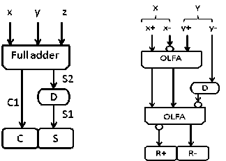
The PE we designed operates at 16 bits/cycle (16 pixel’s MSB to LSB) and is responsible for the calculation of SAD in MSB first manner. The PE can shift the data bit by bit to the neighboring PEs in three directions “bottom to top”, “left to right” and “right to left”. PE is combination of absolute (AB), online carry save adder (OLCSA), online sign digit adder (OLSDA), minimum SAD storing and online comparator (OLCOMP). The AB unit is for separating greater/lesser pixel values so as to eliminate the absolute operation in the process. We used MSB first sign digit adder (OLSDA – figure 1(b)) and MSB first full adder (OLFA – figure 1(a)) for the bit serial (radix-2) subtraction and addition operations respectively. We used an MSB first online comparator (OLCOMP) for early termination of SAD without any delay. We developed two types of variable block size adders (VBSAs) for different block size SADs by accumulating 4x4 SADs.
In section 2 we discuss about the 2D bit serial architecture for VBSME and illustrate the full search based motion estimation. Section 3 describes the new bit serial 2D architecture for VBSME. Section 4 describes the comparisons of proposed bit serial architecture with existing architectures. Section 5 gives the conclusions and the future scope of this work.
-
II. MSB first arithmetic
For discussing the bit serial architecture we need to know the basics of MSB first arithmetic. So, we discuss MSB first arithmetic then we go for the 2D bit serial PE structure.
MSB first adder and subtractor
The carry propagation latency is main problem with conventional LSB first adders. This problem is addressed and eliminated in MSB first arithmetic. MSB first arithmetic works with redundant number system (Table 2). The absolute operation is carried out by swapping the pixel values. We used OLSDA and OLFA for calculating sum of differences in MSB first manner. The functional block diagrams for these primitives are shown in figure 1. The OLFA has a normal full adder and a delay element. It gives the addition result in carry save manner. The OLSDA has two OLFAs including a delay element. The delay element used for synchronization between sum and carry bits. An example for OLFA is shown in table (1). We can see in the cycle 9, ‘0’s padded to inputs X, Y and Z. Bold 0s show the requirement to compensate the online delay introduced by the MSB-first arithmetic. We need to be more cautious in giving the ‘0’ padding. As in the very first cycle OLFA give garbage value due to the delay element in it. So, at the 9th cycle we need ‘0’ padding. The OLSDA can add two sign digit numbers. It gives result with two cycles of delay as it has two levels of delay elements. We use radix-2 Avizienis sign digit number system for MSB first arithmetic. Here each digit is represented with two bits as shown in table 2. We can observe the redundancy in representing ‘0’.
We rewrite the equation for SAD as shown in (6). Here, AD is the absolute difference between current and reference pixel locations at (i, j) and k is the bit position in the pixel value.
AD ( i, j ) = CMB ( i, j ) - RMB ( i + m , j + n )| (4)
= E kk =72 k x ( CMB ( i , j , k) - RB ( i + m, j + n , k )) (5) SAD ( v x , v y ) = E E E N 01 AD i, j (6)
The CMB value and RB value can be treated as positive and negative respectively for the SAD calculation. SAD always gives positive value as we have done absolute operation (AB) before addition.
Table1. Online full adder example: X=00101100 2 (44 10 ), Y=01100111 2 (103 10 ), Z=00100011 2 (35 10 ). Result [C+S] = 10110110 2 (182 10 ).
|
Cycle |
X |
Y |
Z |
C1 |
s2 |
S1 |
C |
S |
|
1 |
0 |
0 |
0 |
0 |
0 |
0 |
- |
- |
|
2 |
0 |
1 |
0 |
0 |
1 |
0 |
0 |
0 |
|
3 |
1 |
1 |
1 |
1 |
1 |
1 |
1 |
1 |
|
4 |
0 |
0 |
0 |
0 |
0 |
1 |
0 |
1 |
|
5 |
1 |
0 |
0 |
0 |
1 |
0 |
0 |
0 |
|
6 |
1 |
1 |
0 |
1 |
0 |
1 |
1 |
1 |
|
7 |
0 |
1 |
1 |
1 |
0 |
0 |
1 |
0 |
|
8 |
0 |
1 |
1 |
1 |
0 |
0 |
1 |
0 |
|
9 |
0 |
0 |
0 |
0 |
0 |
0 |
0 |
0 |
Table2. Radix-2 signed-digit system
|
Signed-digit value x i |
Digit representation (x i + , x i - ) |
|
+1 |
(1, 0) |
|
-1 |
(0, 1) |
|
0 |
(0, 0) |
|
0 |
(1, 1) |
(a) (b)
Figure1 (a) Online full adder (OLFA) (b) Online sign digit adder (OLSDA)
xl x2 x3 x4 x5 x6 x7 x8 x9 xlO xll xl2 xl3 x!4 x!5 xl6
-
III. modified bit serial architecture
We propose a 2D bit serial architecture which includes 16 PEs and two types of variable block size adders (VBSAs) elements. Each PE is to carry out the 4x4 SAD and the VBSA are meant for merging these 4x4 SAD to get variable size SADs (4x8, 8x4, 8x8, 8x16, 16x8 and 16x16 SAD).
-
A. Processing element (PE)
The processing element is composed of 16 AB units each having two registers (CR and SR) to store current and reference pixels, two OLFAs, one OLSDA, one minimum SAD block, one controller and a comparator as shown in figure 4. The PE is developed to shift data in three directions “from right to left”, “from left to right” and “bottom to top” to/from its adjacent PEs serially so as to support meander search pattern and to give 4x4 SAD. Every AB block decide the greater pixel and send that pixel bits (MSB first manner) to positive OLCSA tree and the lesser pixel bits to the negative OLCSA.
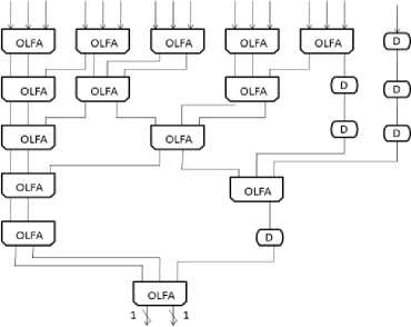
Figure2. Sixteen operands carry save adder
The sixteen operand OLCSA is implemented in 6 levels of OLFAs for addition of 16 bits in a cycle (figure 2). The delay (D) elements are included for synchronization of sum and carry bits. This block takes 12 cycles for adding 16 8-bit pixel values. This added result is accumulated in the OLSDA block to get the SAD. The OLSDA introduces two more cycles of delay as it has two levels of delay. It takes 13 cycles for completing 4x4 SAD calculation. The resultant SAD is compared with the minimum SAD stored in minimum SAD block. The minimum SAD block (two registers of 13 bits) stores the SAD in a sign digit representation form as shown in figure 3.The SAD calculation of further bits gets terminated by the controller if it is detected at any stage that the present SAD is greater. A signed digit (SD) comparator is employed for this purpose. The comparator we used here gives the result with no delay. In the best case: the MSB of current SAD is larger, which triggers the stop signal indicating an early termination since there is no need to process the remaining bits. In the worst case, the current SAD is less than the current minimum where we need to calculate SAD till LSB and that will be stored as the new current minimum.
Min SAD +ve
Min SAD -ve
Figure3. Minimum SAD storage registers
-
B. Variable Block Size Adder (VBSA)
Two types of VBSAs are introduced for calculating VBSME. VBSA1 (figure 5) is to compute 4x8, 8x4 and 8x8 SADs and VBSA2 is to process 8x16, 16x8 and 16x16 SADs. VBSA consists of one controller, five SDFAs, five comparators, five minimum SADs and one decoder. Three SDFAs are sufficient in VBSA to get 8x8 or 16x16 SAD. The controller detects all stop signals from comparators; give a termination signal so that the circuit starts with new search point.
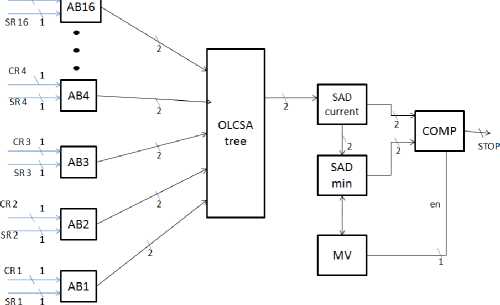
Figure4. The structure of 4x4 processing element (PE)
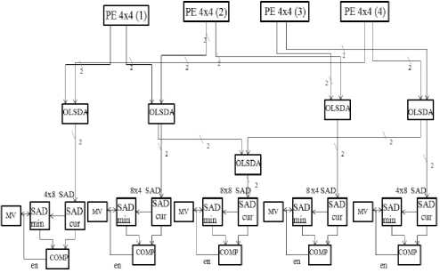
Figure5. Variable block size adder1 (VBSA1) to generate 4x8, 8x4 and 8x8 SADs.
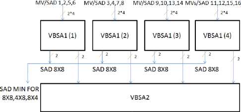
All the four VBSA1s calculate 8x8 SADs and give them serially to VBSA2 for getting 16x8, 8x16 and 16x16 SADs. Both VBSA1 and VBSA2 works similarly (figure (6))
parallel using 16 similar PEs in the architecture. They send those values to VBSA1. Four such VBSA1s (VBSA1 (1), (2), (3) and (4)) are employed for this purpose. PEs 1, 2, 5 and 6 give their results (4x4 SADs) to VBSA1 (1) and similarly PEs 11, 12, 15 and 16 give their SADs to VBSA1 (4) to give 8x4, 4x8 and 8x8 SADs. The VBSA1 takes 15 cycles to finish the 8x8 SAD calculations.
These four 8x8 SADs are sent to VBSA2 block to get 8x16, 16x8 and 16x16 SAD as shown in figure 7. The VBSA2 require 17 cycles for giving final 16x16 SAD. The Minimum SAD is in sign digit representation form and has different sizes in different levels of SADs. The comparator is also developed and controlled such that it can work properly for different levels of SADs.
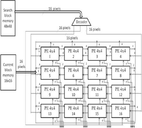
The PE requests memory to send next reference data through address generation unit (figure 8). The address generation unit knows the address of current pixels. The address generator generates an address of reference data for the memory unit with the help of controller information includes reference pixel location and load control signal.
-
D. Applying full search to the bit serial architecture
The proposed architecture supports Meander full search scan format. We illustrate the architecture flow in figure 8. After giving start signal to the circuit, in the first clock cycle the main memory fills the CR (current register) and SR (search register) of AB1, AB5, AB9 and AB13 (figure 4) with 8 bit pixels. These registers then shift the pixel values to the neighbor ABS units 2, 6, 10 and 14 in the next cycle. While this shift is occurring, the memory sends another set of pixels into registers of ABS units 1, 5, 9 and 13. This process continues for four cycles for filling the whole PE registers (Figure (10)).
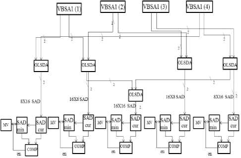
Figure6. Variable block size adder2 (VBSA2) to generate 8x16, 16x8 and 16x16 SADs.
C. Architecture Flow
We developed a 2D architecture based on PE and VBSAs. VBSME is achieved for full search algorithm with the proper interconnection of these blocks as shown in figure 7. The PE receives data from main memory through its input parallel ports. This PE is responsible for calculating 4x4 SAD. 16 such SADs are generated in
SAD MIN FOR 16X16,16X8,8X16
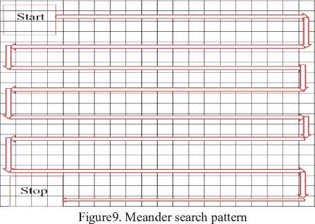
Figure7. Proposed architecture: composed of 16 PEs, four VBSA1 and one VBSA2.
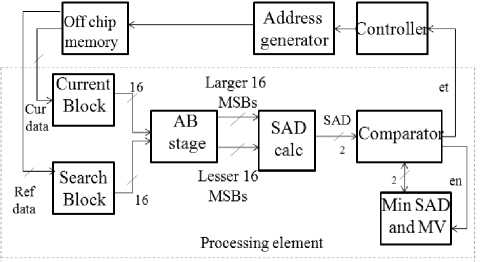
Figure8. The data flow of proposed architecture
From 5 th cycle onwards, all the AB units start giving out its pixel values (MSB to LSB). The bits of larger register to the positive OLCSA and the lesser register to the negative OLCSA block. Since the AB block decides which register is larger without any delay the OLCSA starts operating from 5 th clock. Because MSBs are already in use, the MSBs of SR of AB (1, 5, 9 and 13) blocks get overwritten with new pixel values. This shifting operation from MSB to LSB is done in pipelined manner (figure 10).
At the beginning of cycle 5, after loading the MSB bits of pixels to the OLCSAs, CR (current register) and SR (search register) registers of 1, 5, 9 and 13 shift their MSB bits to the registers 2, 6, 10 and 14, and the remaining registers shift their bits in a similar manner. In the next cycle all registers get updated and start new SAD computations. This way we achieve data reuse among the processing elements and pipelining to speed up the SAD computations.
The OLCSA tree takes 5 cycles of delay, OLSDA takes two cycles of delay to generate MSB pair of 4x4 SAD (in cycle 11). The VBSA1 and VBSA2 have 4 cycles of delay (two OLSDFA). So, the SD pair of SAD passes through VBSA1 in 15 th cycle and VBSA2 at the 18 th cycle.
Because of the pipelined architecture after 18 th clock cycle, every 17 clock cycles generates next set of 16x16 SAD bits.
The best case occurs when the MSB of new SAD is larger than the stored one after which the operation can be terminated (in cycle 19) and the worst occurs when the new SAD is smaller than the stored one where the decision made on the basis of LSB (in cycle 35).
Inside the PE or between PEs, the data is transmitted as bit by bit manner. As the search pattern applied is meander (snake type) figure 9, the circuit requires only 16 pixels (one row or column) for every new search point.
-
IV. PERFORMANCE ANANLYSIS
For a bit serial architecture, the early termination technique helps to reduce the number of SAD computations. And bit parallel architectures take the advantage of their 2D interconnect structure and highly pipelining structure to gain high performance. We have included both of these properties into our bit serial architecture. The performance of this architecture is shown in table 2.
Table3. Proposed bit serial VBSME circuit performance
|
Algorithm |
Meander Full search |
|
|
No. of PEs |
21 |
|
|
Block size |
4x4, 4x8, 8x4, 8x8, 8x16,16x8 and 16x16 |
|
|
Max. frequency (MHz) |
172.8 |
|
|
Search range |
32x32 |
16x16 |
|
Frame rate (fps) |
25 CIF |
57 CIF |
|
Cycles |
17663 |
4607 |
|
Memory (K bytes) |
20 |
8.4 |
|
Throughput (MB/sec) |
9926 |
37508 |
|
elk |
CR |
SR |
AB |
OLCSA |
4X4 SAD |
4X8 SAD |
8X8 SAD |
16X8 SAD |
16X16 SAD |
|
|
1 |
C7 |
R7 |
||||||||
|
2 |
C6 |
R6 |
||||||||
|
3 |
C5 |
R5 |
||||||||
|
4 |
C4 |
R4 |
||||||||
|
5 |
C3 |
R3 |
A7 |
|||||||
|
6 |
C2 |
R2 |
АБ |
|||||||
|
7 |
Cl |
Ri |
A5 |
|||||||
|
8 |
CO |
RO |
A4 |
|||||||
|
9 |
0 |
0 |
A3 |
Fil |
||||||
|
10 |
0 |
0 |
A2 |
F10 |
||||||
|
11 |
0 |
0 |
Al |
F9 |
S12 |
|||||
|
12 |
0 |
0 |
AO |
F8 |
SU |
|||||
|
13 |
0 |
0 |
0 |
F7 |
510 |
S13 |
||||
|
14 |
0 |
0 |
0 |
F6 |
S9 |
S12 |
||||
|
15 |
0 |
□ |
0 |
F5 |
S3 |
SU |
514 |
|||
|
16 |
0 |
0 |
0 |
F4 |
S7 |
S10 |
S13 |
|||
|
17 |
0 |
0 |
0 |
F3 |
S6 |
S9 |
S12 |
S15 |
||
|
18 |
C7 |
R7 |
0 |
F2 |
S5 |
S8 |
SU |
514 |
||
|
19 |
C6 |
R6 |
0 |
Fl |
S4 |
S7 |
S10 |
513 |
S16 |
|
|
20 |
C5 |
R5 |
0 |
FO |
S3 |
S6 |
S9 |
S12 |
S15 |
|
|
21 |
C4 |
R4 |
0 |
0 |
S2 |
55 |
SB |
SU |
S14 |
|
|
22 |
C3 |
R3 |
A7 |
0 |
SI |
S4 |
S7 |
510 |
513 |
|
|
23 |
C2 |
R2 |
A6 |
0 |
SO |
S3 |
S6 |
S9 |
S12 |
|
|
24 25 |
Cl |
RI |
A5 |
0 |
0 |
S2 |
S5 |
S3 |
SU |
|
|
co |
RO |
A4 |
0 |
0 |
SI |
54 |
57 |
510 |
||
|
26 |
0 |
0 |
A3 |
Fil |
0 |
SO |
S3 |
56 |
59 |
|
|
27 |
0 |
0 |
A2 |
F10 |
0 |
0 |
S2 |
55 |
58 |
|
|
28 |
0 |
0 |
Al |
F9 |
S12 |
0 |
SI |
S4 |
S7 |
|
|
29 |
0 |
0 |
0 |
F8 |
511 |
0 |
SO |
S3 |
56 |
|
|
30 |
0 |
□ |
0 |
F7 |
510 |
S13 |
0 |
S2 |
S5 |
|
|
31 |
0 |
0 |
0 |
F6 |
S9 |
S12 |
0 |
SI |
54 |
|
|
32 |
0 |
0 |
0 |
F5 |
S3 |
SU |
514 |
SO |
S3 |
|
|
33 34 |
0 |
0 |
0 |
F4 |
S7 |
S10 |
513 |
0 |
52 |
|
|
0 |
0 |
0 |
F3 |
S6 |
S9 |
S12 |
S15 |
SI |
||
|
35 |
C7 |
R7 |
0 |
F2 |
S5 |
S3 |
SU |
S14 |
SO |
Figure10. Timeline of proposed bit serial architecture for ME process.
Once all the values from memory have been input then the new data can immediately be input to each PE. This provides a continuous data transmission process that synchronizes with the data flow of image that exists in the PE. This means that each PE is 100% utilized.
We use CIF format for performance evaluation. For a search range of 32x32, a 16x16 macro block is compared with 1024 search blocks. The [3] and [5] reported the number of required clock cycles for a macro block as 16784 and 16384 respectively. For our architecture, by taking advantage of early termination, the best case get minimum SAD in the 19 th cycle and in worst case occurs at cycle 35. So, to produce a motion vector we need 1039*8=10472 cycles in best case and 1039*17=17663 cycles in worst case for search range of [-16, +15]. Similarly for search range [-8, +7], architecture takes 271*8=2168 cycles in best case and 271*17=4607 cycles in worst case to produce final motion vector.
The proposed bit serial 2D architecture effectively utilizes the computational resources. The architectures [3] and [4] utilize 256 PEs (each PE made to get the absolute difference of two pixels), [2] and [5] utilize 16 PEs of type 4 × 4 block size, and our bit serial architecture employs 21 processing elements out of which 16 of them are 4 × 4, 4 are 8 × 8 and 1 of at 16 × 16 granularity.
Kim et al. [2] employs an adder tree structure to compute larger SADs and is complex. In our architecture, we introduce a layer of processing elements and reduce the complexity of the adder tree structure. In [2], the adder tree has 8 adders for 4 × 8, and 8 adders for 8 × 4, where as in our architecture we use 2 adders per VBSA1, and a total of 8 adders to derive each 4 × 8 and 8 × 4 block. Similarly, [2] employs 2 adders for each 8 × 16 and 16 × 8 block, whereas in our architecture we used only 2 adders in VBSA2 to derive both 8 × 16 and 16 × 8 blocks. We use the same number of adders for VBSA2 to derive 8 × 8 and 16 × 16 blocks.
We used the shift registers for pipelining the data and these registers do not exist in parallel architectures like [2] and [5]. So, the processing speed of the circuit increases.
We compare the proposed architecture with other architectures in table 3 based on their clock rates and throughputs. All of these architectures are of search range (16x16). The proposed bit serial architecture is efficient in terms of throughput compared with other VBSME architectures.
Table4.Comparison with existing architectures
References Bit Serial Architecture for Variable Block Size Motion Estimation
- Wiegand, T., Sullivan, G. J., Bjontegaard, G., & Luthra, A. (2003). Overview of the H.264/AVC video coding standard. IEEE Transactions on Circuits and Systems for Video Technology, 13(7), 560–576.
- Kim, M., Hwang, I., & Chae, S. I. (2005). A fast VLSI architecture for full-search variable block size motion estimation in MPEG-4 AVC/H.264. In Proc. ASP-DAC (Vol. 1, pp. 631– 634).
- Yap, S. Y., & McCanny, J. V. (2004). A VLSI architecture for variable block size video motion estimation. IEEE Transactions on CAS II, 51(7), 384–389.
- Ou, C.-M., Le, C.-F., & Hwang, W.-J. (2005). An efficient VLSI architecture for H.264 variable block size motion estimation. IEEE Transaction on Consumer Electronics, 51(4), 1291–1299.
- Yap, S. Y., & McCanny, J. V. (2003). A VLSI architecture for advanced video coding motion estimation. In Proc. IEEE intl. conf. applications-specif ic systems, arch., processors (pp. 293–301).
- C. L. Su and C. W. Jen. Motion Estimation using MSD-first Processing. In Proc. of IEEE circuits, device and and systems, volume 150, pages 124–133, Apr. 2003.
- H. Loukil, F. Ghozzi, and A. Samet. Hardware implementation of Block Matching Algorithm with FPGA technology. In IEEE Int. Conf. on Microelectronics, volume 16, pages 542–546, 2004.
- M. Mohammadzadeh, M. Eshghi, and M. Azadfar. An Optimized Systolic Array Architecture for Full Search Block Matching Algorithm and its Implementation on FPGA chips. In IEEE Int. Conf. NEWCAS, volume 3, pages 327– 330, 2005.
- S.Wong, S. Vassiliadis, and S. Cotofana. A Sum of Absolute Differences Implementation in FPGA Hardware. In Proc. of 28th Euromico Conf., pages 183–188, Sept. 2002.
- C.Wei and M. Z. Gang. A novel SAD Computing Hardware Architecture for Variable-size Block Matching Estimation and Its Implementation with FPGA. In Proc. of IEEE Int. Symp. on Circuits and Systems, volume 1, pages 683–686, 2000.
- S. Lopez, F. Tobajas, A. Villar, V. de Armas, J. Lopez, and R. Sarmiento. Low Cost Efficient Architecture for H.264 Motion Estimation. In Proc. of IEEE Int. Symp. on Circuits and Systems, volume 1, pages 412–415, 2005.
