Conditions of a single-mode rib channel waveguide based on dielectric TiO2/SiO2

Author: Butt Muhammad Ali, Kozlova Elena Sergeevna, Khonina Svetlana Nikolaevna
Journal: Компьютерная оптика @computer-optics
Section: Opto-it
Article in issue: 4 т.41, 2017.
Free access
In this paper, we propose conditions for the design of a single-mode rib channel waveguide based on dielectric materials such as titanium dioxide (TiO2) and silicon dioxide (SiO2) for the 0.633-µm visible light. We also design Y-splitter structures, which show high-degree optical confinement and low bend losses at various radii of curvatures. Small radii of curvatures are extremely desirable in integrated photonics as they permit decreasing the dimensions but can also potentially reduce power consumption in the active devices.
Single mode, rib channel waveguide, titanium dioxide, silicon dioxide, beam propagation method
Short address: https://sciup.org/140228763
IDR: 140228763 | DOI: 10.18287/2412-6179-2017-41-4-494-498.
Text of the scientific article Conditions of a single-mode rib channel waveguide based on dielectric TiO2/SiO2
Optical communications through fiber have long been the technology of choice for high-speed long distance data links [1]. Progressively, as the capacity requirements have increased, the optical links have developed into shorter distance applications, such as fiber-to-the-home, local area network, and even into fiber optic interconnects between boards and cabinets. In the long run, optics would be used to interconnect the integrated circuits on a board or even to be used in intra-chip interconnects. That is, electrical interconnects, which have dominated since the infancy of electronics, are likely to be substituted with the optical interconnects in some cases [2]. Integrated optics devices are based on the processing of light confinement in optical structures called optical waveguides. It allows the confinement of light by total internal reflection, which takes place when the high index medium is surrounded by the low index medium [3–8]. The most significant passive elements in the integrated optics are the rib geometry waveguides [9–11]. They are the basic element practically in all integrated optical passive and active devices [9, 12].
In order to design a dielectric rib waveguides for optical communications, special care must be taken to confirm the single mode propagation of light for their farther coupling with the single mode fibres. One can subconsciously assume that the single mode condition for the rib waveguides have to look like the single mode condition for slab waveguides of the same dimensions, but it is not like this. The rib waveguide can be multimode in the vertical direction but if precise proportional sizes of the height and the width in thecen-tral region are chosen, it can support only one bound mode. In other words, all high order modes in the central rib region are filtered out by leaking away because their propagation constants are lower than that of the fundamental mode of the slab waveguide in the side region. Only the fundamental mode in the central rib region persists since only its propaga- tion constant is higher than that of the fundamental mode of the slab waveguide in the side region. Therefore, a criterion should be worked out for the proportional sizes of transversal dimensions in order to ensure the single mode propagation [13]. In this paper, conditions for single mode rib channel waveguide based on titanium dioxide and silicon dioxide are proposed; afterwards, the Y-splitter structure is also designed which shows the high degree of confinement and low bend losses even at low radii of curvature.
These kind waveguides consist of three layers of dielectric materials. Layer 1 has a thickness of H with a refractive index of n 1 . The layer is then etched while covering the rib section of the waveguide with the help of some metal mask; this gives rise to a slab of height h . Layer 1 has a refractive index of n 1 . Layer 2 and layer 3 have a semi-finite thickness and index of n 2 and n 3 , respectively. We shall assume that n 1 > n 2 and n 1 > n 3 . So that total internal reflection can occur at each interface. Layer 1 is referred to as the guiding layer, while layer 2 and 3 are a substrate and the cladding layer, respectively.
A guiding of this type can be formed simply by depositing a high index guiding layer onto a polished substrate. In our case, the cladding layer is air. Because of this geometry, it is normally described as an asymmetric rib waveguide and take n 1 > n 2 > n 3 . For the modeling of such waveguides, we proposed TiO 2 (2.5836 at 0.633 µm) and SiO 2 (1.4570 at 0.633 µm) as high and low refractive index materials, respectively. The refractive index difference between two material is quite high Δ n = 1.1266 which can be helpful in confining the light at the higher degrees of bends. The materials in which the guided light propagates must elude scattering and absorption losses in the wavelength range of interest [14].
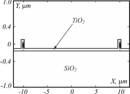
Fig. 1 shows the cross-sectional view of the rib waveguide, where h is the height of the slab, H is the slab height plus rib height and W is the width of the rib. The structuration of the layer can be done with different techniques [15].
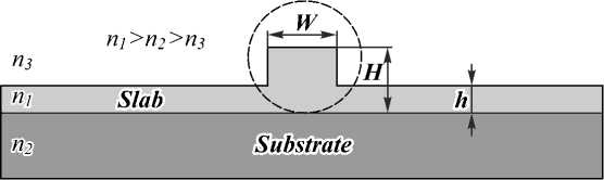
Fig. 1. A cross-sectional view of rib-waveguide
Conditions for single mode straight channel rib waveguide
Nowadays, an increasing number of optical modulators, filters and other functions relevant to telecommunication networks have been proposed as integrated or embedded in dielectric rib/ridge waveguides [16, 17]. Many of them share the widespread feature of being based on the propagation of the light beam inside a waveguide which has been designed to sustain only its fundamental mode of propagation to allow lower insertion losses when coupled to optical fibres. For the modeling of a single mode straight channel rib waveguide, the parameters such as h (height of slab), H (height of rib) and W (width of the rib) are considered. All the bounded modes are determined at 0.633 µm by using beam propagation method (BPM). The thickness of H is kept in the range of 100–1000 nm limited to the deposition techniques. Table 1, shows the parameters of waveguide used in the simulations and the type of waveguide obtained by it.
The ratios between ( h, H ) and ( W, H ) are plotted in Fig. 2 which represents the dimensions that can be used to design single and multi-mode rib channel waveguides. It can be seen that the region defined by the grey squares are the dimensions of waveguides that can only support a fundamental single mode and the region which is covered by black dots is useful to design multi-mode waveguides. Therefore, this graph can offer an approximation for indicating the dimensions of single mode waveguide based on these materials.
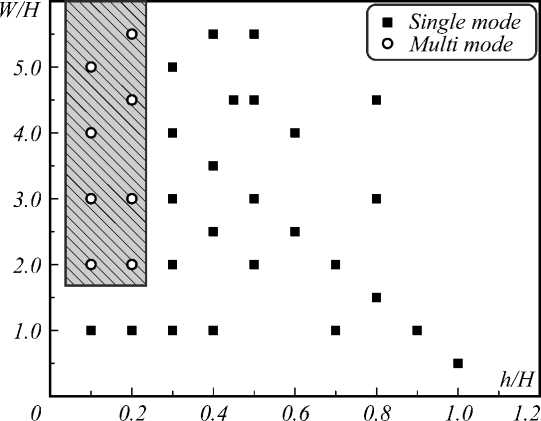
Fig. 2. Single and multi-mode waveguides dimensions at 0.633 µm. Grey and black points represent single and multi-modal waveguide dimensions respectively
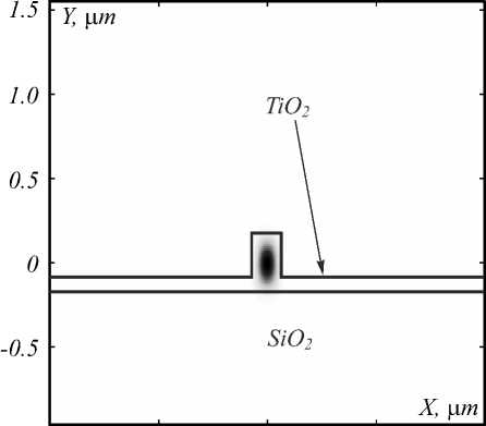
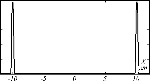
From Fig. 2, it is well noting that when the ratios of W/H >2 and h/H <0.3, the waveguide can support multimodes. Single mode waveguide dimensions are obtained when the ratios of h/H and W/H is greater than 0.3 and 1, respectively. However, when the ratio between h and H is higher than 1, then it is not possible to design a rib structure because the thickness of H should never be small than h. The simulated mode of a straight rib channel waveguide (Simulation number 5, Table 1) is shown in Fig. 3.
Table 1. Types of waveguides depending on its dimensions.
Where “h” is kept constant at 100 nm, however “H” and “W” are varied in each simulation
|
No. of Simul. |
h (nm) |
H (nm) |
W (nm) |
h/H |
W/H |
Waveguide type |
|
1 |
100 |
1000 |
5000 |
0.1 |
5 |
Multi |
|
2 |
100 |
500 |
2250 |
0.2 |
4.5 |
Multi |
|
3 |
100 |
300 |
1300 |
0.3 |
4 |
Single |
|
4 |
100 |
250 |
875 |
0.4 |
3.5 |
Single |
|
5 |
100 |
200 |
600 |
0.5 |
3 |
Single |
|
6 |
100 |
170 |
400 |
0.6 |
2.5 |
Single |
|
7 |
100 |
140 |
280 |
0.7 |
2 |
Single |
|
8 |
100 |
125 |
180 |
0.8 |
1.5 |
Single |
|
9 |
100 |
110 |
110 |
0.9 |
1 |
Single |
|
10 |
100 |
100 |
50 |
1 |
0.5 |
Single |
|
11 |
100 |
500 |
1000 |
0.2 |
2 |
Multi |
|
12 |
100 |
200 |
400 |
0.5 |
2 |
Single |
|
13 |
100 |
140 |
140 |
0.7 |
1 |
Single |
|
14 |
100 |
125 |
375 |
0.8 |
3 |
Single |
|
15 |
100 |
170 |
670 |
0.6 |
4 |
Single |
|
16 |
100 |
1000 |
3000 |
0.1 |
3 |
Multi |
|
17 |
100 |
1000 |
4000 |
0.1 |
4 |
Multi |
|
18 |
100 |
150 |
625 |
0.4 |
2.5 |
Single |
|
19 |
100 |
250 |
1375 |
0.4 |
5.5 |
Single |
|
20 |
100 |
200 |
1100 |
0.5 |
5.5 |
Single |
|
21 |
100 |
1000 |
1000 |
0.1 |
1 |
Single |
|
22 |
100 |
300 |
300 |
0.3 |
1 |
Single |
|
23 |
100 |
250 |
250 |
0.4 |
1 |
Single |
|
24 |
100 |
200 |
900 |
0.5 |
4.5 |
Single |
|
25 |
100 |
500 |
1500 |
0.2 |
3 |
Multi |
|
26 |
100 |
300 |
1600 |
0.3 |
5 |
Single |
|
27 |
100 |
125 |
560 |
0.8 |
4.5 |
Single |
|
28 |
100 |
1000 |
2000 |
0.1 |
2 |
Multi |
|
29 |
100 |
500 |
2750 |
0.2 |
5.5 |
Multi |
|
30 |
100 |
300 |
100 |
0.3 |
3 |
Single |
|
31 |
100 |
500 |
500 |
0.2 |
1 |
Single |
|
32 |
100 |
300 |
670 |
0.3 |
2 |
Single |
|
33 |
100 |
200 |
1000 |
0.45 |
4.5 |
Single |
1.0
-4-2 0 2 4
Fig. 3. Simulated single mode of a straight rib channel waveguide
0.8
0.6
0.4
0.2
О
Single mode Y-splitter structure
After proposing the conditions of straight rib channel waveguide, the design for the balanced Y-splitter structure is proposed. Several Y-splitter structures with varying radii of curvatures are simulated. The waveguide dimensions (Simulations: 1–6) are kept constant. The size of Y-splitter is fixed to 8 mm but with in- creasing radii of curvature in each simulation. The schematic of the Y-splitter design based on TiO2/SiO2 is shown in Fig. 4. The length of the input straight channel waveguide is kept as long as possible depending on the design. This helps in removing the fluctuations and clean the propagating mode.The detail about the parameters is shown in Table 2.
Table 2. Y-splitter structure of 8000 µm long with various radius of curvature
|
No. of simul. |
h (µm) |
H (µm) |
W (µm) |
Length of input straightwaveguide, L in (µm) |
Length of bend Waveguide, L bend, (µm) |
Length of output straight waveguide, L out (µm) |
Separation between two arms, L s (µm) |
Radii of curvature, R (mm) |
|
1 |
0.05 |
0.25 |
0.5 |
2000 |
1500 |
4500 |
2 |
560 |
|
2 |
0.05 |
0.25 |
0.5 |
2000 |
1500 |
4500 |
4 |
280 |
|
3 |
0.05 |
0.25 |
0.5 |
2000 |
1500 |
4500 |
6 |
188 |
|
4 |
0.05 |
0.25 |
0.5 |
2000 |
1500 |
4500 |
8 |
140 |
|
5 |
0.05 |
0.25 |
0.5 |
2000 |
1500 |
4500 |
10 |
110 |
|
6 |
0.05 |
0.25 |
0.5 |
2000 |
1500 |
4500 |
12 |
93 |
-----Simulation 1
Simulation 2
-----Simulation 3
-------Simulation 4
----Simulation 5
-------Simulation 6
Intensitv, a.u.
1.2 '
1.0
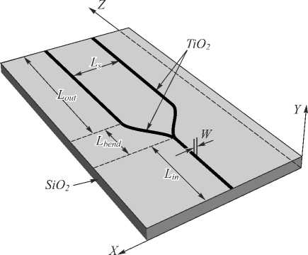
Fig. 4. Schematic of 8 mm long Y-splitter structure with varying distance between two arms ranges from 2–12 µm
0.8
0.6
0.4
0.2

Z, mm
a) О 1 2
Intensitv, a.u.
0.5 0Г"-----1—
7 8
0.49
0.48
The propagation of light intensity in one arm of 6 different Y-splitters with a varying radius of curvature, R is plotted in Fig. 5( a ). Since the Y-splitter structure is symmetric, therefore the power in each arm is equal. By keeping the optimum separations, coupling effect between two arms can be avoided. An optimum value of the radius of curvature should be selected in order to provide a smooth bending to the propagation light. S-bend waveguides with fixed radius of curvature R range between 93–560 mm are used to design the Y-splitters. S-bend waveguides are important as input/output waveguides for directional couplers and as waveguide path transformers in various circuits.
The fundamental mode of a straight channel rib waveguide was calculated and used as a launch field for Y-splitter. Let’s consider, the launch field has an intensity of 1 a.u. The Y-splitter with a separation of 10 µm between its arms contains the maximum energy of 0.491 a.u / arm. The lowest energy of 0.465 a.u/arm was obtained in the case of Y-splitter with 4 µm of separation between its arms. This shows an energy difference of nearly 3 % if Y-splitters are designed with R between 93– 560 mm as shown in Fg. 5( b ).
0.47
-----Simulation 1
Simulation 2
-----Simulation 3
-------Simulation 4
----Simulation 5
-------Simulation 6
0.46
0.45
b) 4.0 4.2 4.4 4.6 4.8
Z, mm
5.0
Fig. 5. Variation of launch power a) 8 mm long Y-splitter structure with varying distance between two arms ranges from 2–12 µm b) Magnified image of the power in the propagation length from 4–5 mm
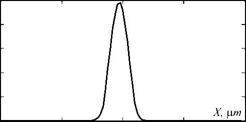
Out of six simulations shown in Fig. 5, we choose the best design of the Y-splitter and plotted its mode profile at the output as shown in Fig. 6( a ). The separation between the two arms was at 20 µm to avoid any possible evanescence field coupling between two arms. The optical field at the output of the matched S-bends and in the subsequent straight waveguide section is undistorted. As a consequence, the fields at the Y-branch output are balanced as demonstrated by the horizontal cross-section of the mode as shown in Fig. 6( b ). Moreover, there is no leakage of the mode in the substrate as can be seen in Fig. 6( c ), where mode has an FWHM of 0.1692 µm which is nearly equal to the height of the rib.
0.4
0.3
0.2
0.1
О
Intensity, а.и. 0.5 0.4 0.3 0.2 0.1
О b)
Intensity, а.и.
0.5
0.4
0.3
0.2
0.1
О
c) -1.0 -0.5 0 0.5 1.0
Fig. 6. Simulated results of a Y-splitter at 0.633 µm with a) Mode profile at the output of Y-splitter b) Horizontal cross-section profile of the mode c) Vertical cross-section of the mode
Conclusion
We proposed the conditions of a single mode rib channel waveguide based on TiO 2 and SiO 2 dielectric materials at 0.633 µm visible light by optimizing different parameters of the waveguide with the help of Beam Prop software. These dielectric materials have high refractive index contrast which makes them an outstanding platform for the realization of S-bend and Y-splitters with the small radii of curvature. Based on these results, many optical elements such as S-bend, Y-splitter can be realized which can be used for different optical applications. Moreover, the Y-splitter structures are designed which shows the high degree of optical confinement and low bend losses at various radii of curvatures. Small radii of curvatures are extremely desirable in integrated photonics as they permit decreasing the dimensions but can also potentially reduce the power consumption in the active devices.
References Conditions of a single-mode rib channel waveguide based on dielectric TiO2/SiO2
- Senior, J.M. Optical fiber communications: Principles and practice/Senior JM. -Pearson education Ltd., 2009. -1128 p. -ISBN: 978-0-13-032681-2.
- Tong, X.C. Advanced materials for integrated optical waveguides/X.C. Tong. -Switzerland: Springer International Publishing, 2014. -552 p. -ISBN 978-3-319-01549-1.
- Butt, M.A. Channel waveguides and mach-zehnder structures on RbTiOPO4 by Cs+ ion exchange/M.A. Butt, M.C. Pujol, R. Sole, A. Rodenas, G. Lifante, J.S. Wilkinson, M. Aguilo, F. Diaz//Optical Materials Express. -2015. -Vol. 5, Issue 5. -P. 1183-1194. - DOI: 10.1364/OME.5.001183
- Butt, M.A. Low-repitition rate femtosecond laser writing of optical waveguides in KTP crystals: analysis of anisotropic refractive index changes/M.A. Butt, H.D. Nguyen, A. Rodenas, C. Romero, P. Moreno, J.R. Vazuez de Aldana, M. Aguilo, R.M. Sole, M.C. Pujol, F. Diaz//Optics Express. -2015. -Vol. 23, Issue 12. -P. 15343-15355. - DOI: 10.1364/OE.23.015343
- Butt, M.A. Fabrication of Y-splitters and Mach-Zehnder structures on (Yb, Nb):RbTiOPO4/RbTiOPO4 Epitaxial layers by reactive ion etching/M.A. Butt, R. Sole, M.C. Pujol, A. Rodenas, G. Lifante, A. Choudhary, G.S. Murugan, D.P. Shepherd, J.S. Wilkinson, M. Aguilo, F. Diaz//Journal of Lightwave Technology. -2015. -Vol. 33, Issue 9. -P. 1863-1871.
- Kazanskiy, N.L. Optical nanoresonator in the ridge of photonic crystal waveguides crossing/N.L. Kazanskiy, P.G. Serafimovich, S.N. Khonina//Computer Optics. -2011. -Vol. 35(4). -P. 426-431. -.
- Strilets, T.S. Simulation of waveguide modes in multilayer structures/T.S. Strilets, V.V. Kotlyar, A.G. Nalimov//Computer Optics. -2010. -Vol. 34(4). -P. 487-493. -.
- Moiseeva, N.M. The calculation of eigenvalues modes of the planar anistropic waveguides for various angles the optical axis/N.M. Moiseeva//Computer Optics. -2013. -Vol. 37(1). -P. 13-18. -.
- Adams, M.J. An introduction to optical waveguides/M.J. Adams. -New York: John Wiley & Sons, 1981. -401 p. -ISBN: 978-0-471-27969-3.
- Rib waveguide theory by the spectral index method/Ed. by P.N. Robson, P.C. Kendall. -Research Studies Press Ltd., 1990. -200 p. -ISBN: 978-0471929239.
- Soref, R.A. Large single mode rib waveguides in GeSi-Si and Si-on-SiO2/R.A. Soref, J. Schmidtchen, K. Petermann//IEEE Journal of Quantum Electronics. -1991. -Vol. 27. -P. 1971-1974. - DOI: 10.1109/3.83406
- Wang, S. Principles of distributed feedback and distributed Bragg-reflector lasers/S. Wang//IEEE Journal of Quantum Electronics. -1974. -Vol. 10, Issue 4. -P. 413-427. - DOI: 10.1109/JQE.1974.1068152
- Pogossian, S.P. The single mode condition for semiconductor Rib waveguides with large cross section/S.P. Pogossian, L. Vescan, A. Vonsovici//Journal of Lightwave Technology. -1998. -Vol. 16, Issue 10. -P. 1851-1853. - DOI: 10.1109/50.721072
- Yeatman, E.M. Strip-loaded high confinement waveguides for photonic applications/E.M. Yeatman, K. Pita, M.M. Ahmad//Journal of Sol-Gel Science and Technology. -1998. -Vol. 13, Issue 1-3. -P. 517-521.
- Butt, M.A. Fabrication of optical waveguides in RbTiOPO4 single crystals by using different techniques/M.A. Butt, M.C. Pujol, R. Sole, A. Rodenas, G. Lifante, M. Aguilo, F. Diaz, S.N. Khonina, R.V. Skidanov, P. Verma//Proceedings of SPIE. -2016. -Vol. 9807. -98070C. - DOI: 10.1117/12.2231368
- Boudrioua, A. Photonic waveguides: Theory and applications/A. Boudrioua. -Hoboken, NJ: John Wliey & Sons, Inc., 2009. -320 p. -ISBN: 978-1-84821-027-1.
- Lifante, G. Integrated photonics: Fundamentals/G. Lifante. -Chichester: John Wiley & Sons Ltd., 2003. -198 p. -ISBN: 978-0-470-84868-5.
