Cost Modeling for SOC Modules Testing

Author: Balwinder Singh, Arun Khosla, Sukhleen B. Narang
Journal: International Journal of Information Engineering and Electronic Business(IJIEEB) @ijieeb
Article in issue: 2 vol.5, 2013.
Free access
The complexity of the system design is increasing very rapidly as the number of transistors on Integrated Circuits (IC) doubles as per Moore’s law. There is big challenge of testing this complex VLSI circuit, in which whole system is integrated into a single chip called System on Chip (SOC). Cost of testing the SOC is also increasing with complexity. Cost modeling plays a vital role in reduction of test cost and time to market. This paper includes the cost modeling of the SOC Module testing which contains both analog and digital modules. The various test cost parameters and equations are considered from the previous work. The mathematical relations are developed for cost modeling to test the SOC further cost modeling equations are modeled in Graphical User Interface (GUI) in MATLAB, which can be used as a cost estimation tool. A case study is done to calculate the cost of the SOC testing due to Logic Built in Self Test (LBIST) and Memory Built in Self Test (MBIST). VLSI Test engineers can take the benefits of such cost estimation tools for test planning.
Cost modeling, System on Chip, VLSI Testing, Cost Estimation Tool
Short address: https://sciup.org/15013172
IDR: 15013172
Text of the scientific article Cost Modeling for SOC Modules Testing
Published Online August 2013 in MECS (http://www.
The advancements in the fabrication techniques and equipments make it possible to integrate hundreds of thousands of transistors passive components and multiple stand-alone VLSI designs on a single chip to have full functionality for an application. With increasing computational demand from application side and deep sub micron semiconductor processing from technology side together make whole system into a single chip reality. The system knowledge and expertise brings hardware elements such as processors and controller along with the software components to a Single chip solution and is called System on Chip. In general, SOC design incorporates a programmable processor, on chip memory, audio and video controllers, modems, Internet-tuner, graphics controllers, DSP functions and accelerating functional units implemented in hardware. The required shift for SOC design depends on two industrial trends: the development of application-oriented IC integration platforms for rapid design of SOC devices and derivatives, and the wide availability of reusable virtual components. The performance of these systems reaches few gigahertz while the power consumption is of the order of milli Watts.
IP Core Design
IP Core Verification

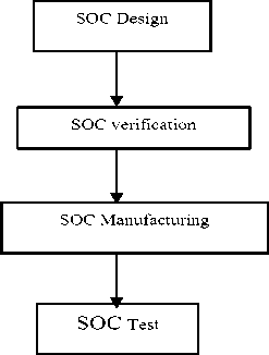
Figure 1: Single Stage System-on-chip test
After every three years, silicon complexity quadruples according to Moore’s law. This complexity accounts for the increasing size of cores and the shrinking geometry that makes it necessary to include more and more parameters in the design criterion. The design methodologies are improving day by day.
As SOC devices have grown from early discrete lumped designs to high levels of integration. Automatic Test Equipment (ATE) became the most suitable platform for testing complex SOC. This paradig m shift forced both ATE vendors and test engineers to broadly consider the test equipment setup that provides the maximum test coverage for a wide variety of SOC DUTs. Without using a Design for Testability (DFT), Test engineer spends more time on creating tests for ATE. DFT is the method used to combine the design and test logic together. It allows knowing about the IP core and internal scan chains. In ATE this information is typically hidden and also requires high volume of external memory to store the test vectors. The flow chart shown in figure 1 gives the detailed form of SOC manufacturing to SOC testing
To test system-chips adequately, test solutions need to be incorporated into individual cores and then the tests from individual cores need to be scheduled and assembled into a chip level test strategy. Each type of core has different test requirements.
Increasing integration scales, densities, performances, functionality, and decreasing sizes and power consumption, becomes the reason for the increase in the price to pay for the complex designs. To compensate these raised expenditures, the cost roughly translates into spending production time for a new design, or hiring more skilled designers.
Time-to-market can often outweigh design prototyping and product costs commercial product. To study the economic impact of delay of the product in market. ATE [1] has developed a delay model as discussed below. Considering the real-life competitiveness, the later a product arrives in the market, the lower are the revenues obtained from it.
Suppose the peak value of the market growth is Pmax and reached after time ‘T’. The revenue loss due to delay D can be calculated as: Area of outer triangle – Area of inner triangle.
Right time entry into market:
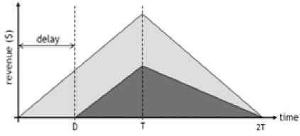
Figure 2: Consequences of time-to-market [14]
For Late entry
R * 7.T * P1
exp 2 lmax
R deiay =2 * (2T-D ((T - D )/T) * Pmax
R net R exp R delay
D (3T - D)
Rnet =
If the product arrives late in the market its life is short which results in high loss to the company.
As large number of parameters are merging to have more accuracy in complex designs, at the same time these design parameters are also forcing more complex testing parameters, which make testing a tedious job to handle with low power and lower cost at higher speed
-
II. RELATED WORK
Many researchers have explored the idea and benefits of the cost of manufacturing tests in the past. Some of them are discussed here. I. D. Dear et.al. [4] The authors discussed the economics of test. The EVEREST test strategy planner tool, which is used for the test planning. Andrew [5] developed a Semiconductor Test Economic Model that can easily be applied to lower the overall cost of test and improving throughput. It gives idea to the test engineers for better decisions on the issues related to: test time reduction, multisite testing, yield, handler index time, ATE Utilization, and ATE purchasing. Kenneth [6] gives the estimated economic benefits of the DFT and also suggested that testability features should not be added to complex or high volume products. Abadir et al. [7] developed Hi-TEA, a MCM testing strategy selection tool, which helps to select the cost effective test strategy for the multi-chip module (MCM). Their tool requires cost parameters such as die test cost and wafer yield, which are the parameters difficult to know in the early stages of design. Therefore, their tool may not be practical to predict a chip testing cost early. Karthik Sundararaman et. al[8] addresses the limitation of fault tolerance model by introducing the cost model for these by taking into account the reliability factor. Li-Rong Zheng [9] presents the review and analysis of cost performance trade-off system chip versus system on package. Methodology used is based on quantitatively analysis. Songjun Lee et. al [10] proposed the economic models to predict the total cost SOC development at the early design stage. Erik et.al [11] discussed the benefits and tradeoffs by applying the technical cost modeling on 4 applications. Sudarshan et al [12] proposed a correlation based signature analysis technique to sort out the limitations of measurement inaccuracies at wafer level testing. For this generic cost model is developed. Von-Kyoung Kim et. al.[18] proposed a test cost prediction model which estimates and optimize manufacturing test cost
-
III. COST MODELING FOR SOC MODULES TESTING
-
3.1. Design for Testability Modeling
A system consisting of Digital and Analog IP’s which are not identical are assumed in the present work. The proposed cost model consists of the main cost factors which are involved in the designing, manufacturing and testing of the system on chip. The cost includes the material, equipment, labour cost (NRE) and time. The design phase also includes the DFT modules to test the system with less use of ATE as ATE needs deeper access of the internal pins of each blocks which is not possible due to the complexities of the chip. DFT methods help to generate test patterns internally But DFT panelize the area overhead which are balanced by reducing test generation cost use of internal BIST etc. DFT impacts the design and its testability and also concentrates on manufacturability; yields test hardware and profitability factors. Manufacturing cost includes the mask generation cost, equipment cost, and throughput of the process, manpower and packaging cost. Manufacturing costs can be affected by test actions because of factors such as decrease in silicon yield. Test cost includes test generation, as well as cost of test IPs, ATE, Test programming, Labor cost and fault simulation.
We assume the system consist of n number of IP’s which are not identical. The proposed cost model consists of the main cost factors which are involved in the designing, manufacturing and testing of the system on chip. The cost includes the material, equipment, labor cost (NRE) and time. The design phase also includes the DFT modules to test the system with less use of ATE as ATE needs deeper access of the internal pins of each blocks which is not possible due to the complexities of the chip.
DFT techniques required more time during the design phase. Cost models give the pre-estimation about the cost and time. As discussed in previous section SOC consumes large number of complex IP modules and these modules must be designed for reuse in different devices .The use of DFT for the testing of these IPs affects the testing cost. DFT total cost consists of the direct cost i.e. area, test generation, test time, design efforts, test automation and infrastructure cost and indirect cost (meeting performance, activity coverage cost, diagnostic support etc.) In SOC with DFT feature, the cost is additive to the normal IC test cost.
Testing cost is computed as [13]
C_ test = C _ Fab + C _exess + C _ silicon
C fab
Q wafer
2 n P wafer R wafer
………………………………4
Q wafer : unit cost of the wafer
R wafer : wafer radius
Β wa f er percentage of wafer area that can be divided into dies
-
A: area of the die
-
Y: yield of the die
Silicon overhead cost is calculated for extra area required for DFT circuits. if we want to find the difference with DFT and without DFT it can be calculated as
C Q wafer _____ [ 7 dfT fab Qwafer R Wa f er Y D FT
—
aNo DFT ] yNo DFT^
Yield can be modeled using Seeds equation [4]
Y = ^~
1+AD
……………………………………………..6
A: area of the IP
D: defect density in IP
Area parameter is modeled for logic and memory part differently from above equation:
A loglc = (1 + Y area )7 .................................... 7
Y area= area overhead of DFT
_ / (1+(log 2 *Msize )1.33) \ A m e m or y = V Msize )...........................
-
3.2. Built in Self Test Modeling
BIST provides a potentially good solution to problems arising in SOC’s i.e. when IP cores are available from the different vendor’s for the SOC design and manufacturing. This includes core isolation, core access, test reuse, tester qualification etc. In this [12] gives the modeling of Logic BIST. We have modeled these equations in terms of cost. Firstly if development time is reduced due to LBIST, the Manpower cost is evaluated as [12]
C labor N E * C per person * T savingLBIST .................. 9
N E : Average Number of Persons involved in design
C p er p erson: average cost per person per day
T sav i n g : time saved by LBIST during the testing.
But it is not positive in ceasing of LBIST design. Cost due to area overhead can be calculated same as equation 3. BIST generates test patterns internally and Test some of the IP parts without extra pin in external circuits. So tester cost reduces to some extent and also the pin count and packaging cost also saves in this method.
Test cost is calculated as
C tester N v T, . [C t ext * T t C TextLBIST *
T tLBIST ]……………………………………………………10
C Text : price of external tester to Access the chip without LBIST
Tt: tester time without LBIST
CtextLBIST: cost of the external tester access the chip LBIST
T tLBIST : time of tester with LBIST
R d e p : annual depreciation rate of the tester.
Tsec i nyear : second in one year
-
3.3. Memory Built in Self Test Modeling
As we know that 90% of the chip area will be occupied by the memory as per International Technology Roadmap for Semiconductor 2009[1] . So it clearly indicates that more testing is required for memory, which also effects the cost of testing. Memory BIST plays an important role to control the test cost to some extent. The manpower cost is evaluated as [12]
NE: Average Number of Persons involved in design
C p er p erson: average cost per person per day
T saving: time saved by MBIST during the testing.
Cost due to area overhead can be calculated same as equation 8 and area associated with memory BIST can be calculated same as with equation 6. Cost benefits with use of MBIST and a logic tester is also used with memory tester so Cost of Memory tester can be calculated from the equation с. .
utester
T tMBisT
= Nv" I (C tM ext * T tM -
T Sec in year L
. Rdep "I
) T * C tM ext * T tLBi ST I
T Sec in year -I
C TextMBIST *
Where; T tMBIST amount of time the memory tester
T tLBIST amount of time the logic tester with MBIST
C textMBIST: cost of memory external tester
C tLBIST : logic tester
-
3.4. Production Testing Modeling
The main factor that affects the production testing is overall manufacturing test and test escape cost. The cost model allows the company to calibrate test processes to the risks of the product. The total production cost can be calculated from total manufacturing i.e. Cost of the testing the devices plus the cost of escape [11]
C Omt C mt + C tescape ....................................13
Comt : overall cost of manufacturing test C mt : the cost of the testing in manufacturing Ctest : cost of the test escape
C total = C omt * Volume....................................14
Test cost is the expenditure during the test execution for the chip. Chip testing is classified into two categories: one is at the wafer level in which each die of the chip is tested with help of ATE and faulty dies are marked with red ink. This faulty die does not package to save the cost of package. Another type of testing is done after the package. Total cost of testing depends upon the number of IP’s or functional blocks present in the SOC chip. The cost of ATE is added to another modules cost if they are presented in the IP’s.
y n
-
C total test cost ATE+ ^i=i C bist ........................ 15
ATE cost model As discussed in previous section DFT techniques for digital circuits bring the parallelism into the testing, it reduces the requirement of the ATE but on the SOC both analog and digital blocks are tested at same time and it has been also proven its effectiveness in[15]. The cost model benefit of the multisite is discussed in the [5]. The total ATE cost can be calculated by equation given below. It also includes the depreciation cost of test cell.
-
C ATE total C cap + C op + C Pc + C pkg ..................16
C ATE total: Total ATE cost
C cap: Capital cost of ATE
C op : operating cost
C pc : Probe card Cost
C pkg : Package cost
-
IV. COST MODELING TOOL WITH MATLAB GRAPHICAL USER INTERFACE
As mathematical equations are modeled in MATLAB for the various parameters calculation. A Graphical User Interface is required so that the designers and test engineers can do cost estimation easily. In this MATLAB (.fig file) is designed and backend callback functions are called from GUI for each calculation. Development of GUI and its link with the database are shown in figure 3. In this, GUI has been created for mathematical equations where the numbers of input variables are set depending upon the equation and also property of every single component is set in the Property Inspector. A MATLAB code is generated by the callbacks of a particular push button. An event is created by clicking on push button for final result calculations, which causes the function of the button to be executed. A link is established between database which is created in excel file and GUI.
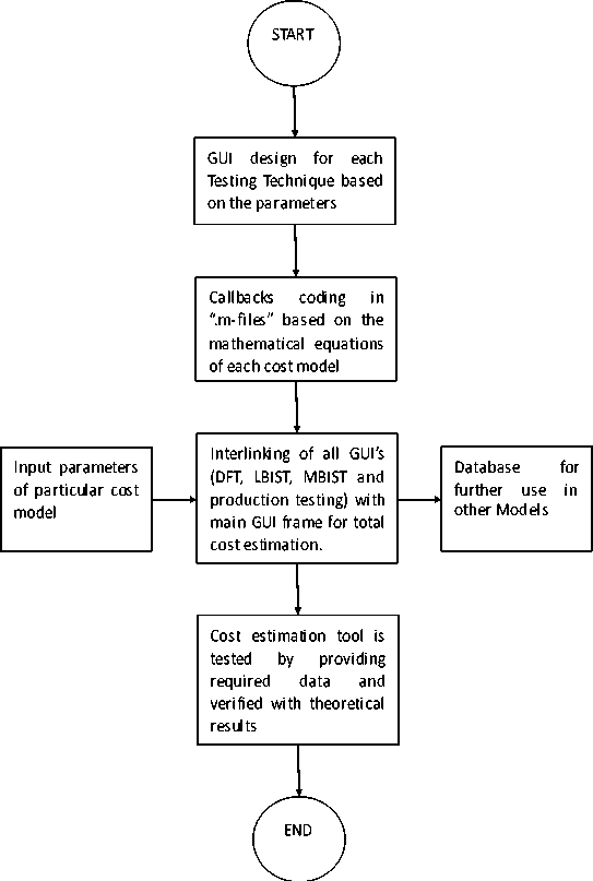
Figure 3: Flow the SOC testing cost
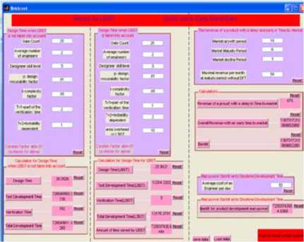
Figure 4. GUI for the cost model of the LBIST for analog and digital sections in the SOC.
Here designed GUI has been shown figure 4, includes the final cost result of the other GUIs which are designed differently for all the different aspects affecting the cost of SOC testing discussed above. It captures the results for the all subsections which includes the analog section, digital section with or without BIST and MBIST and other costs. That other cost results further include all the parameters which are discussed. All different subsections in the each GUI calculate the required cost parameters for which they are designed. The final cost results of one section are the input to the other, for further calculation inter linkage of all GUIs is done.
-
V. CASE STUDY FOR COST MODELING OF SOC MODULES TESTING
The developed Graphic User Interface in MATLAB environment based on the Cost Models from the various papers are tested by considering a case study for three devices; Device A, Device B Device C. table includes the results of MBIST. Here changes are forced in the area of the chip, average cost per engineer, development time in months, price of the memory test. These changes provide the change in cost of the product and overall benefits. These changes are observed satisfactorily on the designed frame work.
Table 1, includes the verification of LBIST cost models based design by considering the two cases; one for the model equations having no effect of LBIST parameters, and second is for LBSIT parameters into considerations. Then the effect of including LBIST is analyzed by providing the changes in number of gate counts, verification time for LBITS and without LBIST, and designer’s skill levels. Based on this changes in overall revenue can be analyzed examined. Table 2 give the effects and benefit of area overhead due to BIST circuits cost , In table 3 the consequence on overall area called area overhead is computed. Effects of increased area due to the self testing on chip modules like LBIST and MBIST are analyzed and its changes in the final cost and benefits are seen.
-
VI. CONCLUSION
The cost of testing integrated circuits and systems is growing rapidly as their complexity is increasing as per Moore’s law. Cost modeling plays a very important role in reducing test cost and time to market, it also gives estimate of overall testing. The economic modeling for VLSI testing with ATE and DFT is proposed. . The mathematical equations for ATE, DFT, BIST, MBIST and SOC are modeled using MATLAB GUI interface, which will give the exact estimation for the testing cost during VLSI testing process. The Graphical interface is provided for the test engineers which will be helpful to save time in cost calculations.
|
Cost due to Area Overhead |
||||
|
Area Overhead parameter |
Device A |
Device B |
Device C |
|
|
Area without LBIST |
15 |
15 |
15 |
|
|
Area overhead |
25 |
25 |
25 |
|
|
Defect density |
0.3 |
0.3 |
0.3 |
|
|
LBIST yield |
0.05 |
0.05 |
0.05 |
|
|
Production volume |
500 |
500 |
500 |
|
|
Cost per wafer |
0.05 |
0.05 |
0.05 |
|
|
Wafer radius |
5 |
10 |
0.3 |
|
|
cost per die |
2281.13 |
570.2825 |
633642721.29 4 |
|
|
Total Cost Benefit |
||||
|
Early market effect due to LBIST |
7213.9984 |
7213.9984 |
7213.998 4 |
|
|
Loaded man power benefits due to shorten development time |
2.2945 |
2.2945 |
2.2945 |
|
|
Total benefit using LBIST per die |
157648.6403 |
159359.4878 |
63204791 .5245 |
|
|
Benefit Due to Reduced Testing Cost |
||||
|
Annual description rate of tester |
5000 |
5000 |
5000 |
|
|
fsecond in one year |
31104000 |
31104000 |
31104000 |
|
|
Tester price to access chip without LBIST |
50 |
50 |
50 |
|
|
Tester time fo core without LBIST |
3600 |
3600 |
3600 |
|
|
Tester price for LBIST |
85 |
85 |
85 |
|
|
Tester for the pcre with LBIST |
600 |
600 |
1000 |
|
|
Production volume |
500 |
10000 |
10000 |
|
|
Cost savings due to BIST |
10368.44 |
207368.8272 |
152713.4 774 |
|
Table 1: Cost Parameters of LBIST and MBIST Testing
Table 2: Benefits of Area Overhead on Total Cost
|
Cost due to Extra Development Effort |
||||
|
Parameters for MBIST |
Device A |
Device B |
Device C |
|
|
Average Number of extra Engineers |
50 |
50 |
50 |
|
|
Average cost of extra Engineers |
20 |
200 |
250 |
|
|
Development time |
5 |
5 |
6 |
|
|
Cost |
$5000 |
$50000 |
$75000 |
|
|
Area |
2cm2 |
5cm2 |
7.5cm2 |
|
|
Memory capacity |
2 |
1000 |
10000 |
|
|
Area overhead for MBIST |
2.125 |
5.0459 |
7.5689 |
|
|
Silicon Cost due to Area -Overhead |
||||
|
Production volume |
500 wafers |
500 wafer |
500 wafers |
|
|
Cost / wafer |
0.00005 |
0.0005 |
0.00005 |
|
|
Radius of wafer |
0.005 |
0.05 |
0.005 |
|
|
Yield of MBIST |
0.01 |
0.01 |
0.01 |
|
|
Area |
20 |
20 |
20 |
|
|
Defect density |
0.5 |
0.5 |
0.5 |
|
|
Cost |
67994.441 |
17138.99 |
67994.4 4 |
|
|
Benefit due to Reduced Testing Cost |
||||
|
Production cost |
$5000 |
$5000 |
$5000 |
|
|
Annual description |
50 |
50 |
50 |
|
|
No. Of seconds in one year |
31104000 |
31104000 |
31104000 |
|
|
Price of a memory tester |
50 |
50 |
500 |
|
|
Tester time for the core without LBIST |
25 |
25 |
25 |
|
|
Time memory tester are used for chip with MBIST |
2000 |
2000 |
2000 |
|
|
Price of logic tester to access MBIST |
20 |
30 |
30 |
|
|
The time logic tester are used for chip with MBIST |
20 |
20 |
20 |
|
|
Benefit |
$4.0188 |
$2.6792 |
$62.9608 |
|
|
Parameters for overall cost test equations |
device A |
Device B |
device C |
|
Cost oftest development labour per unit time |
5 |
5 |
5 |
|
Cost of test development equipment per unit time |
10 |
10 |
10 |
|
Cost of design for test features |
15 |
15 |
15 |
|
Cost for floor space and factory infrastructure |
25 |
25 |
25 |
|
Cost of test equipment |
50 |
50 |
50 |
|
Cost for test labour |
15 |
15 |
15 |
|
Cost of reparing features |
30 |
30 |
30 |
|
Other cost of test |
12 |
12 |
12 |
|
Cost of sustsining issues |
8 |
8 |
8 |
|
Cost of capacity |
9 |
9 |
9 |
|
Capacity of buffer equipment |
5 |
5 |
5 |
|
Capacity of buffer available |
15 |
15 |
15 |
|
Volume required |
500 |
5000 |
5000 |
|
Time required |
70 |
70 |
70 |
|
Volume achievable |
450 |
4500 |
4500 |
|
Cost of over time |
15 |
15 |
15 |
|
Fault coverage |
10 |
25 |
50 |
|
Defect density |
0.1 |
0.1 |
0.1 |
|
Area of chip |
25 |
25 |
25 |
|
Risk factor |
2 |
2 |
2 |
|
Radius of wafer |
3 |
3 |
3 |
|
Manufacturing cost of an IC |
80 |
80 |
80 |
|
Cost of chip without fault tolerance factor |
75 |
75 |
75 |
|
Cost of the factory after 'n' times of period |
480 |
480 |
480 |
|
Number of time periods |
6 |
8 |
15 |
|
Overall cost of testing |
36731.6886 |
7222193.65 |
3254289134 3. |
|
Other cost total |
7.5 |
1.875 |
0.014648 |
References Cost Modeling for SOC Modules Testing
- International Technology Roadmap for Semiconductors (ITRS),” 2009. [Online]. Available: http://public.itrs.net
- Ricardo Reis, Marcelo Lubaszewski, Jochen A.G. Jess Design of Systems on a Chip: Design and Test, Published by Springer, P.O. Box 17, 3300 AA Dordrecht, the Netherlands.
- Soo Ho Chang and Soo Dong Kim Reuse-based Methodology in Developing System-on-Chip (SOC) Proceedings of the Fourth International Conference on Software Engineering Research, Management and Applications (SERA’06)
- Dear, I.D., Dislis, C., Ambler, A.P., Dick, J. 1991. Economic effects in design and test, Design & Test of Computers, IEEE, vol.8 (4,):64-77.
- Andrew C. Evans, 1999. Applications of Semiconductor Test Economics, and Multisite Testing to Lower Cost of Test, International Test Conference 1999 (ITC'99).
- Butler, K. M. 1999. Estimating the Economic Benefits of DFT. 16th IEEE Design. Test symposium 71-79.
- M. Abadir, A. Parikh, L. Bal, P. Sandborn, and C. Murphy, 1994. High Level Test Economics Advisor (Hi-TEA), Journal of Electronic Testing Theory and Practice, vol. 5, pp. 195–206.
- Karthik Sundararaman, Shambhu Upadhyaya, Martin Margala,” Cost Model Analysis of DFT Based Fault Tolerant SOC Designs,” 2004 IEEE.
- Li-Rong Zheng,” Cost and Performance Tradeoff Analysis in Radio and Mixed-Signal System-on-Package Design ,” IEEE Transactions on Advanced Packaging, Vol. 27, No. 2, May 2004.
- Songjun Lee and Anthony P. Ambler,” Cost Effective Test Planning For System-On-Chip Manufacture,” 2006 IEEE.
- Erik H. Volkerink, Ajay Khoche, Jochen Rivoir, Klaus D. Hilliges, 2002. Test Economics for Multi-site Test with Modern Cost Reduction Techniques, 20th IEEE VLSI Test Symposium, 411 – 416.
- Sudarshan Bahukudumbim, Sule Ozev, Krishnendu Chakrabarty, and Vikram Iyengar,” AWafer-Level Defect Screening Technique to Reduce Test and Packaging Costs for “Big-D/Small-A” Mixed-Signal SOCs,” 2007 IEEE.
- Frank Vahid and Tony Givargis Embedded System Design: A Unified Hardware/Software Introduction John Wiley & Sons; 2002.
- juin-Ming Lu; Cheng-Wen Wu, "Cost and benefit models for logic and memory BIST," Design, Automation and Test in Europe Conference and Exhibition 2000. Proceedings, vol., no., pp.710, 714, 2000.
- Nag, P.K.; Gattiker, A.; Sichao Wei; Blanton, R.D.; Maly, W., "Modeling the economics of testing: a DFT perspective," Design & Test of Computers, IEEE , vol.19, no.1, pp.29,41, Jan/Feb 2002.
- Kafrouni, M.; Thibeault, C.; Savaria, Y., "A cost model for VLSI/MCM systems," Defect and Fault Tolerance in VLSI Systems, 1997. Proceedings., 1997 IEEE International Symposium on , vol., no., pp.148,156, 20-22 Oct 1997.
- Sundararaman, K.; Upadhyaya, S.; Margala, M., "Cost model analysis of DFT based fault tolerant SOC designs," Quality Electronic Design, 2004. Proceedings. 5th International Symposium on, vol., no., pp.465, 469, 2004.
- Kim, V., Chen, T., and Tegethoff, M., ASIC Manufac turing Test Cost Prediction at Early Design Stage. IEEE international Test conference (1997) 356-6.
