Design and analysis of tunnel FET for low power high performance applications

Author: Umesh Dutta, M.K.Soni, Manisha Pattanaik
Journal: International Journal of Modern Education and Computer Science @ijmecs
Article in issue: 1 vol.10, 2018.
Free access
Tunnel FET is a promising device to replace MOSFET in low power high performance applications. This paper highlights and compares the best TFET designs proposed in the literature namely: Double gate Si-based TFET, InAs TFET device and III-V semiconductor (GaAs1-xSbx-InAs) based TFET device. Simulations are performed using TCAD tool and simulation results suggest that conventional DGTFET device has less on current and degraded subthreshold slope as compared to InAs and III-V semiconductor based TFET device. InAs based TFET device provides steep subthreshold slope of 61 mV/dec and off current of the order of nano-amperes at sub 1V operation thereby making it an ideal choice for low power high performance applications. The variation in the performance of the III-V HTFET device with the variation in the mole fraction is also studied in detail. Carefully choosing the mole fraction value in III-V semiconductor based HTFET device can lead to better device performance.
TFET, Parameter variation, Subthreshold swing, Leakage power, Reliability, Band to Band tunneling, High-K dielectric material, ITRS
Short address: https://sciup.org/15016731
IDR: 15016731 | DOI: 10.5815/ijmecs.2018.01.07
Text of the scientific article Design and analysis of tunnel FET for low power high performance applications
Published Online January 2018 in MECS DOI: 10.5815/ijmecs.2018.01.07
Tunnel FET device is one of the promising novel devices which is giving a threat to the conventional MOSFET device to be used for low power applications. TFET device operation is based upon band to band tunneling (BTBT) mechanism and it possesses very low leakage current and steep subthreshold slope. Subthreshold swing in case of MOSFET is ln(10) (KT/q) and at room temperature (300K), SS value is around 60
mV/dec. This fundamental challenge of reducing the SS value below 60mV/decade at room temperature can be easily overcome using a TFET device. TFET device also possess better Ion/Ioff ratio as compared to MOSFET and it is because of its low off current that TFET device is gaining confidence to be used in designing SRAMs for ultra low power applications. It is a well known fact that cache memory occupies almost 50% of the on chip area of the processor and reducing leakage in cache memory is a serious concern that needs to be addressed. A tunnel FET device possessing low off state current seems to be an immediate remedy for reducing leakage in cache memory.
A detailed description of zener tunneling and avalanche breakdown mechanism in As implanted n-p junctions had been described in detail in [1]. The main issue with a single gate TFET device is very low value of on current and poor subthreshold swing. A novel design for the double gate TFET (DGTFET) was proposed for the first time using high K dielectric material [2]. This novel device achieved SS of 57 mV/dec and an exceptionally high Ion/Ioff ratio. A novel structure of TFET device exhibiting higher on current than a conventional p-i-n TFET device was proposed in [3]. This structure was named as pocket doped TFET and has a pocket on the source side to improve the on current. Ambipolarity reduction was achieved using low doped drain extension. Modification in the TFET structure was required to be done so as to address the issue of poor on current and to achieve SS value of less than 60mV/dec. Different structures were proposed in the literature to overcome these limitations. To improve the tunneling current, low bandgap materials (eg. SiGe, Ge, InGaAs, InAs) have been widely explored for TFET prototype device design [4]. Electron Hole bilayer Tunnel FET (EHBTFET) structure had been proposed in [5] and this structure exploits the asymmetric bias configuration of a DGTFET device thereby creating the two carrier layers instead of one inside the thin silicon film. The bias applied at the bottom gate is fixed and the top gate bias is used to change the electron layer concentration thereby controlling the drain current. A novel device structure called Sandwitch Tunnel Barrier FET (STBFET) had been proposed in [6]. This novel structure overcomes the issue of large voltage overshoot that occurs in conventional TFET device. Schottky Tunneling Source SOI MOSFET (STS-FET) proposed in [7] has gate controlled schottky barrier tunneling at the source and possesses high immunity to short channel effects. Analysis of the leakage current of the pocket doped TFET device shows very less change with change in temperature [8]. This signifies that pocket doped TFET device has better temperature immunity as compared to MOSFET and conventional TFET device. Vertical InGaAs/InP heterojunction TFET had been proposed in [9] for the first time. Gate overlapped source and pocket doping approach were used in [10] to improve the performance of InGaAs/InP HTFET device. The concept of leakage reduction in vertical TFET structure was proposed in [11]. This new InAs based vertical TFET device structure achieves better Ion close to ITRS requirement and SS value of less than 60 mV/dec. The discussions made till now signifies that TFETs hold promising future in the IC world and are being explored by research fraternity over the years [12,29].
The rest of the paper is organized as follows: Section II describes the TFET device structure and its operation in detail. Concept of Subthreshold swing and challenges related to TFET device are discussed in section III. Section III also highlights the models used for performing simulations on Visual TCAD tool. Related work that is reported in the literature is presented in section IV. Simulation results of different TFET devices simulated in TCAD tool are highlighted in Section V. The effect of mole fraction parameter (x) on the performance of III-V HTFET device is discussed in Section VI and finally in Section VII conclusions are drawn.
-
II. Tfet Device Structure and Its Operation
The basic structure of nTFET consists of a p-i-n diode with the gate region covering the entire intrinsic region. Fig.1 shows the structure of nTFET in double gate configuration with p+ source region and n+ drain region. The structure can be regarded as a gated p-i-n diode in which tunneling of electrons takes place between p+ source and intrinsic region.
In the off state the energy barrier height is high enough so that the electrons cannot tunnel through the thick depletion region which exists across p+ source and intrinsic region and hence the off current is very low. When positive voltage is applied to the n+ region and gate is also made positive with reference to the p+ source region then there occurs band bending and reduction in the energy barrier height which increases the probability of inter-band tunneling of electrons from valance band of p+ source region to the conduction band of the intrinsic region. The TFETs exhibit gate bias dependent NDR characteristics at room temperature under forward bias confirming band to band tunneling [13].
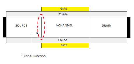
Fig.1. Basic DGTFET device structure.
Energy band diagram at different V GS values shows band gap narrowing effect and band bending which increases the tunneling probability across the tunnel junction. Fig.2. shows the band diagram plot of n-type DGTFET device at V GS =0V and V DS =1V and Fig.3 shows the band diagram plot at VGS=1V and VDS=1V.
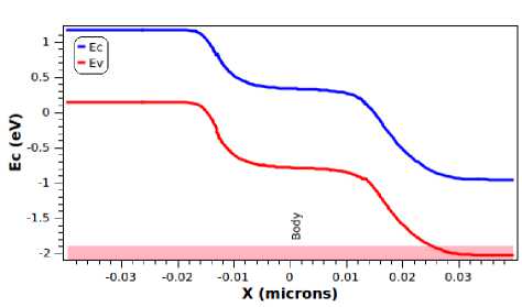
Fig.2. Band diagram of DGTFET device at V GS =0V and V DS =1V.
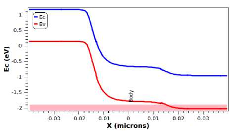
Fig.3. Band diagram of DGTFET device at V GS =1V and V DS =1V
Comparative band diagram is shown in Fig.4. It clearly shows that band gap reduction takes place with change in V GS value. A point to note is that both band bending and band gap narrowing takes place with increase in V GS value.
The challenge of enhancement of the on current in tunnel FET can be addressed by using a lower energy band gap material rather than silicon thereby enhancing the tunneling probability across the tunnel junction. Materials like Ge, InAs, III-V compound semiconductors exhibits lower Eg value and can be used for the fabrication of TFET device. On current of the similar order can be achieved as it can be achieved using a MOSFET device. Using germanium in the source region can lead to small tunnel band gap and leads to improvement in the energy efficiency of the TFET device [14].
Boucart et al. [12] had proposed an analytical expression that can be used for the calculation of average sub-threshold swing of TFET device.
Average Subthreshold Swing =
Vth - Voff
1 ( Ith log
I M
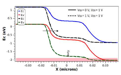
Fig.4. Comparative Band diagram of DGTFET device.
where Voff is the gate source voltage at which drain current is minimum ( Ioff ), Vth is the threshold voltage at the threshold point (point at which Ids is 10-7 A/um). A practical expression for calculating the effective sub threshold swing of TFET device was proposed in [16]. According to this new practical definition:
Vth = Vdd and Ith = Ids(Vgs=Vdd/2) 2
Voff = 0 and Ioff = Ids (Vgs=0)
Hence Subthreshold Swing expression can be rewritten as-
SS = Vdd! [2 log( Ith / loff )].
-
III. Subthreshold Swing and Reliability Issues
Subthreshold swing in TFETs is defined in the same way as it is done in MOSFETs which means that it is the gate voltage which must be applied with respect to source so as to increase the drain current by one decade. A formula for calculating the subthreshold swing of TFET is proposed in [15]. This formula shows that SS of TFET is not limited to 60mV/decade. Mathematically Subthreshold Swing (SS) can be expressed as-
Subthreshold Swing =
dVg d (log Id )
mV / dec .
The subthreshold swing of MOSFET is limited to 60mV/dec at T=300K (room temperature) and this limitation can be overcome in TFETs which rely on interband tunneling via barrier width modulation rather than the formation of weak inversion channel between source and drain. Point sub threshold swing is the smallest value of the subthreshold swing on the ID-VG curve and on the other hand average subthreshold swing is calculated from the point where the device starts to turn on up to the threshold point (defined using constant current method [12]). The subthreshold swing in TFET is strongly dependent on the gate bias and for analyzing the switching performance it is better to consider average subthreshold swing rather than the point subthreshold swing. Literature indicates that the inherent issue of lower tunneling current that exists in silicon because of relatively higher energy band gap and lower effective tunneling mass has encouraged the designers to deploy lower band gap materials for the fabrication of TFET. Materials like Ge, InAs, GNRs, Heterojunction materials (SiGe/Si, AlGaSb/InAs, AlGaAsSb/InGaAs) etc. leads to a significant increase in the on current of TFET.
SS value decreases as Vgs value decreases. Vgs directly controls the tunnel junction bias (band overlap). Gate is placed to align the field with the internal field at the tunnel junction. Gate field adds to the internal field and increases the tunneling probability.
Cogenda Visual TCAD is used for performing device simulations. Kane’s Local BTBT model is used along with SRH model for device simulation. For mobility Lombardi model is used in this work. A method to calculate the parameters A and B of Kane’s direct and indirect tunneling models at different tunneling directions for Si, Ge and Si 1-x Ge x was discussed in [17]. The calculation of band-to-band generation rate in uniform electric field reveals that direct tunneling always dominates over indirect tunneling in Ge [17].
Kane’s Band to Band Tunneling Model:
Kane’s tunneling model is used in the simulator to calculate the carrier generation by band to band tunneling phenomenon. The carrier generation rate is calculated using the following expression derived from [17].
2 ( F 3/2
Challenges in TFET:
Unlike CMOS, TFETs exhibit unidirectional conduction due to their asymmetric source-drain architecture [18,31]. TFET operates at low supply voltage range (Vdd< 0.5V) to outperform CMOS, reliability issues can have profound impact on the circuit design from practical application perspective [19]. Subthreshold swing of TFET is found to be more robust against PBTI as compared with MOSFETs [20]. Charges present in the Si-Oxide interface and Oxide-Oxide interface affects the performance of the TFET device. Tunnel FETs also show relatively less variation to fixed interface charges and can replace MOSFETs in circuits to combat against NBTI and PBTI effects [21]. Investigation of p-n-i-n TFET device carried out in [22] reveals that TFET structure has improved reliability as compared to conventional TFET structure. Reduced interface trap generation and gate leakage is seen in p-n-i-n TFET along with less variation in the threshold voltage with change in the oxide thickness and Si film thickness. The gate dielectric plays an important role in enhancing the performance of a p-n-p-n TFET device. In p-n-p-n TFET device use of high gate dielectric constant is preferable for enhancing the gate control over the channel, while a low fringe dielectric constant is useful to increase band to band tunneling probability [23]. Use of spacer in TFET device leads to suppression in the ambipolar conduction [24]. Overlapping the gate on the drain can also suppress the ambipolar conduction, which is an inherent property of a TFET device [25]. Doping Less Tunnel FET device is expected to be free from random dopant fluctuation [26] and this configuration also possesses similar performance as that of the corresponding doped TFET device. Use of TFET device in low power high performance application circuits like SRAM can lead to several advantages like improvement in the noise margins, power reduction and reliability. Different SRAM cell topologies are proposed in [12,19,27] have shown tremendous performance under ultra low supply voltage and thereby showing the possibility of designing complete TFET based SRAM. DGTFET-based dynamic memory at sub-100-nm regime has been discussed in detail in [30] with main emphasis on device optimization by tuning the misalignment, lateral spacing between the gates ( L gap ) and an underlap ( L un ) between the back gate and drain region.
-
IV. Related Work
References Design and analysis of tunnel FET for low power high performance applications
- B. F. Richard, and W. W. Hayden, “ Zener and Avalanche Breakdown in As- Implanted Low-Voltage Si n-p Junctions,” IEEE Trans. on Electron Devices, vol. 23, no.5, pp.512-518, May 1976.
- K. Boucart, and A. M. Ionescu, “Double-Gate Tunnel FET With High-k Gate Dielectric,” IEEE Trans. on Electron Devices, vol. 54, no. 7,pp. 1725-1733, Jul. 2007.
- R. Jhaveri, V. Nagavarapu, and J.C.S. Woo, “ Effect of Pocket Doping and Annealing Schemes on the Source- Pocket Tunnel Field- Effect Transistor,” IEEE Trans. on Electron Devices, vol. 58, no. 1, pp. 80-86, Jan. 2011.
- H. Liu, S. Dutta, III-V Tunnel FET model manual, 2015, [online] Available: https://nanohub.org/publications/12/2.
- L.Lattanzio,D. L. Michielis, and A.M. Ionescu, “Electron-hole bilayer tunnel FET for steep subthreshold swing and improved ON current,” IEEE Solid-State Dev. Research Conference (ESSDERC), pp. 259-262, 2011, Sept. 2011.
- R. Asra, M. Shrivastava, K. VRM Murali, R. K. Pandey, H. Gossner, and V. R. Rao, “A Tunnel FET for VDD Scaling Below 0.6 V With a CMOS – Comparable Performance,” IEEE Trans. on Electron Devices, vol. 58, no. 7, pp. 1855-1863, Jul. 2011.
- R. Jhaveri, V. Nagavarapu, and J. C. S. Woo, “ Asymmetric Schottky Tunneling Source SOI MOSFET Design for Mixed- Mode Applications,” IEEE Trans. on Electron Devices, vol.56, no.1, pp.93-99, Jan.2009.
- A. Mishra, K.K. Jha, M. Pattanaik, “ Parameter variation aware hybrid TFET-CMOS based power gating technique with a temperature variation tolerant sleep mode,” Microelectronics Journal, vol. 45, no. 11, pp. 1515-1521, Nov. 2014.
- G. Zhou, L. Yeqing, L. Rui, Z. Qin, S. H. Wan, L. Qingmin, V. Tim, et al. “Vertical InGaAs/InP tunnel FETs with tunneling normal to the gate,” IEEE Electron Device Letters, vol. 32, no. 11, pp. 1516-1518, Nov. 2011.
- S. Sant, and A. Schenk, “Methods to enhance the Performance of InGaAs/InP Heterojunction Tunnel FET’s,” IEEE Trans. on Electron Devices, vol. 63, no.5, pp. 2169-2175, May 2016.
- S. Agarwal, G. Klimeck, and M. Luisier, “Leakage- Reduction Design Concepts for Low-Power Vertical Tunneling Field- Effect Transistors,” IEEE Electron Device Letters, vol. 31, no. 6, pp. 621-623, Jun. 2010.
- M. K. Z. Ansari, S. Ahish, D. Sharma, M. H. Vasantha, and YB Nithin Kumar, “Performance analysis of a novel hetero-junction tunnel FET based SRAM at 0.3 V supply voltage,” IEEE Technology Symposium (TechSym), pp. 224-228, Sep. 2016.
- S. Mookerjea, D. Mohata, R. Krishnan, J. Singh, A. Vallett,A. Ali, T. Mayer, V. Narayanan, D. Schlom,A. Liu, and S. Datta, “ Experimental demonstration of 100nm channel length In0.53Ga0.47As-based vertical inter-band tunnel field effect transistors (TFETs) for ultra low-power logic and SRAM applications,” IEEE Electron Devices Meeting (IEDM), pp.1-3, Dec. 2009.
- Kim, S.H., Kam, H., Hu, C. and Liu, T.J.K. “Germanium-source tunnel field effect transistors with record high I ON/I OFF,” IEEE VLSI Technology, 2009 Symposium IEEE, pp. 178-179, Jun. 2009.
- Z, Qin, W. Zhao, and A. Seabaugh, “Low-subthreshold-swing tunnel transistors,” IEEE Electron Device Letters., vol. 2, no. 4, pp. 297-300, Apr. 2006.
- A. C. Seabaugh, and Q. Zhang, “Low-Voltage Tunnel Transistors for Beyond CMOS Logic,” Proceedings of the IEEE, vol. 98, no. 12, pp. 2095-2110, Dec. 2010.
- K-H. Kao, S. V. Anne, G. V. William, S. Bart, G. Guido, and D. M. Kristin “Direct and indirect band-to-band tunneling in germanium-based TFETs,” IEEE Trans. on Electron Devices, vol. 59, no. 2, pp. 292-301, Feb. 2012.
- V. Saripalli, S. Datta, V. Narayanan, and J. P. Kulkarni, “Variation-tolerant ultra low-power heterojunction tunnel FET SRAM design,” IEEE/ACM International Symposium on Nanoscale Architectures, pp. 45-52, Jun. 2011.
- S. Dutta, H. Liu, and V. Naraynan,“Tunnel FET Technology: A reliability perspective,” Microelectronics Reliability, vol. 54, no. 5, pp. 861-874, May 2014.
- J. Franco, A. Alian, A. Vandooren, A. S. Verhulst, D. Linten, N. Collaert, and A. Thean, “Intrinsic robustness of TFET subthreshold swing to interface and oxide traps: A comparative PBTI study of InGaAs TFETs and MOSFETs,” IEEE Electron Device Letters, vol. 37, no. 8,pp. 1055-1058, Aug. 2016.
- A. Mishra, R. Narang, M. Saxena, and M. Gupta, “Impact of Interfacial Fixed Charges on the Electrical Characteristics of Pocket-Doped Double-Gate Tunnel FET,” IEEE Trans. on Device and Materials Reliability,vol. 16, no. 2, pp. 117-122, Jun. 2016.
- W. Cao, C. J. Yao, G. F. Jiao, D. Huang, H. Y. Yu and M. F. Li, “Improvement in Reliability of Tunneling Field-Effect Transistor With p-n-i-n Structure,” IEEE Trans. on Electron Devices, vol. 58, no. 7, pp. 2122-2126, Jul. 2011.
- C. Ning, L. Renrong, W. Jing, Z. Wei, and X Jun, “A PNPN tunnel field-effect transistor with high-k gate and low-k fringe dielectrics,” Journal of Semiconductors, vol. 33, no. 8, pp.084004-1-084004-6, Aug.2012.
- C. Anghel, Hraziia, A. Gupta, A. Amara and A. Vladimirescu,“30-nm Tunnel FET With Improved Performance and Reduced Ambipolar Current,” IEEE Trans. on Electron Devices, vol. 58, no. 6, pp. 1649-1654, Jun. 2011.
- D. B. Abdi, and M. Jagadesh Kumar, “Controlling Ambipolar Current in Tunneling FETs Using Overlapping Gate-on-Drain,” IEEE Journal of the Electron Devices Society, vol. 2, no. 6, pp. 187-190, Nov. 2014.
- M. J. Kumar, and S. Janardhanan, “ Doping-less Tunnel Field Effect Transistor: Design and Investigation,” IEEE Trans. on Electron Devices., vol. 60, no. 10, pp. 3285-3290, Oct. 2013.
- J. Singh, K. Ramakrishnan, S. Mookerjea, S. Datta, N. Vijaykrishnan, and D. Pradhan, “A novel si-tunnel FET based SRAM design for ultra low-power 0.3 VV DD applications,” IEEE Proceedings Asia and South Pacific Design Automation Conference, pp. 181-186, Jan. 2010.
- T.Waho, S.Ogawa and S.Maruyama, “GaAs1-xSbx (0.3< x< 0.9) grown by molecular beam epitaxy,” Japanese Journal of Applied Physics, vol.16, no.10, pp.1875-1876, Oct. 1977.
- Pandey, Rahul, Saurabh Mookerjea, and Suman Datta, “Opportunities and Challenges of Tunnel FETs,” IEEE Transactions on Circuits and Systems I: Regular Papers, vol.63, no.12, pp.2128-2138, Dec. 2016.
- Navlakha N, Lin JT, Kranti A, “Retention and Scalability Perspective of Sub-100-nm Double Gate Tunnel FET DRAM,” IEEE Transactions on Electron Devices, vol.64, no.4, pp.1561-1567, April 2017.
- Safa S, Noor SL, Khan ZR, “Physics-Based Generalized Threshold Voltage Model of Multiple Material Gate Tunneling FET Structure,” IEEE Transactions on Electron Devices, vol. 64, no.4, pp. 1449-1454, April 2017.
