Design and Development MIPS Processor Based on a High Performance and Low Power Architecture on FPGA

Author: Tina Daghooghi
Journal: International Journal of Modern Education and Computer Science (IJMECS) @ijmecs
Article in issue: 5 vol.5, 2013.
Free access
This paper presents the design and development of a high performance and low power MIPS microprocessor and implementation on FPGA. In this method we for achieving high performance and low power in the operation of the proposed microprocessor use different methods including, unfolding transformation (parallel processing), C-slow retiming technique, and double edge registers are used to get even reduce power consumption. Also others blocks designed based on high speed digital circuits. Because of feedback loop in the proposed architecture C-slow retiming can enhance designs that contain feedback loops. The C-slow retiming is well-known for optimization and high performance technique, it automatically rebalances the registers in the proposed design. The proposed high performance microprocessor is modeled and verified using FPGA and simulation results. The proposed methods in microprocessor have been successfully synthesized and implemented in Quartus II 9.1 and Stratix II FPGA, to target device EP2S15F484C3, and power is analyzed with Xpower analyzer. Results demonstrate that the proposed method has high performance.
High Performance, Low Power, FPGA, double edge register, Combinational Logic
Short address: https://sciup.org/15014549
IDR: 15014549
Text of the scientific article Design and Development MIPS Processor Based on a High Performance and Low Power Architecture on FPGA
Published Online June 2013 in MECS DOI: 10.5815/ijmecs.2013.05.06
Microcontrollers and microprocessors are used in everyday systems. Basically, any electronic systems that require computation or instruction execution require a microcontroller or microprocessor. Therefore, at the core of electronic systems with computational capability is a microprocessor. Microprocessors have grown from 8 bits to 16 bits, 32 bits, and currently to 64 bits. Microprocessor architecture has also grown from complex instruction set computing (CISC) based on reduced instruction set computing (RISC) based on a combination of RISC-CISC based and currently very long instruction word (VLIW) based [1]. Some microprocessors are optimized for high-performance servers, whereas others are optimized for long battery life in laptop computers. A computer architecture is defined by its instruction set and architectural state. The architectural state of the MIPS processor consists of the program counter and the 32 registers. Any MIPS micro architecture must contain all of this state. Based on the current architectural state, the processor executes a particular instruction with a particular set of data to produce a new architectural state. Some microarchitectures contain additional nonarchitectural state to either simplify the logic or improve performance [2]. The IBM System z10™ microprocessor is currently the fastest running 64-bit CISC (complex instruction set computer) microprocessor. This microprocessor operates at 4.4 GHz and provides up to two times performance improvement compared with its predecessor, the System z9® microprocessor. In addition to its ultrahigh-frequency pipeline, the z10™ microprocessor offers such performance enhancements as a sophisticated branch-prediction structure, a large second-level private cache, a data-prefetch engine, and a hardwired decimal floating-point arithmetic unit. The z10 microprocessor also implements new architectural features that allow better software optimization across compiled applications. These features include new instructions that help shorten the code path lengths and new facilities for software-directed cache management and the use of 1-MB virtual pages [3].
In recent years, a number of researches have been proposed for Implementation of microprocessor by using the FPGA by some companies [4-11]. In continuing we present some researches, The Aviation Microelectronic Center of NPU (Northwestern Polytechnical University) has recently completed the development of a 32-bit super-scalar RISC microprocessor, called "Longtium" R2. In [4], the architecture of "Longtium" R2 is presented. As explained in [5], the PowerPC 603e microprocessor is a high performance, low cost, low power microprocessor designed for use in portable computers. The 603e is an enhanced version of the PowerPC 603 microprocessor and extends the performance range of the PowerPC microprocessor family of portable products. The enhancements include increasing the frequency to 100 MHZ doubling the on-chip instruction and data caches to 16K bytes each, increasing the cache associativity to 4-way set-associative, adding an extra integer unit, and increasing the throughput of stores and misaligned accesses. Three new bus modes are added to allow for more flexibility in system design. The estimated performance of the 603e at 100 MHz is 120 SPECint92 and 105 SPECfp92. In [6], a new microprocessor design framework, called DOTTA
(dynamic operation transport triggered array) is introduced. An FPGA (field programmable gate array) implementation of DOTTA is presented. The aim of this new processor framework is to eliminate bottlenecks introduced by traditional microprocessor architectures. The framework defines a task-specific microprocessor that is application customisable on the target system it is operating on; this has been achieved by using Xilinxtrade FPGA fabric. In [7], a 8-bit CISC microprocessor core development which is intended as an open core for teaching applications in the digital systems laboratory. The core is fully open and therefore, the user can have access to all internal signals as well as the opportunity to make changes to the structure itself which is very useful when lecturing microprocessor design. The main advantages of the present core, compared with commercially available equivalent cores, are not being vendor sensitive allowing its implementation in almost any FPGA family and being an open core, that can be fully monitored and modified to fit specific design constraints. Several tests were performed to the microprocessor core, including an embedded microcontroller with RAM, ROM and I/O capabilities. The present development includes a metaassembler and linker to embed user programs in a ROM, which is automatically generated as a VHDL description. In [8], a new methodology based on practical sessions with real devices and chips is proposed. Simple designs of microprocessors are exposed to the students at the beginning, raising the complexity gradually toward a final design with a multiprocessor integrated in a single FPGA chip. In [9], the implementation and delivery of a microprocessor based on laboratory design is presented design laboratory, in an attempt to achieve tighter integration with theory and improve student's performance. The design process follows a hierarchical structure, requiring students to first build basic devices such as logic gates, multiplexers, one-bit memory cells etc. These basic devices are then used to build an ALU, registers, (registers are used to build larger memories), a data path and a control unit. Designs are completed without any high level programming ensuring that students cannot rely on the compiler to transform specifications into implementations. In [10], several case studies that examine the effects of various embedded processor memory strategies and peripheral sets. Comparing the benchmark system to a real-world system, the study examines techniques for optimizing the performance and cost of an FPGA embedded processor system. The development of a microprocessor based on automatic gate is presented by [11]. The inconvenience encountered in gate operations has called for an immense search for solutions. The microprocessor based on automatic gate offers everything necessary to put an end to these inconveniences as it incorporates an intelligent device (microprocessor). The automatic gate developed their project is unique in that it is controlled by software, which can be modified any time the system demands a change. The main goal of this paper is to design a high performance microprocessor with a novel way on FPGA. We applied several methods to microarchitecture the performances and the effectiveness of the proposed methods of the throughput rate and hardware cost for the proposed structure are given. This paper is organized as follows. An overview of the MIPS processor will be given in section II. In section III description of the proposed methods is presented. A comparison of performance, power consumption, chip utilization that verifies the performance of the proposed work is focus of section IV. In section V conclusion of the paper is presented.
-
II. MIPS PROCESSOR
MIPS is a 32-bit architecture, so its a 32-bit data path. The control unit receives the current instruction from the data path and tells the datapath how to execute that instruction. Specifically, the control unit produces multiplexer select, register enable, and memory writes signals to control the operation of the data path. The program counter is an ordinary 32-bit register. Its output, PC, points to the current instruction. Its input, PC , indicates the address of the next instruction. The instruction memory has a single read port. It takes a 32-bit instruction address input, A, and reads the 32-bit data (i.e., instruction) from that address onto the read data output, RD. The 32-element x 32-bit register file has two read ports and one write port. The read ports take 5-bit address inputs, A1 and A2, each specifying one of 25=32 registers as source operands. They read the 32-bit register values onto read data outputs RD1 and RD2, respectively. The write port takes a 5-bit address input, A3; a 32-bit write data input, WD; a write enable input, WE3; and a clock. If the write enable is 1, the register file writes the data into the specified register on the rising edge of the clock. The data memory has a single read/write port. If the write enable, WE, is 1, it writes data WD into address A on the rising edge of the clock. If the write enable is 0, it reads address A onto RD. The instruction memory, register file, and data memory are all read combinationally. In other words, if the address changes, the new data appears at RD after some propagation delay; no clock is involved. They are written only on the rising edge of the clock. In this fashion, the state of the system is changed only at the clock edge. The address, data, and write enable must setup sometime before the clock edge and must remain stable until a hold time after the clock edge. Because the state elements change their state only on the rising edge of the clock, they are synchronous sequential circuits. The microprocessor is built on clocks state elements and combinational logic, so it too is a synchronous sequential circuit. Indeed, the processor can be viewed as a giant finite state machine, or as a collection of simpler interacting state machines [2]. To keep the microarchitectures easy to understand, we consider only a subset of the MIPS instruction set:
-
1- R-type arithmetic/logic instructions: add, sub, and, or, slt
-
2- Memory instructions: lw, sw
-
3- Branches: beq
-
A. MIPS Microarchitectures
In this part, based on [2], a MIPS microarchitecture executes instructions in a single cycle. The first step is to read this instruction from instruction memory. That the PC is simply connected to the address input of the instruction memory. The instruction memory reads out, or fetches, the 32-bit instruction, labeled Instr. The processor’s actions depend on the specific instruction that was fetched. For a lw instruction, the next step is to read the source register containing the base address. This register is specified in the rs field of the instruction, Instr 25 : 21 . These bits of the instruction are connected to the address input of one of the register file read ports, A1. The register file reads the register value onto RD1.
The lw instruction also requires an offset. The offset is stored in the immediate field of the instruction, Instr15:0. Because the 16-bit immediate might be either positive or negative, it must be sign-extended to 32 bits. The 32-bit sign-extended value is called SignImm. Sign extension simply copies the sign bit of a short input into all of the upper bits of the longer output. Specifically, SignImm15:0 = Instr15:0 and SignImm31:16 = Instr15. The processor must add the base address to the offset to find the address to read from memory. Introduces an ALU to perform this addition. The ALU receives two operands, SrcA and SrcB. SrcA comes from the register file, and SrcB comes from the sign-extended immediate. The ALU can perform many operations. The 3-bit ALUControl signal specifies the operation. The ALU generates a 32-bit ALUResult and a Zero flag, that indicates whether ALUResult == 0. For a lw instruction, the ALUControl signal should be set to 010 to add the base address and offset. ALUResult is sent to the data memory as the address for the load instruction, as shown in Fig.1. The data is read from the data memory onto the ReadData bus, then written back to the destination register in the register file at the end of the cycle, Port 3 of the register file is the write port. The destination register for the lw instruction is specified in the rt field, Instr20:16, which is connected to the port 3 address input, A3, of the register file. The ReadData bus is connected to the port 3 write data input, WD3, of the register file. A control signal called RegWrite is connected to the port 3 write enable input, WE3, and is asserted during a lw instruction so that the data value is written into the register file. While the instruction is being executed, the processor must compute the address of the next instruction, PC . Because instructions are 32 bits = 4 bytes, the next instruction is at PC + 4. Uses another adder to increment the PC by 4. The new address is written into the program counter on the next rising edge of the clock. This completes the data path for the lw instruction. Like the lw instruction, the sw instruction reads a base address from port 1 of the register and signextends an immediate. The ALU adds the base address for the immediate to find the memory address. The register is specified in the rt field, Instr20:16. These bits of the instruction are connected to the second register file read port, A2. The register value is read onto the RD2 port. It is connected to the write data port of the data memory. The write enable port of the data memory, WE, is controlled by MemWrite. For a sw instruction, MemWrite= 1, to write the data to memory; ALUControl = 010, to add the base address and offset; and RegWrite = 0, because nothing should be written to the register file. The R-type instructions read two registers from the register file, and write the result back to a third register file. They differ only in the specific ALU operation, using different ALUControl signals.
The register file reads two registers. The ALU performs an operation on these two registers. In Fig.1, the ALU always receives its SrcB operand from the sign-extended immediate (SignImm). A multiplexer choose SrcB from either the register file RD2 port or SignImm. The multiplexer is controlled by a new signal, ALUSrc. ALUSrc is 0 for R-type instructions to choose SrcB from the register file; it is 1 for lw and sw to choose SignImm. The register file always gets its write data from the data memory. However, R-type instructions write the ALUResult to the register file. Therefore, another multiplexer is needed to choose between ReadData and ALUResult. That calls its output Result. This multiplexer is controlled by another new signal, MemtoReg. MemtoReg is 0 for R-type instructions to choose a result from the ALUResult; it is 1 for lw to choose ReadData. The register to write was specified by the rt field of the instruction, Instr 20 : 16 . However, for R-type instructions, the register is specified by the rd field, Instr 15 : 11 . Thus, add a third multiplexer to choose WriteReg from the appropriate field of the instruction. The multiplexer is controlled by RegDst. RegDst is 1 for R-type instructions to choose WriteReg from the rd field, Instr 15:11 ; it is 0 for lw to choose the rt field, Instr 20:16 . Finally, beq compares two registers. If they are equal, it takes the branch by adding the branch offset to the program counter. That the offset is a positive or negative number, stored in the imm field of the instruction, Instr31:26. The offset indicates the number of instructions to branch past. Hence, the immediate must be sign-extended and multiplied by 4 to get the new program counter value: PC =PC+4+ SignImm x 4. The next PC value for a taken branch, PCBranch, is computed by shifting SignImm left by 2 bits, then adding it to PCPlus4. The left shift by 2 is an easy way to multiply by 4, because a shift by a constant amount involves just wires. The two registers are compared by computing SrcA-SrcB using the ALU. If ALUResult is 0, as indicated by the Zero flag from the ALU, the registers are equal. A multiplexer chooses PC from either PCPlus4 or PCBranch. PCBranch is selected if the instruction is a branch and the Zero flag is asserted. Hence, Branch is 1 for beq and 0 for other instructions. For beq, ALUControl =110, so the ALU performs a subtraction. ALUSrc = 0 to choose SrcB from the register file. RegWrite and MemWrite are 0, because a branch does not write to the register file or memory.
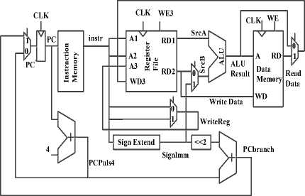
Figure 1: MIPS processor with single cycle datapath.
The pipelined datapath is formed by chopping the single cycle datapath into five stages separated by pipeline registers. Fig.2 shows the pipelined datapath formed by inserting four pipeline registers to separate the datapath into five stages. Signals are given a suffix (F, D, E, M, or W) to indicate the stage in which they reside. The register file is peculiar because it is read in the Decode stage and written in the Writeback stage. It is drawn in the Decode stage, but the write address and data come from the Writeback stage. This feedback will lead to pipeline hazards. The register file write logic should operate in the Writeback stage. The data value comes from ResultW, a Writeback stage signal. But the address comes from WriteRegE, an Execute stage signal. The WriteReg signal is pipelined along through the Memory and Writeback stages, so it remains in sync with the rest of the instruction. WriteRegW and ResultW are feedback together in the register file in the Writeback stage. The astute reader may notice that the PC logic is also problematic, because it might be updated with a Fetch or a Memory stage signal (PCPlus4F or PCBranchM).
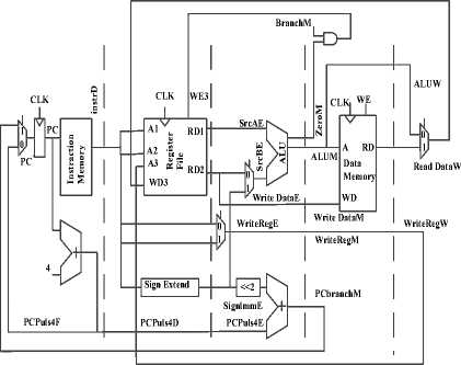
Figure.2: MIPS processor with pipelined datapath.
We simply analyze using Data Flow Graph (DFG), thus we should convert microarchitecture (MIPS processor) to DFG in this proposed DFG we consider only main blocks of microarchitecture including: Instruction Memory (IM), Register File (RF), ALU (A), Data Memory (DM). The proposed DFG of MIPS processor is shown in Fig.3 this DFG is included feedback loops.
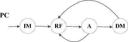
Figure.3: Proposed DFG of MIPS processor.
-
III. Proposed methods
This part of paper is considered in explaining proposed methods, now in continuing our description any method in the following sections. The goal of this work, is the design and development of one high performance microprocessor based on MIPS processor thus using several techniques. The design composed these different techniques, all parts are interconnected with each other to perform the designed method task to achieve high performance and high speed.
-
A. Unfolding Transformation
Unfolding is a transformation technique to change the program into another program such that one iteration of the new program describes more than one iteration in the original program. Also used to design bit parallel and word parallel architectures from bit serial and word serial architecture. Base on unfolding is same parallel processing. This technique can be used in Sample period reduction and parallel processing.
-
a. Algorithm for Unfolding
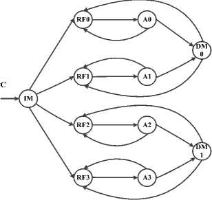
Word-level parallel processing, Bit level parallel processing is included: Bit-serial processing, Bit-parallel processing, and Digit-serial processing. In the proposed method we use unfolding technique and design proposed architecture base on 4 level parallel processing. Until increase speed of data process. Fig.4 shows the interconnection between different system blocks. As seen proposed design based on 4 level parallel processing (unfolded), DM0 and DM1 are Dual Port RAM (DPRAM).
RF2
A2
Figure.4: Proposed design based on 4 level parallel processing (unfolded).
-
b. Sample Period Reduction
For each node U in the original DFG, draw J node U 0 , U1, U 2 , U j-i . Also for each edge U ^ V with w delays in the original DFG, draw the J edges Ui ^ V (I + w) % J with L (i+w) /J (delays for I = 0, 1, J-1. The DFG in Fig 5 is unfolded using unfolding factor 4 to get the DFG in Fig. 5(b). Note that unfolding of an edge with w delays in the original DFG produces j-w edges with no delays and w edges with 1 delay in j-unfolded DFG when unfolding of an edge with w delays in the original DFG when w < j.
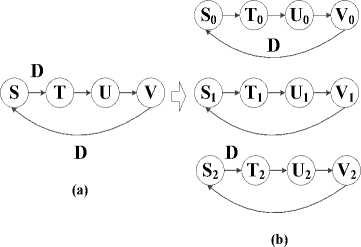
Figure.6: (a) The original DFG with iteration bound T=4/3 and minimum sample period of 2. (b) The 3-unfolded DFG with iteration bound T=4 and minimum sample period of 4/3.


(a)
W = 37
L ( i + W )/4 j = 9, i = 0,1,2 = 10, i = 3
U0 9D
U1 9D
U2
U3 10D
(b)
Figure.5: Unfolding of an edge with w delays in the original DFG.
Unfolding of an edge with w delays in the original DFG produces J-w edges with no delays and w edges with 1delay in J unfolded DFG for w < J. Unfolding preserves precedence constraints of a DSP program. Applications of Unfolding include: Sample Period Reduction, Parallel Processing.
-
c. Parallel processing
Iteration bound is not an integer. The original DFG cannot have sample period equal to the iteration bound because the iteration bound is not an integer. If a critical loop bound is of the form t l /w l where t l and w l are mutually co-prime, then w l -unfolding should be used. In the example tl=60 and wl=45, then tl/wl should be written as 4/3 and 3-unfolding should be used. A simple example of this is shown Fig 6(a), where the DFG has iteration bound T=4/3; however, even retiming cannot be used to achieve a critical path of less than 2. This DFG can be unfolded DFG has iteration bound T=4, and its critical path is 4. The unfolded DFG performans 3 iterations of the original problem in 4, so the sample period of the unfolded DFG is 4/3, which is the same as the iteration bound of the original DFG. To summarize, the original DFG in Fig5(a) cannot achieve a sample period equal to the iteration bound because the itration bound is not an integer, but the unfolded DFG in Fig 5(b) can have a sample period equal to the iteration bound of the original DFG. In general, if a critical loop bound is of the form t1/w1 where t1 and wl are mutually coprime, then wl-unfolding should be used.
-
B. C-Slow Retiming
Although pipelin ing is a huge benfiet FPGA design , and may be required on some FPGA fabrics it is often difficult for a designer to manage and balance pipeline stages and to insert the necessary delays to meet design requirements. Leiserson et al. Were thefirst t o propose returning, an automatic process to relocate pipeline stages to balance a design. Their algorithm, in O (n2lg (n)) time, can rebalance a design so that the critical path is optimally pipelined. In addition, two mfiocadtiions, repipelining and C-slow retiming, can add additional pipeline stages to a design to further improve the critical path. The key idea is simple: If the number of registers around every cycle in the design does not change, the end-to-end semantics do not change. Thus, retiming attempts to solve two primary constraints: All paths longer than the desired critical path are registered, and the number of registers around every cycle is unchanged.
This optimization is useful for conventional FPGAs but absolutely essential fofirxe d -frequency FPGA architectures, which are devices that contain large numbers of registers and are designed to operate at a fixed, but very high, frequency, often by pipelining the interconnect as well as the computation. To meet the array’s fixed frequency, a design must ensure that every path is properly registered. Repipelining and C-slow retiming enables a design to be transformed to meet this constraint. Without automated repipelining and C-slow retiming, the designer must manually ensure that all pipeline constraints are met by the design. The goal of retiming is to move the pipeline registers in a design into the optimal position. Fig.7 shows a trivial example. In this design, the nodes represent logic delays (a), with the inputs and outputs passing through mandatory, fixed registers. The critical path is 5, and the input and output registers cannot be moved. Fig.7(b) shows the same graph after retiming. The critical path is reduced from 5 to 4, but the I/O semantics have not changed, as three cycles are still required for a datum to proceed from input to output. As can be seen, the initial design has a critical path of 5 between the internal register and the output. If the internal register could be moved forward, the critical path would be shortened to 4. However, the feedback loop would then be incorrect. Thus, in addition to moving the register forward, another register would be needed to be added to the feedback loop, resulting in the final design. Additionally, even if the last node is removed, it could never have a critical path lower than 4 because of the feedback loop. There is no mechanism that can reduce the critical path of a single-cycle feedback loop by moving registers: Only additional registers can speed such a design. Retiming’s objective is to automate this process: For a graph representing a circuit, with combinational delays as nodes and integer weights on the edgesfi, nd a new assignment of edge weights that meets a targeted critical path or fail if the critical path cannot be met. Leiserson’s retiming algorithm is guaranteed tofind such an assignment, if it exists, that both minimizes the critical path and ensures that around every loop in the design the number of registers always remains the same. It is the second constraint, ensuring that all feedback loops are unchanged, which ensures that retiming doesn’t change the semantics of the circuit.
in 1 1 out
(a)
in out
(b)
Figure.7: A small graph before retiming (a) and the same graph after retiming (b).
In equation below r (u) is the lag computed for each node (which is used to determine thfienal number of registers on each edge), w (e) is the initial number of registers on an edge, W (u,v) is the minimum number of registers between u and v, and D (u,v) is the critical path between u and v. Leiserson’s algorithm takes the graph as input and then adds an additional node representing the external world, with appropriate edges added to account for all I/Os. This additional node is necessary to ensure that the circuit’s global I/O semantics are unchanged by retiming. Two matrices are then calculated, W and D, that represents the number of registers and critical path between every pair of nodes in the graph. These matrices are necessary because retiming operates by ensuring that at least one register exists on every path that is longer than the critical path in the design.
r(u)-r(v) ≤ w(e)-1
r ( u ) - r ( v ) ≤ 0 and r ( v ) - r ( v ) ≤ 0
r(u) -r(v) ≤W(u,v) -1 for all u,v such that D(u, v) > P. (1)
Each node also has a lag value r that is calculated by the algorith m and used to change the number of registers that will be placed on any given edge. Conventional retiming does not change the design semantics: All input and output timings remain unchanged while minor design constraints are imposed on the use of FPGA features. The biggest limitation of retiming is that it simply cannot improve a design beyond the designdependent limit produced by an optimal placement of registers along the critical path. Repipelining and C-slow retiming are transformations designed to add registers in a predictable matter that a designer can account for, which retiming can then move to optimize the design. Repipelining adds registers to the beginning or end of the design, changing the pipeline latency but no other semantics. C-slow retiming creates an interleaved design by replacing every register with a sequence of C registers [12].
-
a. Proposed Method based on C-slow Retiming
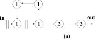
As explained in [12], unlike repipelining, C-slow retiming can enhance designs that contain feedback loops. C-slowing enhances retiming simply by replacing every register with a sequence of C separate registers before retiming occurs; the resulting design operates on C distinct execution tasks. Because all registers are duplicated, the computation proceeds in a round-robin fashion, as illustrated in Fig.6. In this example, this is 2-slow, the design interleaves between two computations. On the first clock cycle, it accepts the first input for the first stream of execution. On the second clock cycle, it accepts the first input for the second stream, and on the third it accepts the second input for thefirst stream. Because of the interleaved nature of the design, the two streams of execution will never interfere. On odd clock cycles, thefirst stream of execution accepts input; on even clock cycles, the second stream accepts input.
in 1 1 out
(b)
Figure.8: converted to 2-slow operation (a), The design retimed (b).
The example from Fig.8, converted to 2-slow operation (a). The critical path remains unchanged, but the design now operates on two independent streams in a round-robin fashion. The design retimed (b). By taking advantage of the extraflip -flops, the crit ical path has been reduced from 5 to 2. In this paper, we designed proposed architecture base on 2-slow retiming and 3-slow retiming. C-slow retiming can be enhanced by designing with feedback loops. Thus we with more registers retiming can break the design into finer pieces until improves throughput total of design. It also enables more throughputs when exploiting task level parallelism. Using C-slow retiming technique in proposed method automatically rebalances the registers in the proposed design, in order to minimize the worst case register to register path. Fig.9 shows the proposed architecture for 2-slow retiming.
RF1
Figure.9: Proposed architecture for 2-slow retiming
Also Fig.10 shows the proposed architecture for 3-slow retiming.
RF1
Figure.10: Proposed architecture for 3-slow retiming.
-
C. Double Edge Triggered Registers
One of the reasons using double edge register is reducing power consumption. Thus we in proposed datapath transition of data that are in two edge clock signal i.e. we reduce the operation frequency to half but without reducing efficiency. As explained in [13], a digital system, synchronization/clocking has its special role. By its action as timing signal the system clock controls the working rhythm of the chip. If the system is considered as a set of interconnected gates and flip-flops, the clock signal controls all flip-flops to sample and store their input data synchronously. In addition, to distribute the clock and control the clock skew, one needs to construct a clock network with clock buffers. Recent studies indicate that the clock signals in digital computers consume a large (15% - 45%) percentage of the system power [14]. In the stored state, the clock level switches off the input path, and, the input data are thus rejected, while the input state, the clock level allows the input signal to travel to the output terminal of the latch. However, if the input date can be received and sampled at both levels of the clock, the flip-flop will receive and process two data values in one clock period. In other words, the clock frequency could be reduced by half while keeping the data rate the same. This means that under the requirement of preserving the original circuit function and data rate, the dynamic power dissipation due to clock transitions can be reduced by half. It is expected that the half-frequency reduced clock system is useful in low power systems. The latch is the basic unit for composing a flip-flop. The levels of a clock, CLK, are used to drive the latch to either the storage state or the input state. If we use D, Q and Q’ to express the input signal, present state and next state of a latch, the state equations for positive and negative level-sensitive latch can be expressed as:
Q '= D.CLK + Q.CLK (2)
Q '= D.CLK + Q.CLK (3)
Equation (2) describes a latch which passes the input data when CLK = 1 and stores it when CLK = 0. Inversely, equation (3) describes a complementary latch, which receives input data at CLK = 0 and stores it at CLK = 1. The corresponding logic structures can be realized with a MUX, as shown in Fig.9(a). If two complementary latches are connected in series, one will be in the storage state while another is in the input state and a “non-transparent” edge triggered flip-flop is formed. Taking the latches in Fig.11 (a), they can compose a well known “master-slave flip-flop” as shown in Fig.11 (b), when CLK = 1, its master latch passes input data and its slave latch is in the storage state; when CLK = 0, its master latch will be in the storage state and its slave latch will pass and output the signal stored by the master latch. Therefore, this flip-flop changes its state at the clock’s falling edge and keeps its state unchanged on the clock’s rising edge. The master latch does not receive the input data when CLK = 0. Obviously, if the input data has to be received at both clock levels, these two complementary latches should be connected in parallel rather than in series. Then obtain a “side-by-side flip-flop” as shown in Fig.11 (c). Since the flip-flop is required to be non transparent from input to output, the output terminal should always be connected to the latch which is in storage state. Because the flipflop’s state can change at both falling and rising edges of the clock, it is named “Double-Edge-Triggered FlipFlop” and is denoted by the legend shown in Fig.11 (c).
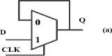
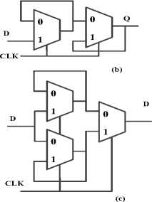
Figure.11: Positive level-sensitive latch (a), SET flip-flop (b), DET flip-flop (c).
The proposed double edge register is shown in Fig.12.
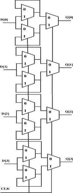
Figure 12: Proposed double edge register.
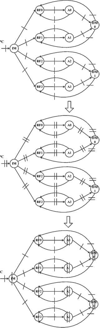
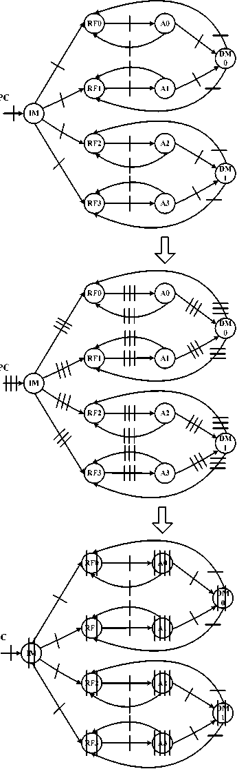
We increase system throughput by applying parallel streams of execution to operate simultaneously. Additional to data processing with parallel execution path, we use several techniques. The ideal goal of all these methods is to increase architecture throughput by operating on multipath streams of execution in highly complex designs, including microprocessors. The proposed microarchitecture is shown in Fig.13. Total of methods are applied to the MIPS processor. As seen in Fig.13 microarchitecture is divided into two interacting parts: the data path and the control. The datapath operates on words of data. It contains structures such as memories, registers, ALUs, and multiplexers. The microarchitecture includes 4 level parallelism.
Control Unit
Figure 13: Proposed microarchitecture.
We use a demaltiplexer 1 to 4, That is after instruction memory and based on bits 33:32 of the instructions. Proposed instruction is shown in below:
Bits 33:31 (I 33:32 ) are for selecting one of level parallelism. As seen in Table II if bits of 33:32 be ‘00’ level0 is selected, if I33:32 = ‘01’ level1 is selected, if I33:32 = ‘10’ level2 is selected and also I33:32 = ‘11’ level3 is selected.
Table I: Bits 33:31of instruction in proposed architecture.
|
I 33:32 |
Level of parallelism |
|
‘00’ |
Level 0 |
|
‘01’ |
Level 1 |
|
‘10’ |
Level 2 |
|
‘11’ |
Level1 |
Structure of instruction is shown in Fig 14(a), for example, an addition instruction (a = b + c) that is in the level 0 format of this instruction is in Fig 14 (b):
Bit[33:32] Bit[31:0]
Level[0 to 3]
Other bits
(a)
|
Level[0] |
Oprand(add) |
a |
b |
c |
(b)
Figure 14: (a) Structure of instruction in the proposed method. (b) level0 format of instruction (a = b + c).
The proposed microarchitecture is a 34-bit architecture, so its a 34-bit data path. The control unit receives the current instruction from the data path and tells the datapath how to execute that instruction. Specifically, the control unit produces multiplexer select, and memory writes signals to control the operation of the data path. The program counter register contains the address of the instruction to execute in one of the levels. The PC is an ordinary 32-bit register. Its output, PC, points to the current instruction. We begin constructing the datapath by connecting the state elements with combinational logic that can execute the various instructions in ALUs we also use high speed digital circuits for adders and multiplier. Control signals determine which specific instruction is carried out by the data path at any given time. The controller contains combinational logic that generates the appropriate control signals based on the current instruction proposed control unit that is based on logic gates. The proposed datapath is formed by: 4 parallelism level, C-slow retiming with applied double edge registers (dash line demonstrated in microarchitecture), demaltiplexer 1 to 4 for selecting any one of level parallelism, this principle of enhancing the datapath’s capabilities is extremely useful, one multiplexer 4 to 1 to choose inputs from several possibilities which is for selecting next instruction or branch instruction, and in the proposed microarchitecture (we) instead of one port RAM for Data Memory we use one Dual Port RAM(DPRAM) for any two level parallelism thus two DPRAM are use in total of the proposed architecture.
-
IV. Comparison
This paper presents a novel high performance and low power microprocessor based on MIPS processor on FPGA for high speed applications. In this paper for verification MIPS processor is chosen as a benchmark for test applied methods. The proposed method has better performance than a traditional MIPS processor. The proposed method has been written with VHDL hardware description language. In order to get actual numbers for the hardware usage and maximum operation frequency this work was synthesized and implemented using Quartus II 9.1V software. Table II shows logic utilization (number of registers, combinational ALUTs, total block Memory bits) and maximum frequency in traditional MIPS (MIPS_only), pipelined traditional MIPS with one edge register (MIPS_pipe), the proposed architecture with one edge register(method_1), and proposed architecture with a double edge register(method_2).
Table II: Logic utilization and maximum frequency in different implementation.
|
Impleme ntation |
Device |
ALUTs |
Regs |
Memory bits |
F Max ( MHz) |
|
MIPS_on ly |
EP2S15 F484C3 |
109 |
2 |
640 |
184.6 4 |
|
MIPS_pi pe |
EP2S15 F484C3 |
265 |
772 |
2560 |
296.8 2 |
|
Method_ 1 |
EP2S15 F484C3 |
776 |
1176 |
2896 |
401.6 5 |
|
Method_ 2 |
EP2S15 F484C3 |
2438 |
102 |
832 |
252.1 1 |
Table III shows the power consumption in methd_1 and method_2. Power is analyzed using the Xilinx XPower analyzer. XPower is the power analysis software available for programmable logic design. It enables to interactively and automatically analyze power consumption for Xilinx FPGA and CPLD devices. XPower includes both interactive and batch applications. Earlier in the design flow than ever, the total device power, power per-net, routed, partially routed or unrouted designs can be analyzed. The achieved results of applied the proposed method to MIPS processor show that a low power and fast architecture have been achieved successfully.
Table III: Power consumption.
|
Clock |
Device |
Power_method_1 (mW) |
Power_method_2 (mW) |
|
100MH z |
Xc4vfx100 |
200 |
167 |
|
75MHz |
Xc4vfx100 |
158 |
133 |
|
50MHz |
Xc4vfx100 |
116 |
96 |
|
25MHz |
Xc4vfx100 |
74 |
58 |
As seen in the two above Tables maximum frequency is increased in method_1 (the proposed architecture with one edge register) and power consumption of the proposed method with a double edge register (method_2) is decreased.
-
V. CONCLUSION
The aim of this paper is to develop implementation an FPGA based novel modified high performance and low power microprocessor. Proposed methods applied to increase performance and reduce power consumption of the designed architecture included, unfolding transformation (parallel processing), C-slow retiming, and also with using a double edge register. The main ideal goal of all these methods is to increase architecture throughput by reduce execution time in highly complex designs including microprocessor. The achieved results ensure verification of the proposed microarchitecture on high-speed FPGA.
References Design and Development MIPS Processor Based on a High Performance and Low Power Architecture on FPGA
- Weng Fook Lee, “VLIW Microprocessor Hardware Design for ASIC and FPGA”, McGraw-Hill Professional; 1, edition (28 Aug 2007).
- David Money Harris, Sarah L. Harris, “Digital Design And Computer Architecture”, published by Elsevier Morgan Kaufmann March 16, 2007.
- Shum, C.-L. K.; Busaba, F.; Dao-Trong, S.; Gerwig, G.; Jacobi, C.; Koehler, T.; Pfeffer, E.; Prasky, B. R.; Rell, J. G.; Tsai, A.c, “Design and microarchitecture of the IBM System z10 microprocessor”, IBM Journal of Research and Development , Volume: 53 , Issue: 1 , pp. 1 - 12, 2009.
- Qu Wenxin; Fan Xiaoya; Hu Ying, “32-bit High Performance Embedded Microprocessor”, Electronic Measurement and Instruments. ICEMI '07. 8th IEEE International Conference , pp. 196 – 198, 2007.
- Slaton, J.; Licht, S.P.; Alexander, M.; Reeves, S.; Jessani, R.; Kishore, K.R., ., “The PowerPC 603e microprocessor: an enhanced, low-power, superscalar microprocessor”, Computer Design: VLSI in Computers and Processors. ICCD '95. Proceedings., IEEE International Conference , pp. 196 – 203, 1995.
- Hlophe, H.B.; Chatelain, D.; van Wyk, B.J. “DOTTA: a dynamic VLIW like microprocessor framework for high speed parallel computing ”, AFRICON, 2004. 7th IEEE AFRICON Conference in Africa, pp. 557 – 562, Vol.1, 2004.
- R. De J. Romero-Troncoso; A. Ordaz-Moreno; J. A. Vite-Frias; A. Garcia-Perez, “8-bit CISC Microprocessor Core for Teaching Applications in the Digital Systems Laboratory”,Reconfigurable Computing and FPGA's, Reonfig. IEEE, pp.1 – 5, 2006.
- Joaquín Olivares, José Manuel Palomares, José Manuel Soto, Juan Carlos Gámez, “Teaching Microprocessors Design Using FPGAs”, Education Engineering (EDUCON), 2010 IEEE, 14-16 April 2010, pp. 1189 - 1193 .
- Skobla, J. , “A novel approach to teaching microprocessor design using FPGA and hierarchical structure”, Microelectronic Systems Education. MSE '09. IEEE International Conferencen , pp. 111 – 114, 2009.
- Bryan H. Fletcher, “FPGA Embedded Processors: Revealing True System Performance”, Embedded Systems Conference San Francisco 2005 ETP-367.
- O. Shoewu and O.T. Baruwa, “Design of a Microprocessor Based Automatic Gate” The Pacific Journal of Science and Technology , Volume 7. Number 1. May 2006 (Spring), pp. 31-44.
- Scott Hauck and Andr´e DeHon, “Reconfigurable Computing The Theory And Practice Of FPGA-Basedcomputation”, Elsevier Morgan Kaufmann Series in Systems on Silicon, 2008.
- Massoud Pedram, Qing Wu, Xunwei Wu, “A New Design for Double Edge Triggered Flip-flops”, Design Automation Conference 1998. Proceedings of the ASP-DAC '98. Asia and South Pacific, pp. 417-421.
- G. E. Tellez, A. Farrah and M. Sarrafzadeh, “Activity-driven clock design for low power circuits,” in Proc. IEEE ICCAD, San Jose, pp.62-65, Nov. 1995.
