Design and implementation of a novel complete filter for EEG application on FPGA

Author: Atik Mahabub
Journal: International Journal of Image, Graphics and Signal Processing @ijigsp
Article in issue: 6 vol.10, 2018.
Free access
Filter is vastly used to detect different human signal in real time. In this paper, a novel complete digital filter is proposed for the fast detection of EEG signals due to avoid the mixtures of different biomedical signals. This paper intends to design a digital complete filter based on Field Programmable Gate Array (FPGA) for the alleviation of unwanted frequency components in biomedical signals specially EEG signals. For this purpose, complete filter which is a combination of integrator filter and differentiator filter which supports both low and high noises and comparatively inexpensive than other signal processing methodologies can be used. For hardware implementation, FPGA board is used which is a combination of different logic gates which offers inexpensive and long lasting services.
Filter, FPGA, RTL, Floor plan, EEG signal, Timing diagram
Short address: https://sciup.org/15015969
IDR: 15015969 | DOI: 10.5815/ijigsp.2018.06.03
Text of the scientific article Design and implementation of a novel complete filter for EEG application on FPGA
Published Online June 2018 in MECS DOI: 10.5815/ijigsp.2018.06.03
An electroencephalogram is a type of signal which is very low in strength. The power ranges from150 to 290 microvolts. These signals originated from the human brain are the graphical sketch of the brain activity. In the frequency domain, there is a scaling from 0.5 Hz to 100 Hz. And this specific scaling totally belongs to the frequency nature of electroencephalogram signals.
Now as a matter of fact, in this is study we are trying to stretch our time and implemented it to design an experimental model for detecting electroencephalogram signal. But from the past we can assure, detection of the EEG signal is not an easy task. Moreover, research associated with designing a hardware structure for detecting and analyzing EEG signal indicating that it is a quiet Complex work. Hence it is a non-stationary signal but its power spectral analysis is quite valuable. We can acquire not only the statistical analysis of the signal from the spectral estimating graph but also the characteristic summary.
Spectral analysis of electroencephalogram signal has been observed for the first time through computers during 1963 by Walter. But mankind was unable to use this variable analysis for 2 years. During 1965 we have witnessed the introduction of the fast Fourier transform and for the first time signal analyzing has become much easier than ever although at that time it can only measure 8 seconds of data at a time.
Although fast Fourier transform is a means for analyzing the complex signal in an efficient way but it is not the only way. So these papers have proposed a different method apart from FFT which is known as stochastic measurements [1, 2], instead of spectral analysis they have shown their affinity with voltage and current harmonic analysis. In this study [3] they have designed the parameter of stochastic analysis with harmonic estimation for the direct current portion and being converged until 49 harmonics.
In this study, they have shown a different way of [4] analyzing Electroencephalogram signal. The core theme of their study is simply divide and conquer approach. Following these approaches, they have divided the signal into many independent components and they have conducted an independent component analysis approach for this study all over those components. It is proven to be very powerful solve a blind source separation case. However, this case for the clinical source or any high-performance data analysis is not that suitable for low memory and low processor. That’s why this type of operation like to be processed on the online server. But there is also a pitfall for this type of operation these operations may run faster and smoother in the online operational area but they do cost too much computational cost which is not very desirable for any personal or industrial case. The advantages of this study are they can maximize is the data flow, large-scale operation, and efficient data classification. For brain-computer interface [5] this work maybe one of the most notable work ever done. TOP design paradigm for connecting the brain with the computer through that page in a very cheapest way. According to the claim of the authors, they have quoted that to the best of their knowledge this work is the first field Programmable Gate array model for interfacing the brain to with the computer in a cheap way. They have used three different electrodes, as an amplifier and a Field Programmable Gate array which can process a single electroencephalogram signal at a time. The performance of this system is quite satisfactory, the accuracy of processing signal was 92%. The work done by these authors is very compelling and the amount of the accuracy conquered buy them is 96%. They have presented a meticulous field Programmable Gate array platform for processing the pre-defined features of the electroencephalogram signal. And this system is configurable brain-computer interface. They can also filter the input signal; noise removal is also possible as well as baseline analysis. Moreover, linear and nonlinear, univariate, bivariate measuring is also possible through this system.
Chandrakasan and J. Kwong [7] have developed a biomedical signal processing platform which is beginning with a 16-bit microcontroller and ends with accelerators. Their SoC is programmable and also have a dynamic memory which is efficient for estimating and comparing the different length of EEG signals.
They have developed a low-power SoC [8] monitoring system for the continuous electroencephalogram signal also they can perform season deduction through this system. They have used 7 frequency bands also a bank of band-pass filters. For the user, they have managed up to 18 channel facilities.
A proposed diagram is shown in fig. 1 for hardware implementation of digital filter on FPGA circuit boards where analog input amplified EEG signal is converted into digital data stream by using ADC converter then the digital data is reconverted into filtering process and amplified analog signal by using DAC converter is received at the output end. This paper represents a simple filter for EEG signal which would help to differentiate the filter with other human signal like EMG, ECG, EOG etc. It is a low-cost filter using only registers and needs less space and power for implementation. The system uses a computer in which the design can be programmed and simulated on Quartus II software with interface to ALTRA Cyclone DE II board of FPGA device. From the implementation side, references [9 - 11], use Altera devices.
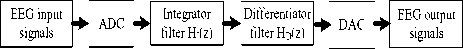
Fig.1. Basic block diagram of getting EEG signal by complete filter.
We have organized this study in 4 steps. The first step is associated with the discussion of the background of the complete filter. The second step is discussing the architectural analysis of this proposed methodology for the FPGA. The third state is containing of results and analysis of different portions of the result. The final stage is consisted of the conclusions and future work of the study.
-
II. Background
Consider a recursive and no recursive N-point digital filters, with the basic building block structure in Figure 2, are characterized by the following difference equation:
y int (n) - d o %(n) + Ь о у(п — 1) (1)
У^) - C o vin') — d o y(n — 1) (2)
Where x(n) represents the latest input sample, x(n — 1) the last sample, and ylnt (n) is the integrator filter output data sequence, y(n) is the output data sequence of the system and y(n — 1) is previous output of the system. The parameters a0, b0, Co and d0 are the filter coefficients. If the coefficients a0 — 1, b0 — 1 , Co = 1 and d0 — 1 then the proposed filter equation will be:
V n U) = x(n) + y(n — 1) (3)
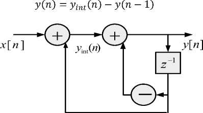
Fig.2. Proposed realization structure of complete filter.
The equation (3) is called transfer function of the integrator. An integrator filter is a digital high pass filter (HPF). Basically, the integrator circuit is similar to an accumulator which is used to accumulate or store the sum of the input data.
Taking Z-transform on both side of the equation (1) as yint(n) - X^) + y(n — 1) Y(z) — X(z) + z-1Y(z) Y(z) — z-1Y(z) = X(z) Y(z)(1 — z-1) = X(z)
Y(z) _ 1
nt n t(z)-^- (i-;-r)
H [ nt(z') Represents the transfer function of the Z-transform. The output of the integrator is the sum of the present input and the past output as can be observed from the time domain representation the equation (3) based on the equation (5), a block diagrammatic representation of the digital integrator can be modeled and is shown in Figure 3.
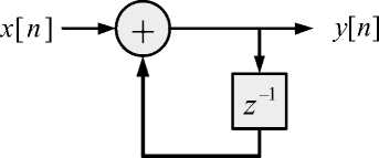
Fig.3. Block diagram of a digital integrator
In the equation (4) is also used time-domain transfer function of differentiator. A differentiator filter is a digital low pass filter (LPF). The time domain and the transfer function of the differentiator are given as:
y(n) - x(n) — x(n — 1)
Taking Z-transform on both side of the equation (4) as
Y(z)=X(z) — z 1X(z) Y(z) = X(z)(1 — z-1) H(z)=^g=1-z-1
From the time domain representation of it can be explained that the output of the differentiator is the difference between the present input and the past input. Based on the equation (6) the block diagram of the differentiator can be modeled and is shown in Figure 4.
the coefficients and data are accessed sequentially from memory and applied to the register and multiplied. The products are summed in the accumulator. Successive multiplication-accumulation (MAC) will be performed.
x [ n ]
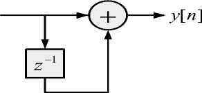
Fig.4. Block diagram of a digital differentiator.
-
III. Proposed Algorithm
-
1) Initialization: Initialize system, this may include setting up a coefficient table.
-
2) Input section: this may include reading of the input sample, x(.), e.g. from an ADC via a serial port.
-
3) Inner loop computation: The execution of the proposed difference equation of the digital filter equation (1) & (2) to obtain y(n).
-
4) Output section: This may include
shifting/rounding of the result of the inner loop computation and sending this, e.g. to the DAC via a serial port.
As much of steps, 1, 2 and 4 are the system dependent, we will concentrate on the inner loop computation here. The proposed digital filter inner loop may be implemented with the following instruction in ALTRA Cyclone II board with processors EP2C35F672C.
The coefficients, ak, bk and the data array are stored in memory as shown in Figure 3 & 4. In the pipeline mode,
-
a. Adds the previous product to the accumulator e.g. initially, the product is zero.
-
b. Multiply the coefficients ak by the data memory x(n) and store into AR1 and also bk by y(n — 1) and store into AR2, initially AR1 point’s x(n) and then successively, points x(n — N) decrement the address by 1 and initially AR2 points y(. — 1) and successively, points y(. — N + 1) as we go round the loop.
-
c. Adding the data from AR1 and AR2 and store into AR3, which is represent y£nt(n).
-
d. Multiply the coefficients ck to auxiliary register AR3 store into AR4 and Multiply the coefficients dk to auxiliary register AR2 store into AR5. Initially AR4 point’s y t n t (.) and then
successively, points y£nt(n — N) decrement the address by 1 and initially AR5 points y(. — 1) and successively, points y(. — N + 1) as we go round the loop.
-
e. Decrements AR4 by AR5 and store into AR6 which represents y(.).
Coefficient
memory
a 0
aN
Register
Coefficient
Coefficient
Data
Data memory memory memory memory
|
x ( n ) |
b 0 |
y ( n - 1) |
d 0 |
|||
|
Xn - N + 1) |
b N |
y(n - N) |
dN |
Register
Register
Register
Multi lier
Coefficient
c 0
c
Register
M tiplier
Multiplier
+
Register
JinO
y ,nt( n - N
Register
Multiplier
Register
Register
y ( n )
Fig.5. Pipelined MAC configuration of Integrator filter Hint and Differentiator filter Hdi ff which make this complete filter.
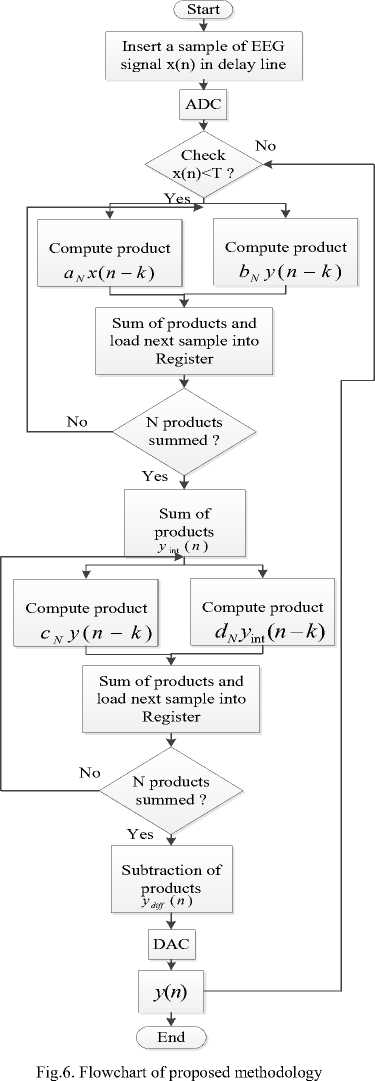
Figure 7 it is seen that, at the Ith cycle, the processor could be simultaneously fetching the Ith instruction, decoding the (i — 1)th instruction and at the same time executing the (i — 2)th instruction.
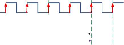
Figure 8 giving the timing diagram for a three-stage pipeline, draw to highlight the instruction steps. Typically, each step in the pipeline takes one machine cycle. Thus during a giving cycle up to a three different instructionsmay be active at the same time, although each will be at a difference stage of completion. The key to an instructions pipeline is that the three parts of the instructions are independent and so the execution of multiple instructions can’t be overlapped. Here differentiator output is the main output of the proposed filter.
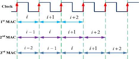
Fig.7. Timing diagram for a pipelined MAC unit.
Clock
1st MAC
2ndMAC
Read
x (0)
y int(0)
Read
x (1)
y int (1)
Read
x (2)
Integrator filter
Differentitor filter
Differentitor filter
Differentitor filter
y (1)
Integrator filter
y (2)
Integrator filter yint(2) y(3)
3rd MAC
Fig.8. Timing diagram for a pipelined MAC unit for the proposed filter
-
IV. Description of Different RTL Blocks
Register-transfer-level (RTL) abstraction is used in hardware description languages (HDLs) like Verilog and VHDL to create high-level representations of a circuit, from which lower-level representations and ultimately actual wiring can be derived. Design at the RTL level is typical practice in modern digital design [12]. Here, Verilog hardware description language has been used for RTL designing. The description of different RTL blocks has been given below:
-
A. Data_in
It is a register type module which temporarily stores the input EEG signal value and it serves this value to the Buffer in accordance to the control ROM bit sequences. It is an 8-bit register.
-
B. Data_out
It is also a register type module which temporarily store the values from Buffer and provides it to the peripherals of the system. It is an 8-bit register.
-
C. Clk
Clk is used to send pulses to the flip-flops. It is a single bit register. It helps to count cycles and data can be passes through registers.
-
D. Hold
It is a single bit register which helps to see some specific data of EEG signal or to stop that data so that the data can be monitored if unwanted something happen and to halt the other data.
-
E. Reset
It is a single bit register which used to set the value of data to an initial stage and refresh the ROM memory. Reset is used at the start of every new process.
-
F. LESS_THAN
It is used give a threshold value so that below or above of this threshold value data can’t pass through the MUX21 and go for the loop procedure.
-
G. Buffer
It is a one kind of register which temporary store the data after the process of clk, reset and hold when the data is entered from the Data_In. It is an 8-bit register.
-
H. Add0
It is a register type module used to add data as a function of an integrator filter which is described in equation 3.
-
I. Add1
It is also a register type module used to subtract data as a function of a differentiator filter which is described in equation 4 and passes the data to output stage which is named ‘Data out’.
-
J. MUX21
There are 6 MUX21 in the RTL. Three are for Data_In and three are for Data_out. All of them are 8-bit registers which temporary store the data after the input and before the output procedure.
Figure 9 and 10 describe RTL and past RTL diagram of the complete filter respectively.
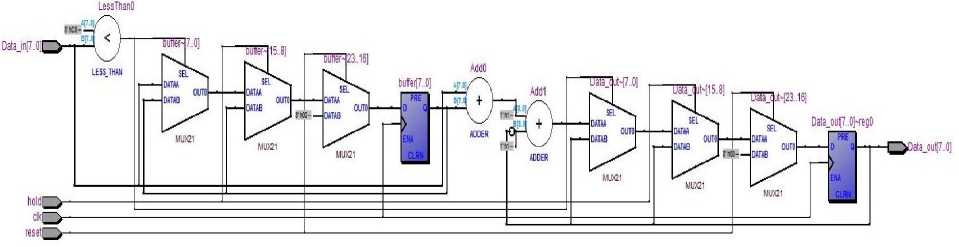
Fig.9. RTL diagram of the proposed model
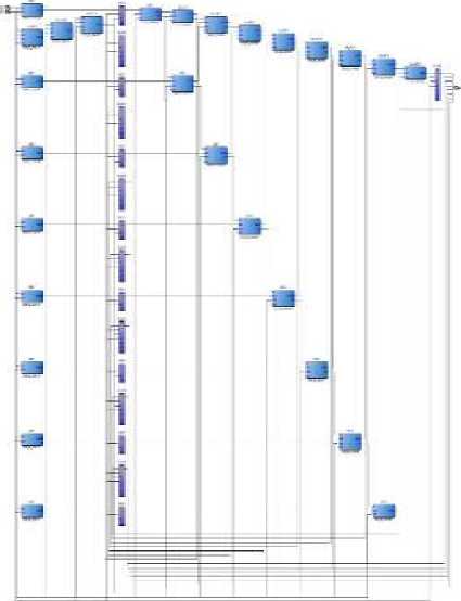
Fig.10. Post RTL diagram of the proposed model
Floor plan indicates that the area required by the synthesized circuit is very small which can be observed from the chip planner view of ALTRA Cyclone II board with processors EP2C35F672C6 as given in Fig. 11. The chip planner view shows the placement and amount of the CLBs to implement the design inside the FPGA chip [13]. Figure 11 shows that the area occupied by the synthesized circuit (area occupied by rectangles bluer than the others) is quite small.
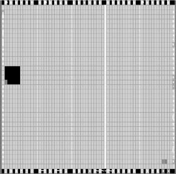
Fig.11. Floor plan of the proposed model
-
V. Result Analysis
These coefficients are fed from an ADC. The first things to do is to allocate two sets of contiguous memory locations (in RAM), one for storing input data (x(n),x(n — 1),y(n — 1),y(n)), and the other for the filter coefficients (a0 = 1, b0 = 1, c0 = 1 and d0 = 1) as depicted below:
|
Data in RAM |
Coefficient Memory |
|
0 |
a0 = 1 |
|
0 |
b 0 = 1 |
|
0 |
c0 = 1 |
|
0 |
d 0 = 1 |
At initialization, the RAM locations where the data samples are to be stored are set to zero since we always start with no data. The following operations are then performed.
Step. 1: Read EEG data sample from EEG database to the ADC after threshold applied, shift data RAM one place (to make room for the new data), save the new input sample, compute integrator output sample from Equation (3) and compute final output from Equation (4) and then send to the DAC: At initial stage, setting first positive clock pulse=1, reset=1, hold=0, and initial past sample output: y(—1) = 0 (computed output samples as shown in Table. 1)
|
Data in RAM |
Coefficient Memory |
Difference Equation |
|
x(0) = 0 |
1 |
|
|
x(0) = 0 |
1 |
|
|
y^tOT = 0 |
1 |
y tnr (0) = x(0) + y(—1) = 0 |
|
y(0) = 0 |
1 |
y(0) = y^tTO — y(n — 1) = 0 |
Step. 2: Repeat the above operation at 2nd positive clock pulse=1, reset=0, hold=0 and workout the new output sample and send to the DAC:
|
Data in RAM |
Coefficient Memory |
Difference Equation |
|
x(0) = 0 |
1 |
|
|
x(1) = 60 |
1 |
|
|
y™ t (1) = 60 |
1 |
УшгШ = x(1) + y(0) = 60 |
|
y(1) = 60 |
1 |
y(1) = y™ t (1) — y(0) = 60 |
Step. 3: Repeat the above operation at 3rd positive clock pulse=1, reset=0, hold=0 and workout the new output sample and send to the DAC:
|
Data in RAM |
Coefficient Memory |
Difference Equation |
|
x(1) = 60 |
1 |
|
|
x(2) = 46 |
1 |
|
|
У™г(2) = 106 |
1 |
y(nt(2) = x(2) + y(1) = 106 |
|
y(2) = 46 |
1 |
y(2) = y(nt(2) — y(1) = 46 |
Step. 4: Repeat the above operation at 4th positive clock pulse=1, reset=0, hold=0 and workout the new output sample and send to the DAC:
|
Data in RAM |
Coefficient Memory |
Difference Equation |
|
x(2) = 46 |
1 |
|
|
x(3) = 38 |
1 |
|
|
У™г(3) = 84 |
1 |
y™ t (3) = x(3) + y(2) = 84 |
|
y(3) = 38 |
1 |
y(3) = yint(3) —y(2) = 38 |
Step. 8: Repeat the above operation at 8th positive clock pulse=1, reset=0, hold=1 and workout the new output sample and send to the DAC:
|
Data in RAM |
Coefficient Memory |
Difference Equation |
|
x(6) = 28 |
1 |
|
|
x(7) = 30 |
1 |
|
|
У™ г (7) = 58 |
1 |
y ,„, (7) = x(7) + y(6) = 58 |
|
y(7) = 28 |
1 |
y(7) = yint(7) — y(6) = 28 |
Note that the oldest data sample has now fallen off at the end. Step. N: Repeat the above operation at nth positive clock pulse=1, reset=0, hold=0 , past sample output: y(n — 1) and workout the new output sample and send to the DAC:
|
Data in RAM |
Co-efficient Memory |
Difference Equation |
|
x(n — 1) = N — 1 |
1 |
|
|
x(n) = N |
1 |
|
|
У» с (п) = x(n) — x(n— 1) |
1 |
yint(n) = x(n) +y(n — 1) |
|
y(n) = N — 1 |
1 |
y(3) = yint(n) — y(n — 1) |
Table 1 shows the comparisons between input and output data of the proposed filter. The input data is the EEG signal, integrator output is the output of the integrator filter, hold is used for to see a specific data, output (quantized) is the original output data of the proposed filter which is the EEG signal as shown in the equation 2.
Table 1. Example of EEG data and corresponding filtered output data
|
clk* 2 |
Reset |
Hold |
Input |
Integrator Output |
Output |
Output (without hold) |
|
0->1 |
1 |
0 |
0 |
0 |
0 |
0 |
|
0->1 |
0 |
0 |
60 |
60 |
60 |
60 |
|
0->1 |
0 |
0 |
46 |
106 |
46 |
46 |
|
0->1 |
0 |
0 |
38 |
84 |
38 |
38 |
|
0->1 |
0 |
0 |
29 |
67 |
29 |
29 |
|
0->1 |
0 |
0 |
28 |
57 |
28 |
28 |
|
0->1 |
0 |
1 |
30 |
58 |
28 |
30 |
|
0->1 |
0 |
0 |
28 |
58 |
28 |
28 |
|
0->1 |
0 |
0 |
30 |
58 |
30 |
30 |
|
0->1 |
0 |
0 |
36 |
66 |
36 |
36 |
|
0->1 |
0 |
0 |
51 |
86 |
51 |
51 |
|
0->1 |
0 |
1 |
53 |
104 |
51 |
53 |
|
0->1 |
0 |
0 |
62 |
115 |
62 |
62 |
|
0->1 |
0 |
0 |
65 |
127 |
65 |
65 |
|
0->1 |
0 |
0 |
69 |
134 |
69 |
69 |
|
0->1 |
0 |
0 |
72 |
141 |
72 |
72 |
|
0->1 |
0 |
1 |
79 |
151 |
72 |
79 |
|
0->1 |
0 |
0 |
82 |
161 |
82 |
82 |
|
0->1 |
0 |
0 |
79 |
161 |
79 |
79 |
Figure 12 shows the comparison chart among input, output and integrator output data where x-axis shows the quantized value of EEG signal and y-axis shows the no. of data. This chart is made on the basis of 180 data.
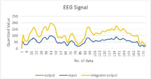
Fig.12. Comparison chart among input, output and integrator output data of EEG signal
(a)
(b)
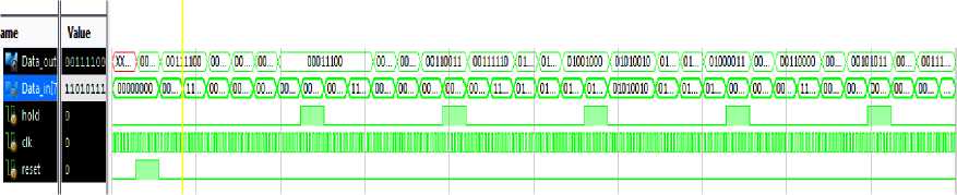
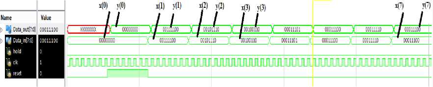
Fig.13. Timing diagram of (a) real time EEG signal data (b) specified 7 data of proposed filter
Figure 13 shows the real time result analysis of EEG signal with the help of this proposed complete filter. Here 60 is the input value whose binary value is 00111100 because input data is 8 bits. After solving with complete filter, the binary integrator output value is 00111100 in decimal 60 as the initial value is zero and the last output value is 00111100 in decimal 60. The output will store to the memory RAM as previous output value. Here 46 is the input value whose binary value is 00101110 because input data is 8 bits. After solving with complete filter, the binary integrator output value is 01101010 in decimal 106 as previous value is 60 and the last output value is 00101110 in decimal 46 as desired. The output will store to the memory RAM as previous output value. After following the closed loop, the output values for different values of input are shown in Fig. 13 which represent the timing diagram of the proposed filter.
FPGAs are pre-fabricated semiconductor device which consist of different number of interconnected reconfigurable logic elements and each element consist of a number of blocks. It consists of high speed lOBs , LUT, flip-flop and memory blocks, has CLB with multiple slices and DSP blocks [14,15]. The ALTRA Cyclone II board with processors EP2C35F672C6 is used for implementing our proposed architecture. Table. 2 shows the device utilization summary and timing summary. The total device utilization of the proposed design is less than one percent.
-
VI. Conclusions
Though there are many filters are available, complete filter can become one of the best and mostly used filters for the detection of EEG signal. By using FPGAs, this paper implemented a filter digitally. FPGAs are more useful than any other digital system and using Verilog HDL exact synthesized result and RTL schematic has been established. Less blocks were used with very little delay. The proposed method is low cost, high performance, self-reconfigurable, flexible and easy to implement. This proposed architecture can be useful for real time EEG signal detection application. In future, this proposal can be designed and implemented for other biomedical signals to make it more effective.
Table 2. Shows the device utilization summary, power and timing summary
|
Name |
Device Utilization |
|
|
Used |
Percentage |
|
|
Total logic elements |
27 / 33,216 |
< 1 % |
|
Dedicated logic registers |
16 / 33,216 |
< 1 % |
|
Total LABs: partially or completely used |
2 / 2,076 |
< 1 % |
|
I/O pins |
18 / 475 |
4 % |
|
Clock pins |
5 / 8 |
63 % |
|
Block interconnects |
44 / 94,460 |
< 1 % |
|
C16 interconnects |
8 / 3,315 |
< 1 % |
|
C4 interconnects |
26 / 60,840 |
< 1 % |
|
Direct links |
16 / 94,460 |
< 1 % |
|
Local interconnects |
17 / 33,216 |
< 1 % |
|
R24 interconnects |
8 / 3,091 |
< 1 % |
|
R4 interconnects |
20 / 81,294 |
< 1 % |
|
LUT 4 inputs |
2 |
|
|
LUT 3 inputs |
15 |
|
|
LUT 2 input |
10 |
|
|
Maximum fan-out |
17 |
|
|
Average fan-out |
2.14 |
|
|
Total fan-out |
137 |
|
|
Nominal Core Voltage |
1.2 V |
|
|
Clock frequency |
10 MHz |
|
|
Bus width |
16 bits |
|
|
Baseline area |
32 LEs |
|
|
Multiplexer Inputs |
3:1 |
|
|
Area If reconstructed |
16 LEs |
|
|
Saving if reconstructed |
16 LEs |
|
|
Voltage |
3.3 V |
|
|
Minimum input arrival time before clock |
170 psec |
|
|
Maximum input arrival time before clock |
2523 psec |
|
|
Maximum Logic Delay |
7.6 nsec |
|
|
Minimum Logic Delay |
4 nsec |
|
Acknowledgment
References Design and implementation of a novel complete filter for EEG application on FPGA
- V. Vujičić, S. Milovančev, M. Pešaljević, D. Pejić and I. Župunski, "Low frequency stochastic true RMS instrument," IEEE Trans. Instrum. Meas., vol. 48, pp.467-470, Apr. 1999.
- V. Vujičić, “Generalized low frequency stochastic true RMS instrument”, IEEE Trans. Instrum. Meas., vol. 50, pp. 1089-1092, Oct. 2001.
- V. Pjevalica, and V. Vujičić, “Further Generalization of the LowFrequency True-RMS instrument”, IEEE Trans. Instrum. Meas., Revised IM 5499, to be published
- Wei-Chung Huang1, Shao-Hang Hung1, Jen-Feng Chung1,2, Meng-Hsiu Chang1, Lan-Da Van2, and Chin-Teng Lin, " FPGA Implementation of 4-Channel ICA for On-line EEG Signal Separation".
- K. K. Shyu, P. L. Lee, M. H. Lee, M. H. L. R. J. Lai, and Y. J. Chiu, “Development of a low-cost FPGA-based SSVEP BCI multimedia control system,” IEEE Trans. Biomed. Circuits Syst., vol. 4, pp. 125–132, April 2010.
- L.P Wijesinghe*, D.S Wickramasuriya, and Ajith A. Pasqual," A Generalized Preprocessing and Feature Extraction Platform for Scalp EEG Signals on FPGA"
- J. Kwong and A. Chandrakasan, “An energy-efficient biomedical signal processing platform,” IEEE J. Solid-State Circuits, vol. 46, no. 7, pp. 1742–1753, 2011.
- N. Verma, A. Shoeb, J. Bohorquez, J. Dawson, J. Guttag, and A. Chandrakasan, “A micro-power EEG acquisition SoC with integrated feature extraction processor for a chronic seizure detection system,” IEEE J. Solid-State Circuits, vol. 45, no. 4, pp. 804–816, 2010
- C. Chou, S. Mohanakrishnan, and J. B. Evans, “FPGA Implementation of Digital Filters”, Proc. Int. Conf. Signal Proc. Appl. & Tech. (ICSPAT’93),1993.
- J. B. Evans, "Efficient FIR filter architectures suitable for FPGA implementation,"IEEE Transactions on Circuits and Systems II: Analog and Digital Signal Processing, vol. 41, no. 7, pp. 490-493, Jul 1994.
- K. Sundaram, M. Pradeepa, "FPGA based filters for EEG preprocessing," 2016 Second International Conference on Science Technology Engineering and Management (ICONSTEM), Chennai, 2016, pp.572-576.
- Frank Vahid (2010). Digital Design with RTL Design, Verilog and VHDL (2nd ed.). John Wiley and Sons. p. 247. ISBN 978-0-470-53108-2.
- Md. Nazmul Hasan, Md. Tariq Hasan, Rafia Nishat Toma, Md. Maniruzzaman “FPGA Implementation of LBlock Lightweight Block Cipher” Electrical Engineering and Information Communication Technology (ICEEICT), 2016 3rd International Conference on 22-24 Sept. 2016, Dhaka, Bangladesh.
- Shumit Saha, Md. Jahiruzzaman, Chandan Saha, Md. Rubel Hosen, Atiq Mahmud “FPGA Implementation of Modified Type-C PID Control System” in 2nd Int'l Conf on Electrical Engineering and Information & Communication Technology (ICEEICT) 2015 Jahangirnagar University, Dhaka-1342, Bangladesh, 21-23 May 2015.
