Design and Implementation of a Three-operand Multiplier through Carbon Nanotube Technology

Author: Mohammad Reza Reshadinezhad, Niloofar Charmchi, Keivan Navi
Journal: International Journal of Modern Education and Computer Science (IJMECS) @ijmecs
Article in issue: 9 vol.7, 2015.
Free access
Multiplication scheme is one of the most essential factors, which is time consuming. Designers and manufacturers of processors emphasis on methods which would not only perform the multiplication scheme in a rapid manner, but would reduce the physical aspect of the design as well; hence, a reduction in power consumption. Addition is one of the fundamental factors in multiplication. Pre-designing of circuits and transistors' levels used to be made through Metal Oxide Semiconductor Field Effect Transistor (MOSFET), but now, due to scaling and difficulties thereof, new technologies like Single Electron Transistor (SET), Quantum-dot Cellular Automata (QCA) and Carbon Nanotube Field Effect Transistor (CNFET) are introduced. Among the new technologies, CNFET has become center of attention due to similarities in electronic features in relation to MOSFET. A comparison made between CNFET with MOSFET technologies indicate that, power delay product (PDP) and power leakage can be less in nanotube transistors. Field effect transistor circuit's simulations are accomplished through HSPICE simulator. The simulation results indicate that this proposed Three-operand Carbon Nanotube Multiplier has a better performance in comparison with the three-operand multiplication done on computers nowadays, which we call it classical multiplier in this article.
CNFET, Fast Multiplication, Multi-operand Carbon Nanotube Multiplier, Nanotechnology, Partial Product Reduction, Power Leakage
Short address: https://sciup.org/15014794
IDR: 15014794
Text of the scientific article Design and Implementation of a Three-operand Multiplier through Carbon Nanotube Technology
Published Online September 2015 in MECS
In most signal processing procedures, multiplication is applied for calculations such as convolution, filtering, cryptography, residue number system (RNS) and frequency analysis [1, 2, 3]. Therefore, the multipliers can contribute to digital systems design. In different processors architectures the multiplier and adder are considered as the main components of the processors, in a sense that any improvement in their function would lead to an increase in program speed.
In different implementations, in order to evaluate the system efficiency, factors such as power consumption, number and the size of the used transistor and simplicity in design are of essence [4]. Multiplication is an essential operation in computer arithmetic. The multiplication time and the complexity in implementation of which increases as the length of the operands increase in the input of the system. In the arithmetic unit of the processors, multiplication is the main and time consuming operation.
Introducing any method in speeding-up the output result and reduction of the chip size, which would in turn reduce power consumption, would be appreciated by the processor designer. In this respect, applying carbon nanotube technology can be one of the proper manners in fulfilling this objective [5, 6, 7].
CNFETs have their own features and due to their easy implementations have become the center of attention among the researchers in this field. These transistors have a single dimensional unique structure that cause ballistic transport attributes in the nanotube. The P-CNFET and N-CNFET in CNFETs have similar mobility movement and geometric, therefore, a unified currentdrive [8]. The carbon nanotube circuits provide a big chance for the researchers with respect to achieving low power consumption and high speed in comparison with the circuits made of silicone. Lombardi et al. [5] compared MOSFET and CNFET technologies and showed that the power delay product and leakage power in CNFET technology is lower than the MOSFET. In their study, they calculated and compared the leakage power in different base gates and a full adder through CNFET and MOSFET technologies and found that the CNFET has a better efficiency [5].
Multipliers are applied in most of arithmetic systems. Multiplication process is very slow, since a vast number of partial products are added to obtain the final product. Many articles are available on multiplier design [9, 10, 11,
-
12, 13, 14].Multiplication is implemented by
accumulation of partial products, each of which is conceptually produced via multiplying the whole muli-digit multiplicand by a weighted digit of multiplier. Here, we focus on full parallel multiplication, which is generally a 3-step process briefly described below:
-
1) Calculating the partial products, where every partial product is implemented independent of type and processor structure technology with an AND unit. For this purpose many researchers apply the advanced Booth algorithm at this stage, where the number of the partial products is cut in half [11, 15, 16].
-
2) Here, the step is named the reduction stage in a sense that the partial products are converted to the sum vector and the carry vector. In order to
reduce the partial products different methods like the Wallace tree and compressors are adopted [10].
-
3) At this stage a proper carry propagating adder (CPA) is necessary to add the two vectors of the previous stage and generate the final product [4, 17].
In this article a four-bit three-operand carbon nanotube multiplier is presented. The results are compared with the multiplications performed on today’s computer processors, which in this article refers to as classical multiplication. The comparison is in respect to speed, power and power delay product. Up to now, many studies are conducted on multi-operand adders [18]. By applying the multi-operand adders and parallel multiplication scheme and their combination, the author in [19] was able to design and introduce a fast multi-operand multiplier. A three-operand multiplier is presented in [20], which, three methods are introduced for implementation. In the first method, two multipliers are set in series. The first two four-bit operands are multiplied in one another with a product of 8 bit length as the result. This outcome is multiplied in the third operand and the final length of 12 bit is obtained. The partial products are obtained using AND gates. The tree reduction is made through (4:2) compressors. This method is known as the Wallace improvement method where the partial products are reduced to two rows. In the final stage, the product can be obtained through carry propagating adders. Instead of carry propagating adders, a fast adder like carry lookahead adder (CLA) can be used.
In the second method ROM is used for addressing a 256×8 bit memory and then form the lookup table[19, 20].
In the third method all the partial products are generated by using two levels of Booth re-encoding. The first level cuts the partial products in half and in the second level this half is cut in half once more, that is a quarter of the first stage.
Another three-operand multiplier is presented in [21]. They introduced three different methods and the simulations are performed at gate level.
In the reminder of this paper, in section 2 a review of carbon nanotube field effect transistor is presented.
Section 3 includes motivation and a brief description about the classical three-operand multipliers. The proposed CNFET-based three-operand multiplier and the simulation results is presented in section 4. Finally, section 5 concludes the paper.
-
II. Carbon Nanotube And Carbon Nanotube Field Effect Transistors
Carbon nanotube (CNT) is a sheet of graphene (an allotrope of graphite) that is rolled up and shaped a tube.
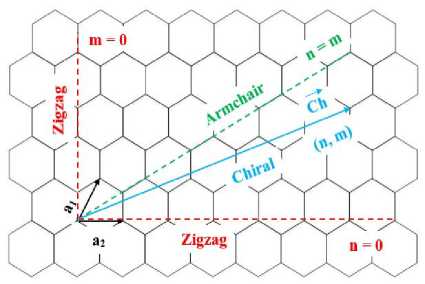
Fig.1. The Graphene Sheet to be Formed in Carbon Nanotube
According to the number of the tubes, CNTs are categorized in Single Walled Carbon Nanotube (SWCNT) and Multi Walled Carbon Nanotube (MWCNT) groups.
Each CNT has a determined vector named chirality, defined as ch = na 1 + ma 2 : where, (n, m) are the chiral numbers and [a 1 , a 2 ] are the unit vectors. According to n and m , the SWCNTs are divided in three types: if m=0 or n=0 , the nanotube resumes zigzag shape, if n=m the CNT resumes the Armchair shape and otherwise, the resumed shape is Chiral. These types are illustrated in Fig. 1. According to the direction of the Chirality vector, the graphene is rolled and the nanotube is made.
The threshold voltage of CNFETs can be controlled by adjusting the nanotube diameteras in (1).
Dcnt = a V n 2 + nm + m 2 = 0.0783 4n 2 + nm + m 2 (1)
n
Where, = √3 is the distance of carbon atoms from one another and = 0.142 nm is a constant number.
It is possible to turn on the CNFET at a required voltage and design the appropriate circuit. The threshold voltage in nanotube is expressed by (2):
v = V3 av n 0.43 v
-
3 eDCNT DCNT
Where, e is the electron charge unit, V π is the π-π bond energy and D CNT is the nanotube diameter. As observed in (2), the transistor threshold voltage have an inverse relation with the CNT diameter. If m is assumed as zero, (3) is introduced for two CNFETs [5, 22, 23]:
Vth 1 DCNT 2 n 2
V th D CNT n 1
The distance between two nanotubes is named Pitch. A CNFET that consists of three nanotubes is shown in Fig. 2(a).
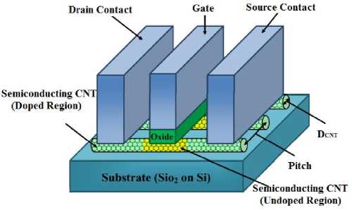
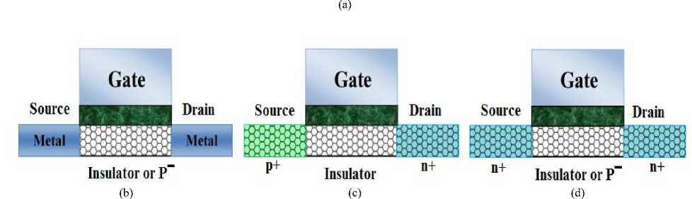
Fig.2. (a) Shematic diagram of Carbon Nanotube Field Effect Transistor, (b) SB-CNFET, (c)T-CNFET, (d) MOSFET-like CNFET [24]
For many years, the designers of integrated circuits adopted MOSFET technology. Researchers concentrated on these transistors type due to their low power consumption and the low hardware circuit manufacturing cost. In order to produce smaller chips, the scalability phenomenon is applied which led to difficulties in MOSFET features. These difficulties, like the effectiveness of short channel, power consumption and current leakage, affect the I-V features. Accordingly, researchers pursue a proper substitute for MOSFET. The results of the initial tests conducted on semiconductor single walled CNFETs indicate similar behavior like that of the MOSFETs. With respect to the good electric properties of CNFET, such as good voltage-current conversion and proper switching, this technology is capable to become a proper substitute for MOSFET at nano-scale, thus, the importance of CNFET technology. These transistors have low power consumption and high speed in relation to that of the MOSFET. Another advantage of CNFET is its proper function at low input voltages [5, 23, 24].
In 1998 the first SWNT-FETs were introduced by Dekker et al. at Delft university [6], next, followed by a group at IBM [25] and then by Stanford University [26]. The observation of an energy barrier for injection of electrons and holes at the metal-SWNT interfaces was first reported by Zhouet al. for nickel contacts [27], followed by IBM and others which led to the detailed understanding of the Schottky barriers that arise at certain metal interfaces. Significant progress is made in addressing various fundamental and technological aspects of SWNT-
FETs. The ability to reproducibly form ohmic Source (S) /Drain (D) contacts, without any tunneling or Schottky barriers (SBs), is critical for understanding the intrinsic transport properties of the nanotubes and exploring the performance limits of nanotube FETs. The most commonly explored device configurations for a SWNT-FET is the metal S/D contacted structure which resembles the conventional SB-MOSFETs, although heavily doped SWNT contacts are used. In general, the CNFETs are introduced in three different types. First the SB-CNFETs which is composed of metal-semiconducting nanotube-metal junction and its operation is under direct tunneling by the means of Schottky barrier between metal and carbon nanotube. The biggest disadvantage of this kind is that the trans conductance of the CNFET in the ON state decreases the current delivery capability, and the strong ambipolar attributes of SB-CNFET limit the use of this kind of device in certain logic families. Second type is the band-band tunneling (T-CNFET) with a super cut-off feature and low ON current. The third type is the MOSFET-like CNFET, in the source channel junction of which no Schottky Barrier is applied. The third type has significantly high ON current, which makes it appropriate for ultra-high performance digital applications (Fig. 2) [22, 34].
According to what is discussed so far and considering the benefits and drawbacks of different types of CNFET, we will adopt the MOSFET-like CNFETs to implement the proposed design.
-
III. Classical Multiplication of Three-operand Multiplier
When it comes to multiplication, most of the available articles have applied multi-operand adders and parallel multipliers to speed-up their operations [10, 15].
Regarding the design and implementation of multipliers, there exist several studies using multi-operand multipliers [19, 20, 21].
The multi-operand multipliers are utilized in arithmetic systems. As an operational example, calculating an operand to the power of e (ge) is one of the most common calculations in cryptography arithmetic. Let’s say g16 is considered, there exists 15 multiplication operations. In this case, if a three-operand multiplier is applied to the circuit, only 6 multipliers are required to get the result. As it is shown in (4), all three-operand multiplications (g3) are calculated in a parallel manner. Then, (g3)3 is computed, which needs two consecutive multiplications. Finally, the results are multiplied together using two multipliers.
g 15 = g 3 x ( g 3 ) 3 x g 3 (4)
Design and implementation of all multiplication stages by using carbon nanotube apparatus, is the purpose of this article, which would result in consumed power reduction, an increase in performance speed and an improvement in power delay product.
In the computer processors, when A = an-1 … a1a0, B = bn-1 … b1b0 and C = cn-1 … c1c0 are the three operands that should be multiplied with each other, first operands A and B are multiplied, where a 2n bit operand would be the result. Fig. 3 shows the dot notation architecture of this 4×4 multiplication.
In order to compute circuit’s delay, three stages are considered. In the first stage, there are AND gates that the delay is S AND . S is supposed to represents the latency of a gate in the given architecture. The second stage is partial product reduction. The height of the partial product is about⌈ ⌉, and δ ( 4:2 ) is the delay of a (4:2) compressor.
Therefore, the computed delay is |7 од 2 n] x& ( 4:2 ) . There is a carry propagating adder in the last stage. The total delay of an n×n bit multiplier is computed as (5).
THx n = 8 AND + F log n ""Iх 8 (4:2) + 8 CPA (2 n - 3) (5)
Where, S CPA ( 2n-3 ) is the latency of a (2n-3) bit carry propagating adder. The outcome of n×n bit multiplier, which is 2n bit, is multiplied in Coperand and a 3n bit is the result. A vivid example of this process is illustrated in Fig. 4. The circuit’s delay is obtained as (6).
T2n x n = 8 AND + Pog n 1 X 8 (4:2) + 8 CPA (3 n - 3) (6)
Thus, the total delay of a three-operand multiplier using classical method is calculated by adding (5) and (6).
Fig.3. Dot Notation of a 4×4 Bit Multiplication
Fig.4. Dot Notation of an 8×4 Bit Multiplication
The latency (δ) of an AND/OR gate and a XOR is assumed to be 1 and 1.5 unit delay, respectively. The delay of a full adder cell is obtained from the latency of a XOR gate added to delay of an AND gate and an OR gate, that is 3.5 unit delay. Thus, the latency of a (4:2) compressor, consisting of two full adders, is about 7 unit delay using carry save adder scheme. For an n×n bit multiplier, the S CPA and total delay are calculated as (7). For instance, the critical path for a 5-bit CPA using carry ripple adder is through a half adder followed by four full adders. For a 2n×n bit multiplier the same procedure is done and the result is computed as (8).
8 CPA ( n x n ) 8 XOR + 2(2 n 4) 8 and
T n x n = 7 |1og 2 n 1 + 4 n - 5.5
8 CPA (2 n x n ) 8 XOR + 2(3 n 4) 8 AND
T 2n x n = 7 r l°g 2 n 1 + 6 n - 5.5
-
IV. Proposed Three-operand Multiplier Using Nanotube Technology
The most important part in a multiplier is the partial products reduction and the use of a fast carry propagating adder to generate the result. The first issue of concern in the researchers’ mind in this field is to improve the delay, power, area and power delay product parameters. The most time consuming operation in the circuits is related to the carry propagating adders. In order to reducepropagation of carry in a circuit, it is possible to consider the partial products as redundant numbers. In this case, carry save adders can be utilized to compute interim sum and carry. After this step, the final result can be converted to standard form using just one carry propagating adder, here carry ripple adder is employed.
In this section a three-operand multiplier is introduced using carbon nanotube technology. The proposed three-operand multiplier is implemented in just one hardware (Fig. 5).
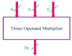
Fig.5. Three-Operand Multiplier Cell
In this architecture a three n-bit inputs are fed in to the circuit simultaneously, as shown in Fig. 5. Then the 3-step process: partial product calculation, partial product reduction, and carry propagation computation is performed inside of the block to get the final result as indicated in the figure. The output of the three-operand multiplier cell is 3n-bit. Here, we like to emphasize that, performing three-operand multiplication on today’s computers need two separate hardware. The latter is referred to as classical multiplier.
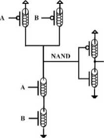
In order to achieve a better performance, the architecture is implemented in transistor level. As it was mentioned, utilizing carbon nanotube field effect transistors could result in a higher performance of a circuit [5]. To implement the proposed three-operand multiplier applying nanotube technology, an AND gate and a full adder cell, presented by Reshadinezhad et al. [23], are used as the main components. The AND gate and the full adder cell designed in CNFET technology, are depicted in Fig. 6.
The full adder presented in [23] consists of 12 transistors and 3 capacitors. Here, the capacitors act as voltage divider. As it is illustrated in Fig. 6(b), the carbon nanotube field effect transistors are utilized to implement Majority NOT, NAND and NOR functions. The output voltage of the capacitor networks of these modules are identical. Transistors with different threshold voltages, evaluate the outputs of corresponding functions. This full adder has a low power consumption and power delay product.
(a)
(b)
Fig.6. (a) AND Gate Using CNFET, (b) Full Adder Cell Based on Carbon Nanotube Technology [23]
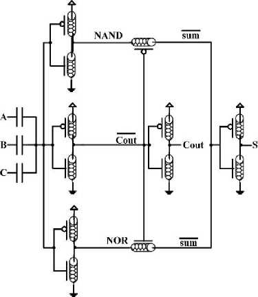
The proposed three-operand multiplier employs AND gates, full adders, compressors and a carry propagating adder in carbon nanotube technology. In order to produce partial products, Fig. 6(a) is used and the nano-AND is resulted, which is shown in Fig. 8. In the reduction stage, either (3:2) or (4:2) CNFET compressors are employed. The nano-full adder with three inputs A, B, and C will result in the outputs of Sum and C out . The (4:2) compressor based on nanotechnology is implemented by applying two back-to-back nano-full adders. Finally, in the last step of multiplication, nano-CPA is implemented through successive nano-full adders that ripple the carry. Implementing each component of nano-multiplier is shown in Fig. 8.
The CNFET three-operand multiplication architecture is illustrated in Fig. 9.In this implementation, the first two operands are multiplied together to generate an 8 bit product result. Then the third operand is multiplied to the product result and goes through all three steps of multiplication and gives the final result.
In order to calculate the total delay of n-bit three-operand multiplier in gate level, (9) is applied.
Т - 2(7 + 2 1О2 л Л + <7,,, 2 1
n х n х n AADD g2 (4:2) CPA (2 n - 3) CPA (3 n - 3)
The CPA and total delay of a three-operand multiplier are calculated through (10).
8 CPA ( n х n х n ) = 28xor + (10 n - 16) 8 add
T n х n х n = 14 P log 2 n 1+ 10 n - 11
Simulation on the implemented design has been performed by HSPICE circuit simulator. For simulating the CNFET circuits, the spice model proposed in [29, 30, 31, 32] has been employed. This standard model has been designed for enhancement-mode unipolar MOSFET-like
CNFETs, in which each transistor may include more than one CNT as its channel. Moreover, this model takes into account a realistic, circuit-compatible CNFET structure and includes practical device nonidealities, parasitics, Shottkey-barrier effects at the contacts, doped sourcedrain extension regions, scattering (nonideal near-ballistic transport), inter-CNT charge screening effects, back-gate (substrate bias) effect and Gate and Source/Drain, resistances and capacitances. The model also comprises a full trans capacitance network for more accurate dynamic and transient performance simulations. The important parameters of the CNFET model, their corresponding values and a brief description, are tabulated in Table 1.
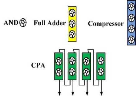
Fig.8. CNFET Components of the Proposed Three-Operand Multiplier
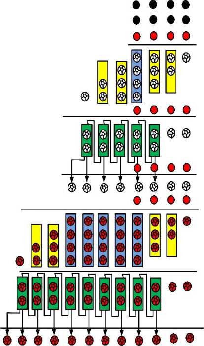
Fig.9. The Proposed Three-Operand Multiplier
Table 1. CNFET Model Parameters
|
Parameters |
Description |
Value |
|
Lch |
Physical channel length |
32 nm |
|
Lgeff |
Mean free path in the intrinsic CNT channel |
100 nm |
|
Lss |
Length of doped CNT source-side extension region |
32 nm |
|
Ldd |
Length of doped CNT drain-side extension region |
32 nm |
|
Kgate |
Dielectric constant of high-k top gate dielectric material |
16 |
|
Tox |
Thickness of high-k top gate dielectric material |
4 nm |
|
Csub |
Coupling capacitance between the channel region and the substrate |
40 pF/m |
|
Efi |
The Fermi level of the doped S/D tube |
6 eV |
To achieve precise estimation of the delay, power and power delay product for comparing the two introduced architectures, circuits have been simulated with Synopsys HSPICE and 32 nm CNFET technology. The simulation results are tabulated in Table 2.
As it is shown in Table 2, the first row corresponds to a 4×4 multiplication. The second row is that of an 8×4 multiplier. The third row is the addition of the first two rows, which corresponds to a classical three-operand multiplier. Finally, the last row is the proposed three-operand multiplier. The simulation results demonstrate the superiority of the proposed design.
The comparison of the classical multiplier and the proposed three-operand multiplier is shown in a bar-chart in Fig. 10. The simulations indicate that putting all the three operands in one architecture and perform the multiplication based on CNFET technology, will reduce delay by 42.39%, power by 65.94% and power delay product by 70.47%.
Table 2. The Simulation Results of Classical Three-Operand Multiplier against Proposed Three-Operand Multiplier
|
Design type |
Main J |
parameters of the circuit |
|
|
Multiplier |
Delay (e-11S) |
Power (e-05W) |
PDP (e-15J) |
|
4×4 Two-operand |
1.9183 |
1.3083 |
0.25096 |
|
8×4 Two-operand |
5.6021 |
8.3956 |
4.7033 |
|
Classical Three-operand |
7.5204 |
9.7039 |
4.9543 |
|
Proposed Three-operand |
4.3318 |
3.3043 |
1.4626 |
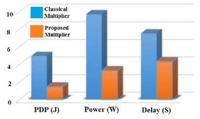
Fig.10. The Comparison of the Classical and Proposed Three-Operand Multiplier Parameters
-
V. Conclusion
The three-operand multiplier design in this article is considered with respect to the effect of the multipliers in arithmetic circuits especially in encryption, filtering and exponential computations. In this paper a novel three-operand multiplier has been proposed. The design is implemented based on carbon nanotube technology.
As it is mentioned, today’s computersutilize two separate hardware, in order to compute three-operand multiplication; while the proposed three-operand multiplier conducts this operation in just one hardware. To implement the proposed multiplier, an AND gate, a full adder cell and a (4:2) compressor based on CNFET are simulated.
All the simulations have been performed in HSPICE using the CNFET model provided by [29]. According to delay, power and power delay product results, it is shown that the proposed CNFET-based three-operand multiplier is superior to that of the classical three-operand multiplier. The presented results expose that the design approach considered is a viable solution for high performance VLSI design CNFET technology.
References Design and Implementation of a Three-operand Multiplier through Carbon Nanotube Technology
- R.Conway, and J.Nelson, "Improved RNS FIR filter architectures," Express Briefs, IEEE Transactions on Circuits and Systems II,vol. 51, no. 1, 2004, pp. 26-28.
- A.Menezes, P. C. Oorschot, andS. A.Vanstone, Handbook of Applied Cryptography, 1996, CRC Press.
- M. R.Reshadinezhad, and F. K.Samani, "A novel low complexity Combinational RNS multiplier using parallel prefix adder," International Journal of Computer Science Issues (IJCSI), vol. 10, 2013, no. 2.
- B.Parhami, Computer Arithmetic: Algorithms and Hardware Designs, Oxford University Press, Inc., 2009.
- G.Cho, Y. B.Kim, F.Lombardi, and M. Choi, "Performance evaluation of CNFET-based logic gates," Instrumentation and Measurement Technology Conference, IEEE, 2009, pp. 909-912.
- S. J.Tans, A. R. Verschueren, and C.Dekker, "Room-temperature transistor based on a single carbon nanotube," Nature, vol. 393, no. 6680, 1998, pp. 49-52.
- Y. B.Kim, Y. B.Kim, and F.Lombardi, "A novel design methodology to optimize the speed and power of the CNTFET circuits," 52nd IEEE International Midwest Symposium on Circuits and Systems, 2009, pp. 1130-1133.
- M. H.Moaiyeri, R. F. Mirzaee, A.Doostaregan, K.Navi, and O. Hashemipour, "A universal method for designing low-power carbon nanotube FET-based multiple-valued logic circuits," IET Computers & Digital Techniques, vol. 7, no. 4, 2013, pp. 167-181.
- J. P.Deschamps, G. J. Bioul, and G. D.Sutter, Synthesis of Arithmetic Circuits: FPGA, ASIC and Embedded Systems, John Wiley & Sons, 2006.
- C. S.Wallace, "A suggestion for a fast multiplier," IEEE Transactions on Electronic Computers, 1964, pp. 14-17.
- J. Y.Kang, and J. L.Gaudiot, "A fast and well-structured multiplier," Euromicro Symposium on Digital System Design, IEEE, 2004, pp. 508-515.
- N.Itoh, Y. Naemura, H. Makino, Y. Nakase, T. Yoshihara, and Y. Horiba, "A 600-MHz 54×54-bit multiplier with rectangular-styled Wallace tree," IEEE Journal of Solid-State Circuits, vol. 36, no. 2, 2001, pp. 249-257.
- N. Azimi, H. Hoseini, A.Shahsavari, "Designing a novel ternary multiplier using CNTFET," International Journal of Modern Education and Computer Science (IJMECS), vol. 6, no. 11, 2014, pp. 45-51.
- S. Mhaske, I. Ghosekar, P. Bhaskar, "Low-complexity wallace multiplier using energy-efficient full adder based on carbon nanotube technology," International Journal of Engineering Research and General Science, vol. 3, no. 2, 2015, pp. 1308-1313.
- W. C.Yeh, and C. W.Jen, "High-speed Booth encoded parallel multiplier design," IEEE Transactions on Computers, vol. 49, no. 7, 2000.
- J. Fadavi Ardekani, "M×N Booth encoded multiplier generator using optimized Wallace trees," IEEE Transactions on Very Large Scale Integration (VLSI) Systems, vol. 1, no. 2, 1993, pp. 120-125.
- G.Jaberipur, and B.Parhami, "Posibits, negabits, and their mixed use in efficient realization of arithmetic algorithms," 15th CSI International Symposium on Computer Architecture and Digital Systems (CADS), IEEE, 2010, pp. 3-9.
- J. N. M.Mori, M.Hirano, S. Tanaka, M.Noda, Y. Toyoshima, and K. Maeguchi, "A 10 ns 54×54 b parallel structured full array multiplier with 0.5 μm CMOS technology," IEEE Journal of Solid-State Circuits, vol. 26, no. 4, 1991, pp. 600-606.
- H.Kobayashi, "A fast multi-operand multiplication scheme," Proceedings of the 7th Symposium on Computer Arithmetic, 1981, pp. 246-250.
- R.McIlhenny, and M. D.Ercegovac, "On the implementation of a three-operand multiplier," ConferenceRecord of the Thirty-First Asilomar, IEEE, vol. 2, 1997, pp. 1168-1172.
- M. R.Reshadinezhad, and K.Navi, "High-speed multiplier design using multi-operand multipliers," International Journal of Computer Science and Network, 2012.
- K.Navi, R. E. S.Rad, M. H.Moaiyeri, and A. Momeni, "A low-voltage and energy-efficient full adder cell based on carbon nanotube technology," Nano-Micro Letters, vol. 2, no. 2, 2010, pp. 114-120.
- M. R.Reshadinezhad, M. H.Moaiyeri, and K.Navi, "An energy-efficient full adder cell using CNFET technology," IEICE transactions on electronics, vol. 95, no. 4, 2012, pp. 744-751.
- M. H.Moaiyeri, R. F.Mirzaee, K.Navi, and A.Momeni, "Design and analysis of a high-performance CNFET-based Full Adder," International Journal of Electronics, vol. 99, no. 1, 2012, pp. 113-130.
- R. Martel, T. Schmidt, HR. Shea, T. Hertel, P. Avouris, "Single-and multi-wall carbon nanotube field-effect transistors," Applied Physics Letters, vol. 73, no. 17, 1998, pp. 2447-2449.
- HT. Soh, CF. Quate, AF. Morpurgo, CM. Marcus, J. Kong, H. Dai, "Integrated nanotube circuits: Controlled growth and ohmic contacting of single-walled carbon nanotubes," Applied Physics Letters, , vol. 75, no. 5,1999, pp. 627-629.
- C. Zhou, J. Kong,H. Dai, "Electrical measurements of individual semiconducting single-walled carbon nanotubes of various diameters," Applied Physics Letters, vol. 76, no. 12,2000, pp. 1597-1599.
- M. H. Moaiyeri, R. F. Mirzaee, K. Navi,O. Hashemipour, "Efficient CNTFET-based ternary full adder cells for nanoelectronics," Nano-Micro Letters, vol. 3, no. 1,2011, pp. 43-50.
- Stanford University, 2014. Stanford CNFET Model. [Online] Available at: https://nano.stanford.edu/stanford-cnfet-model[Accessed 27 9 2014]
- J. Deng,HS. Wong, "A circuit-compatible SPICE model for enhancement mode carbon nanotube field effect transistors," International Conference onSimulation of Semiconductor Processes and Devices, 2006, pp. 166-169.
- J. Deng,HS. Wong,"A compact SPICE model for carbon-nanotube field-effect transistors including nonidealities and its application—Part I: Model of the intrinsic channel region," IEEE Transactions on Electron Devices, vol. 54, no. 12,2007, pp. 3186-3194.
- J. Deng,HS. Wong, "A compact SPICE model for carbon-nanotube field-effect transistors including nonidealities and its application—Part II: Full device model and circuit performance benchmarking," IEEE Transactions onElectron Devices, vol. 54, no. 12, 2007, pp. 3195-3205.
