Design and Implementation of Novel Multiplier using Barrel Shifters

Author: Neeta Pandey, Saurabh Gupta
Journal: International Journal of Image, Graphics and Signal Processing(IJIGSP) @ijigsp
Article in issue: 8 vol.7, 2015.
Free access
The paper presents a design scheme to provide a faster implementation of multiplication of two signed or unsigned numbers. The proposed scheme uses modified booth's algorithm in conjunction with barrel shifters. It provides a uniform architecture which makes upgrading to a bigger multiplier much easier than other schemes. The verification of the proposed scheme is illustrated through implementation of 16x16 multiplier using ISIM simulator of Xilinx Design Suite ISE 14.2. The scheme is also mapped onto hardware using Xilinx Zynq 702 System on Chip. The performance is compared with existing schemes and it is found that the proposed scheme outperform in terms of delay.
Barrel shifter, modified Booths algorithm, multiplier design
Short address: https://sciup.org/15013896
IDR: 15013896
Text of the scientific article Design and Implementation of Novel Multiplier using Barrel Shifters
Published Online July 2015 in MECS DOI: 10.5815/ijigsp.2015.08.03
Due to the recent advancements in the field of multimedia and communication technologies, real-time processing requirement of image, graphics and signals has become more and more important. Multiplication is one of the most important arithmetic operations. It is used in almost all systems that perform any sort of image processing, analog or digital speech processing or any multimedia related operation. Some of the common examples include convolution, inner product, Discrete Wavelet Transform (DWT), Fast Fourier Transform (FFT) etc. For efficient and fast operation of such systems, high speed multiplier is a must requirement. Its importance can be seen from the fact that most DSPs and high end processing systems use a separate multiplier unit for fast multiplication.
Barrel shifter is instrumental for expeditious processing of data in both general purpose and embedded digital signal processors. It is primarily combinational circuit made up of multiplexers wherein the signal passes through constant number of logic gates, thereby making the delay almost fixed, which is independent of the shift value or shifter size. The design of a barrel shifter is hierarchical in a sense that the layers of the multiplexers are linked with each other such that the output of one multiplexer is connected to the input of the next multiplexer and the connection depends upon the required shift distance. An N bit barrel shifter may be constructed by placing N 2:1 multiplexers in log2N layers. Thus an 8
bit barrel shifter requires three layers each having eight 2:1 MUX as shown in the Fig. 1. Here inp(j), out(j) and shift(k) corresponds to jth bit of input, jth bit of output and kth bit of select input; and values of j and k assume values in the range of 0-7 and 0 – 2 respectively. The selection lines of the MUX in ith (i = 1,2,3) layer are connected to (i-1)th bit of shift input. The layer provides shift by 2i-1 bit positions if corresponding (i-1)th bit is high. For shift input of “100” the first two layers pass inputs without any shift and third layer shifts input by four bit positions. It be noted that 8 bit barrel shifter can shift a word by 0-7 bit positions (0 being the trivial case) by combining shifts in all the three layers. An n bit position shift operation in barrel shifter can be performed in single cycle in contrast to ‘n’cycles in a shift register due to its combinational logic structure. These type of shifters are already used in the floating point add and subtract operations which require proper alignment of the mantissa of the operands [1, 2]. This paper investigates the possibility of using barrel shifters in multiplication where shifting is required rather frequently.
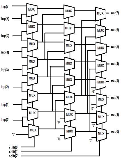
Fig. 1. Barrel Shifter design [1]
The paper is organized as follows: Section 2 briefly describes multiplier architectures followed by proposed design in Section 3. The hardware implementation on Zynq 702 SoC is explained in section 4. Section 5 describes the results as obtained after the implementation and Section 6 constitutes the conclusion and future prospective of the proposed algorithm.
-
II. Related Work
Numerous designs of multipliers have been proposed in [3-8] and references cited therein. The designs have a tradeoff between the number of parallel units used for implementation and the maximum clock period with which the circuit can operate. The conventional shift-add algorithm is the most basic multiplier that makes use of repetitive shifting and accumulation of multiplicand in accordance with the multiplier. It multiplies two ‘n’ bit numbers in 'n' clock cycles and thus becomes very lengthy as the number of multiplier bits increase. Although the method requires basic arithmetic operations but demands multiple clock cycles to execute. To overcome this, a combinational design consisting of logic gates and adders is presented and named as array multiplier. In this, the partial products are generated by multiplying each multiplier bit one by one with the multiplicand. The partial products terms are then shifted according to their bit order as defined by shift and add algorithm and then are added up to give final output. This type of multiplier is well suited when the operand size is small, but the design complexity increases manifolds for larger size operands. Other multiplication methods are: Braun multiplier, Baugh-Wooley multiplier, Booth multiplier, Wallace tree multiplier. The Braun multiplier has highly regular structure and is useful in applications where area is of prime concern and speed can be traded off. It uses carry save adders foor adding the intermediate partial product terms and then produces the final result in binary form using ripple carry adder. It can deal with only unsigned numbers which becomes motivation for the Baugh-Wooley multiplier. This multiplier takes advantage of the fact that direct multiplication using 2’s complement method can produce the final result directly without requiring complement stages in between, thereby speeding up the process. Further, as the multiplication is done in 2’s complement form, signed numbers are automatically taken into account. Both Braun and Baugh-Wooley multipliers are efficient and have uniform structure but are suitable for handling operand sizes less than 16 bits. Booth multiplier provided a significant advancement in this field. The algorithm takes into account that in all other multiplication algorithms one partial product term is generated for each multiplier bit. This algorithm reduces the number of partial products by representing the original multiplier in a higher radix format. As a significant time is used up in the addition process, the reduction in intermediate terms saves a lot of time and hardware cost. The modifications on this method show improvements in overall speed and implementation area. The Wallace tree multiplier is popular in high speed applications and is characterized by complex and irregular routing. It incorporates a special tree structure, wherein the product terms are first grouped together and then added. Because of grouping, less number of additions are required at each stage. Thus the addition complexity is reduced down from O(n) to O(log n). Many compression techniques have been proposed for Wallace tree which further reduces the effective number of additions at each layer of the multiplication process and thus providing better timing results. But due to irregular structure and complex routing, power consumption becomes an important problem for this. Wallace tree is commonly used in conjunction with the booth encoder thereby having the advantage of both the methods and has timing results superior to that of others.
In this work, we have proposed a multiplier design that uses barrel shifters in conjunction with modified booth’s algorithm to develop a high speed multiplier circuit. The proposed design can perform both signed and unsigned multiplication. It is then implemented over hardware using Zynq 702 SoC.
-
III. Proposed Design
This section describes a novel multiplier design based on barrel shifters which takes into account the single clock shifting capabilities of barrel shifters which are utilized to produce the partial products in a parallel fashion. Here the partial products are the shifted version of the multiplicand (Y) accounted on basis of the multiplier (X) bits. The design first uses barrel shifters to produce partial products which are then added up using adder tree. The utility of the proposed multiplier is further enhanced as it can multiply both signed and unsigned numbers by incorporating sign extension of the partial product terms. In addition to the proposed parallel architecture, the design also integrates Booth's encoder which uses modified Booth's algorithm. Due to this the number of partial products reduces from 'n' to 'n/2', 'n' being the number of bits in multiplier which in effect reduces the number of additive layers by one thereby improving the delay by great extent. The following section describes the proposed design step by step.
Table 1. Radix-4 booth encoding
|
Block |
Partial product (operation) |
|
000 |
0 |
|
001 |
+1*multiplicand |
|
010 |
+1*multiplicand |
|
011 |
+2*multiplicand |
|
100 |
-2*multiplicand |
|
101 |
-1*multiplicand |
|
110 |
-1*multiplicand |
|
111 |
0 |
A. Booth’s Encoder
The modified booth's algorithm [6] i.e. radix-4 booth's encoding is briefly explained in this section. Here the multiplier bits (n) are considered as blocks of 3 bit each where two consecutive blocks have one bit in common as shown (1).
- To keep signed multiplication into consideration too, the true or the complemented form is extended with the sign bit to '2n' bits i.e. double the number of bits in the multiplicand.
D3
D.
X = £ D i 4 i i = 0
X X X X X X X X|0
After the barrel shifters are fed with legal inputs then the data word is shifted by the required amount as set by the index of the pair that was formed by the booth encoder. In general, each barrel shifter has shift equivalent of 2(k-1) bits where ‘k’ signifies the ‘kth’ encoded multiplier bit group from the booth’s encoder.
d2
Do
The grouping in multiplier starts from least significant bit (LSB) with a zero bit appended to it. The overlap between the block signifies what happened in last block as the MSB of each block acts like its sign bit. As an example if a 16 bit multiplier is “0010110010010011”, then the pairs are as formed as in (2).
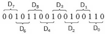
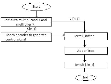
Fig. 2. Data Flow in proposed design
The multiplicand is either evaluated to zero, multiplied by ±1 or ±2 according to the 3 bit pairs. The exact operation is summarized in Table 1.The MSB of each pair gives the sign with which the corresponding partial product is to be sign extended. As the modified booth’s algorithm reduces the number of partial product terms to half as compared to the conventional multiplier, the former requires lesser number of total resources and also has significant speed improvement.
-
B. Proposed Scheme
The data flow in the proposed design can be described by the flowchart of Fig. 2. The proposed design uses three steps- booth encoding, partial product generation by barrel shifters followed by the addition. Here the x [n-1] and y [n-1] signifies the multiplier and multiplicand respectively, each ‘n’ bit wide. The steps for partial product generation are:
-
- Firstly the multiplier is fed into the booth encoder circuit which in turn generates a control signal to control the input to the barrel shifter.
-
- According to the control generated, the barrel shifters are fed in with either multiplicand in its true form or in 2's complement form.
-
- The barrel shifters are placed so as to provide a fixed number of bit shifting according to the index they are operated upon.
The barrel shifters output reduced partial terms which are to be added to form the final result. For unsigned numbers 'n' bit adders are sufficient for the purpose as the partial product terms are '2n' bits in size but 'n' bits out of these are just zeros, so effectively we need to add only 'n' bit numbers for each partial product term. For signed numbers though we have to use '2n' bit adders, as the partial product terms contain the extended sign bits which have to be taken into account while performing the addition. For efficient adding an adder tree is prepared depending on the number of partial products to be added, as this reduces the number of levels in which addition takes place. For this purpose different types of adders may be incorporated into the design like Ripple Carry Adders, carry skip adders, carry select adders, carry increment adders, carry look ahead adder, tree adders [37]. Parallel-prefix adder tree structures such as Kogge-Stone [9], Sklansky [10], Brent-Kung [11], Han-Carlson [12], and Kogge-Stone using Ling adders [13] etc. have one or other advantage over other. The performance of the ripple carry adder is linearly proportional to the number of bits whereas carry bypass, carry select and carry look ahead show square root and logarithm dependence on number of bits. Though the carry look ahead adder provides a significant improvement in delay but becomes inefficient for wide adders as the total delay is dominated by the delay in passing the carry through
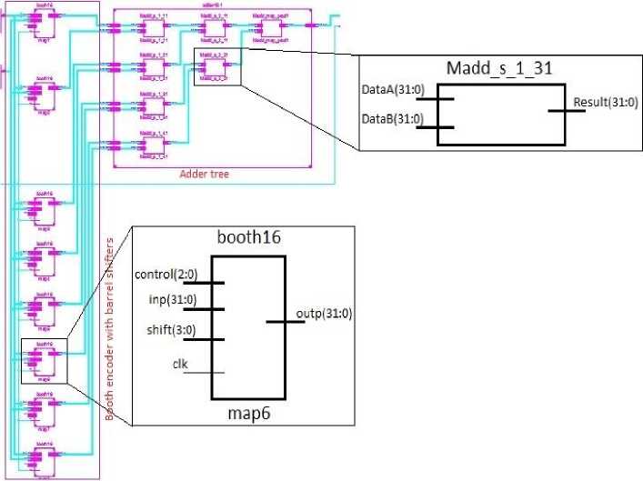
Fig. 3. RTL schematic view of 16x16 multiplier
look ahead stages which can be handled by arranging the look ahead stages in a multilevel tree. Such adders are known as tree adders and some of the examples are Kogge-Stone [8], Sklansky [9], Brent-Kung [10], Han-Carlson [11], and Kogge-Stone using Ling adders [12]. The choice of a particular adder depends on the number of stages of logic, the number of logic gates, maximum fan out on each gate and amount of wiring between the stages. After the addition, the output is stored in a ‘2n’ bit wide output register. The focus in the present work is to establish the concept of barrel shifter in multiplier implementation, therefore default adder available in FPGA in hardware implementation.
-
IV. Harware Implementation
The proposed multiplication scheme is verified by simulating a 16x16 multiplier in Xilinx Design Suite ISE 14.2. The simulations have been performed using Integrated Software Environment (ISE) included in the Design suite. The scheme is mapped onto hardware using The RTL schematic view of the design showing the various blocks for a 16x16 multiplier is as shown in the Fig. 3.
From left to right the schematic may be viewed in 3 blocks namely the booth encoder, barrel shifter and adder. The 16 bit wide multiplier and multiplicand inputs are stored in registers, an input clock signal to drive the registers and then the final output fed to a 32 bit register. The number of parallel units in the structure depends upon the number of bits which are to be multiplied. Here for 16x16 multiplication, the booth encoder generates 'n/2' i.e. 8 partial product terms thus in total we require 8 barrel shifters which shift the product terms as required in the multiplication algorithm. From the enlarged section comprising booth encoder with barrel shifter has namely 4 input ports control(2:0), inp(31:0), shift(3:0) and clk which correspond to 3 bits of multiplier which will be encoded by booth encoder, the multiplicand, 4 bits to specify required shift value and the clock signal. The output is shifted 32 bit version of the multiplicand. Further then the shifted vector go through an adder tree, each adder having two 32 bit vectors as inputs and giving back an 32 bit output.
The barrel shifters facilitate the shifting operation unlike conventional sequential shifters where the data is shifted one bit position per cycle. Thus the partial product generation becomes faster and results in improved speed performance of the multiplication process. The adder circuit is implemented in the form of a binary tree where each adder is 32 bit wide as each of the partial product terms are of 32 bits due to the extension of the sign bit which has to be taken into consideration for the multiplication of signed numbers. The adder circuit can be implemented using various techniques available. The default adder of FPGA is used to test the proposed method.
The graphical design view, obtained in the Xilinx Platform Studio (XPS) is shown in the Fig. 4 for the target FPGA (Zynq 702 Soc) device where the design is finally ported.
Xilinx Zynq 702 System on Chip is a general purpose board having advantage of parallel units (configurable logic blocks (CLB's)) as well as sequential unit (ARM Cortex A9 Duel core processor). Embedded Design Kit (EDK) is used to model the multiplier in VHDL language.
Further, to communicate with the on-chip processor Software development kit (SDK) is used which serves as a medium to give input to the multiplier and collect the final output. Finally the design is mapped on the FPGA using the bit stream generated in PlanAhead tool.
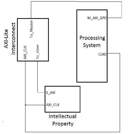
Fig. 4. Block diagram of implemented design over Zc702 evaluation board
The logic of the hardware is implemented as an intellectual property (IP) in the programmable logic (PL) section of the device. The hardware block is driven by the processing system (PS) through an AXI4-Lite bus based on AMBA protocol which is light weight, single transaction memory mapped interface running at 50MHz. The board provides a serial interface (USB) for feeding the data to the hardware. The transaction of operands between the processor and IP is byte oriented i.e. the data is transferred one byte per clock cycle. As shown in figure the processing system is connected to our IP through a AXI interconnect which acts as a interface between the processor running at 800MHz and IP running at 50MHz.The inputs and output are provided by memory read and write operations respectively by specifying the 32 bit address in memory where the hardware block is physically present. The IP is customized to have 3 registers in its wrapper module which by default are 32 bit in size. The input operands are provided in the lower half of two input registers and the final result is collected in a 32 bit output register. The final output can be viewed in the console as provided by Xilinx in Software development kit (SDK).
Further for the purpose of comparison a 4x4 multiplier prototype is also designed and compared with other schemes. The synthesized timing values specifying the delay and maximum operational frequency is shown in the next section.
-
V. Simulation Results
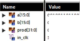
The ISIM simulation results for the 4x4 and the 16x16 multiplier are shown respectively in Figs. 5 and 6 respectively which verify the functionality of the proposed approach. For both cases, the result is available in the output register at the rising edge of input clock after one clock period of application of input operands.
|
Name |
Value |
|
► Ч аВД |
1011 |
|
► 4 bM |
оно |
|
► ^ prod[7:O] |
11100010 |
|
1^ in.dk |
1 |
|
999,900 ps । । । । 1 । । । । |
l,000,00( Illi |
ps Illi |
1,000,10( iiii |
ps IIII |
1,000,200 ps । । । । 1 । । । । |
|
|
uuuu ) |
1011 |
|||||
|
uuuu ) |
r~ |
0110 |
||||
|
; ini |
0010 |
|||||
|
— |
— |
— |
— |
|||
Fig. 5. Simulation results of 4x4 multiplier
IlUUUUUUUUUUU...
IlUUUUUUUUUUU...
999,900 ps __l__L_1__l_J___I___L
1,000,000 ps
___I___I___I—I___ L_l___ I___L
1,000,100 ps ____I I I—I I I L
1,000,200 ps
_1__I__"il l__I__L
Fig. 6. Simulation results of 16x16 multiplier
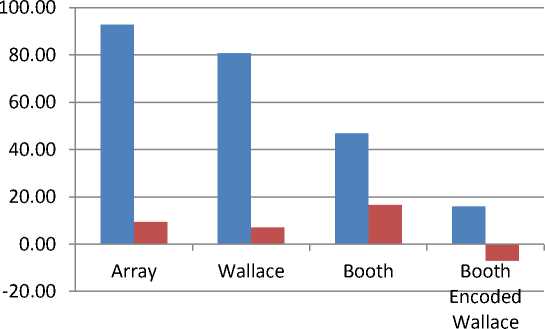
A comparison of the proposed multiplier is carried out in reference to Shift Add multiplier, Array, Wallace tree, Booth, Booth encoded Wallace tree and the results are summarized in Table 2. The proposed design has the lowest delay time when compared to that of other’s and hence can operate at a clock frequency as high as 788 MHz. Further, a comparison listing the resource utilization is provided which shows the efficient nature of proposed design. Fig 7 gives a graphical representation of the same from which it is clear that the proposed design is much better that the others in both delay and area except for booth encoded Wallace where the area requirements are more by 7% but gives around 16% improvement in timing parameter.
Table 2 Comparison of proposed design’s results
|
Type of Multiplier |
Delay (ns) |
Maximum operational frequency (MHz) |
No. of Slice LUT’s utilized |
|
Shift Add multiplier |
3.930 |
254.453 |
63 |
|
Array |
2.448 |
408.497 |
46 |
|
Wallace tree |
2.295 |
435.730 |
47 |
|
Booth |
1.864 |
536.481 |
49 |
|
Booth encoded Wallace tree |
1.471 |
679.809 |
39 |
|
Proposed design |
1.269 |
788.022 |
42 |
■ Delay
■ Area
Fig. 7. Comparison of proposed design with other’s for delay and area
-
VI. Conclusion
A multiplier design based on barrel shifter is presented in this paper. The proposed scheme makes use of modified booth's algorithm in conjunction with barrel shifters for improving the delay. The functionality of the design is verified through simulations and performance is compared with existing multipliers. The proposed design shows 16% improvement in delay therefore it can operate at much higher operating speed. Further the proposed multiplier accounts for signed multiplication as well without adding any more complexity. Thus the simplicity and hierarchical design makes it very easy for designing and debugging. Due to these advantages, the multiplier can be used in high speed processing devices such as DSP’s etc. The work can further be extended for optimization of proposed multiplier in terms of area and power.
References Design and Implementation of Novel Multiplier using Barrel Shifters
- J. H. Cline, "Barrel shifter using bit reversers and having automatic normalization", US 4782457 A, 1988.
- M. J. S. Smith, Application Specific Integrated circuits, Pearson, 2006.
- M. Ercegovac, and T. Lang, Digital Arithmetic, San Francisco, Morgan Kaufmann, 2004.
- B. Pahrami, Computer Aithmatic and Hardware Design, New York, Oxford University Press, 2000.
- N. H. E. Weste, D. Harris, and A. Banerjee, CMOS VLSI Design: A Circuit and System perspective, Pearson, 2006.
- M. Rabaey, A. Chandrakasan, and B. Nikolic, Digital Integrated Circuits A Design Perspective, PHI, 2003.
- K. S. Yeo, and K. Roy, Low Voltage Low Power VLSI Subsystems, Tata Mc-Graw Hill, 2009.
- V. Kunchigik, L. Kulkarni, and S. Kulkarni, "Pipelined Vedic-Array Multiplier Architecture", International Journal of Image, Graphics and Signal Processing (IJIGSP)", vol. 6, No. 6, pp. 58-64, 2014
- P. M. Kogge, and H. S. Stone, "A parallel algorithm for the efficient solution of a general class of recurrence equations", IEEE Transactions on Computers, vol. C-22, pp. 786–793, 1973.
- J. Sklansky, "Conditional-sum addition logic", IRE Transactions on Electronic Computers, vol. 9, pp. 226–231, 1960.
- R. P. Brent, and H. T. Kung, "A Regular Layout for Parallel Adders", IEEE Transactions on Computers, vol. C-31, (1982), 260–264,.
- T. Han, and D. Carlson, "Fast area-efficient VLSI adders", in Proceedings of IEEE Symposium on Computer Arithmetic, pp. 49–56, 1987.
- H. Ling, "High-speed binary adder", IBM Journal of Research and Development, vol. 25, pp. 156–166, 1981.
