Design of an arbiter for two systems accessing a single DDR3 memory on a reconfigurable platform

Author: Arun S. Tigadi, Hansraj Guhilot
Journal: International Journal of Information Engineering and Electronic Business @ijieeb
Article in issue: 6 vol.10, 2018.
Free access
The computer memory has been revolutionized in the last 25-30 years, in terms of both capacity and speed of execution. Along with this, even the logic controlling the memory has also become more and more complex and difficult to interface. Usually, memory subsystems will be designed to interact with a single system. Whenever we consider a two system is sharing a common memory, there comes the need for an Arbiter. The major difference between a memory arbiter and a processor scheduler is that the memory arbiter works at a much finer level of granularity. The time taken for the task execution may range from micro to milliseconds, while a RAM controller needs to serve the request in a few nanoseconds. Because of this reason the resource arbiters are usually designed and implemented in hardware rather than in software.
Arbiter, memory controller, FPGA(Field programmable gate Array), SDRAM (Synchronous DRAM)
Short address: https://sciup.org/15016152
IDR: 15016152 | DOI: 10.5815/ijieeb.2018.06.02
Text of the scientific article Design of an arbiter for two systems accessing a single DDR3 memory on a reconfigurable platform
Published Online November 2018 in MECS DOI: 10.5815/ijieeb.2018.06.02
The computer memory has been revolutionized in the last 25-30 years, in terms of both capacity and speed of execution. Along with this, even the logic controlling the memory has also become more and more complex and difficult to interface. Normally, memory subsystems are designed to interact with a single system but when two or more systems need to communicate; there rises the need to share a common memory which will create conflicts while accessing this shared memory. So to resolve these conflicts arbiters are needed.
The major difference between a memory arbiter and a processor scheduler is that the memory arbiter works at a much finer level of granularity. The time taken for the task execution may range from micro to milliseconds, while a RAM controller needs to serve the request in a few nanoseconds. Because of this reason the resource arbiters are usually designed and implemented in hardware rather than in software. The arbiters are the part of scheduler design in which request and grant signals are designed keeping the priority issue in mind so that whenever it is required the priority state can be updated. In most of the systems, it is required to access a common resource by many requestors. The common resource considered can be a networking switch, a special state machine, shared memory, or a computational element.
Attention should be paid to various factors for the design of an arbiter. The size and speed of the arbiter will decide the design of even the interface design between the requester and the arbiter. As the technology is improving, we are moving in the era of multi-billion transistor SoCs containing multiple processing elements (PEs). The buses and the memory will act as the communication between the PEs and the SoC. The fast and powerful arbiter requirement will increase as the bus master increase on a single chip. An arbiter is a component which will be deciding how the resource is being shared among many requests. Many standard memory modules are designed for using them with the single system.
The arbiter has to follow certain rules to choose which system gets through to the memory controller. Usually, the arbiter needs to follow certain rules to pass the communication between the blocks. Arbiters find multiple applications, but in this case, it will be implemented on a FPGA between some systems and a single memory module. To fairly share the resource, the arbiter needs to take appropriate consideration. The synthesis results will be affected by the coding style. The three fundamental components on which arbiter works are: Request, grant and accept. The DDR3 is one of the newest and the fastest volatile memory available in the market now. It is one of the different types of random access memory available which will temporarily hold the data for the sake of system to have quick access.
-
II. Related Work
In the year 2001 Author Matt Weber published the paper " Arbiters: Design Ideas and Coding Styles." This paper contains a few outline thoughts for adequately interfacing with a referee and research coding styles for some regular discretion plans. For different applications, the framework fashioner must plan a controller to give legitimate summons to SDRAM introduction, read/compose gets to, and memory invigorate.
In the paper titled "Hard IP Core of Memory Arbiter" published in the year 2013 by the authors Kedar Trivedi, Nandish Thaker at the “International Journal of Advanced Research in Computer and Communication Engineering “They explained the plan of 4X4 memory judge and it’s outcomes.
-
III. Memory Interface Generator
The Xilinx Memory Interface Generator is located within the CORE generator of XPS [3]. The memory interface, or memory controller, is composed of many modules which allow both communication with and testing of the memory. The memory controller handles communicating with the high-speed interface of the DDR3 so that we don’t have to. Therefore, our user design only needs to account for interfacing with the memory controller.
-
A. Memory Controller Hierarchy
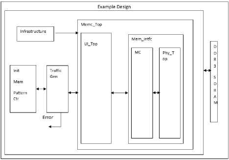
Fig.1. Design Block Diagram
Position, The memory controller, is contained within the wrapper, example_top, shown in Figure 1 as example design. Within example_top, there are four overarching modules: memc_ui_top, infrastructure, m_traffic_gen, and init_mem0 (init_mem_PatterCtr).
memc_top: this defines the top level module of the memory controller. Its function is to convert the given address into respective rows , columns and banks for actual to and from data transfer towards the memory.
Infra: All the modules will get the clock through this.
m_traffic_generator: This module generates the variety of commands and data patterns for the purpose of memory testing .The expected and the actual read data are compared to find the faults.
init_mem0: This module seeds m_traffic_gen’s fifos with commands, addresses, and data.
-
IV. Interfacing with Mig
Since it was my assigned task to create my own arbiter, we eliminated the option of using the AXI4 interface. Reordering of the data from the memory is required by the native interface, which intern makes the arbitration between two systems much more complicated one.
We can reorder the commands by the user interface and create a simpler design; the user interface is created for the interaction with the memory.
Figure 2 describes the user design (arbiter) and memory (DDR3 SDRAM).The user interface provides the immediate way to interact with the memory. As per the design we need to consider only the signals between the UI and the user design. Figure 2 the arbiter design needs to account for.
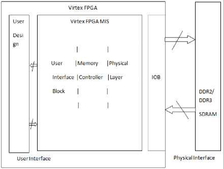
Fig.2. User Interface between User Design and Memory
-
• Bursts
We chose to implement DDR3 utilizing the maximum allowed burst length of 8. This ensures maximum data throughput. The actual memory has a 64-bit interface. A burst of eight (BL8) requires eight 64-bit packets of data to be sent to memory in a row. Since the Xilinx user interface is 256 bits wide, the arbiter sends to the memory controller user interface about 256-bit packets. There will be two 256-bit packets, or 512 bits in total, so it constitutes around burst of 8. So for every 512 bits sent there will be only one address and command.
-
• Command and Address
A address will be sent to a memory for every data packet of 512 bits.
To send an address app_cmd, app_addr, and app_en must be set for one clock cycle. Only when app_en is asserted, are the values on app_cmd and app_addr sent. If the app_rdy signal is de-asserted, the values will not be sent to memory and must be held until app_rdy is high again. Refer to Figure 3 which shows app_rdy low avoidance.
app_cmd: Indicates current request (read/write).
app_addr: Address for current request.
app_en: Asserted to send a command and a address (101).
app_rdy: It indicates whether the UI is ready for accepting the commands (75).
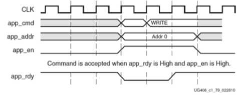
Fig.3. Sending a Command and Address to the Memory Controller
Arbitration for Two systems to one DDR3 memory
In our case the most important specification is to allow two unique systems to communicate with a single memory. The Xilinx memory controller core allows for a single system interaction with the DDR3 memory. The Xilinx memory core acts as the interface between the arbiter design and the DDR3 memory.
I/O synchronising for different clocked systems
Multiple systems working at different frequencies will be connected to the memory controller and with one another with the help of arbiter. FIFO (i.e. first in, first out) blocks are the solution to synchronize the data flow between the memory controller and the system.
When the tem sends the read and write commands in chain of burst length 8 then the controller operates at its peak performance. Two clock cycles are required to complete each of the BL8 burst and it consists of two 256-bit data packets. Since the max operating frequency at 200MHz, the data flow rate may reach up to the speed of around 51.2Gb/s.
Max Speed = —^Bits * Fmax(1)
„ л г, л> 200million cycles
Fmax = 200M hz = (2)
seconds
, 256Ы ts 200m 1111 on cycl es _ 512 GB/
Max speed= -yc^- * seconds - ■ /second
This speed is confirmed by the ML605 Hardware User Guide which states that the evaluation board’s DDR3 SDRAM has been tested to 800MT/s. As we split the memory controller between two systems , so that each system would be able to achieve a half the data flow rate (i.e. 25.6 Gb/s). Here the BW of one working system will affected by both the speed of the second system and the speed of the memory controller.
-
V. Design Topology
The block diagram in Figure 5 shows the design topology of the arbiter configured for two independent systems sharing one memory. It displays how the two independent systems are connected to the DDR3 memory, with the arbiter and the shared memory controller. The infrastructure module, which is not shown in the block diagram, generates the clock for the DDR3 and memory controller module.
-
❖ example_top wrapper
It will act as a wrapper design .The ports used will be connected to the physical pins of the FPGA and to the memory, the two systems.
-
❖ memory_controller
This module simplifies the communication to the memory, because it takes care of the refresh cycle and enables to use BL8 interface. In case of BL8 every address is 512-bit data packets.
-
❖ arbiter_block
This module is used to buffer the read and write commands between the system and memory controller. The FIFO read and write controlling will happen with the state-machine in the arbiter block.
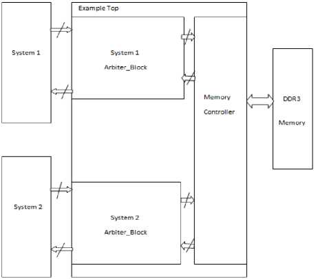
Fig.4. Two arbiter_blocks set-up to connect the DDR3 memory to two different systems
Determining the Arbiter’s Performance
The arbiter’s maximum performance is ultimately capped by the frequency of the memory controller. Typically this frequency runs between 100MHz and 200Mhz, and the memory controller is able to send and receive 256 bits every clock cycle. Since the systems are allowed to send the 64 bits of data at every clock cycle, then the highest efficiency will be obtained at the four times the clock speed of memory controller. If the system is operating at a lower frequency then it will be the under utilization of the arbiter. If the system is running at the four times the frequency of the memory controller then arbiter will become overwhelmed and dynamically it will try cutting down the system’s effective BW. While the memory controller clock sets the cap on the arbiter’s performance, the frequency of the system also acts as the limiting factor on each others effective BW. A mathematical model can be developed to estimate the performance of the arbiter. The effective frequency of a system is derived by the ratio of how many cycles the arbiter per second gives a system control.
Feffective = = -^^2- (4)
П1+П2 n1*/2+n2*/1
/1+/2 ' ’ n1 and n2 represent number of cycles system 1 and system 2 work together every time they are given with the permission to send the commands. f1 and f2 are the frequencies of the two systems. In the above derivation the total time for an arbiter to complete a full cycle in its state machine is expressed as n1/f1+n2/f2 . The effective frequency of one of those systems may be evaluated by taking the ratio of the number of cycles that system has control for by the total time. The data flow may then be evaluated by factoring the effective frequency by 64, which is the number of bits that are sent and received by each clock cycle(data bus width). The model for the data rate would than equal:
BW effective =
64*n1*/1*/2 n.1*f2+n.2*f1
By default, the arbiter is balanced so that both systems are given the same number of the clock cycle for sending their commands. This simplifies the model further into:
BW effective =
64*/1*/2 F2+f1
The thing which can be noted from the above model is that both the systems will be in harmony to have the same BW even under different operating frequencies. This is can be considered as one of the most useful characteristics as it allows for the two systems, irrespective of their individual speeds to have the same speed to communicate with the memory.
-
VI. Emulating Systems
The behavior of the expected system will be modeled to validate the arbiter. To mimic the interaction between the system and the arbiter a stimulus model will be created. These virtual systems will be triggered to send the set of reads and writes by asserting a signal. The model used for stimulus will follow the arbiter’s protocol. It will be having trigger to enable both read and write chains of 32 data packets with addresses 0-31.Usually the write chain will be initiated first then the read chain. Because the read chains read from the same address which the write chain had previously written to, the resulting read-back data is expected to match the write data.
-
A. Switching branches
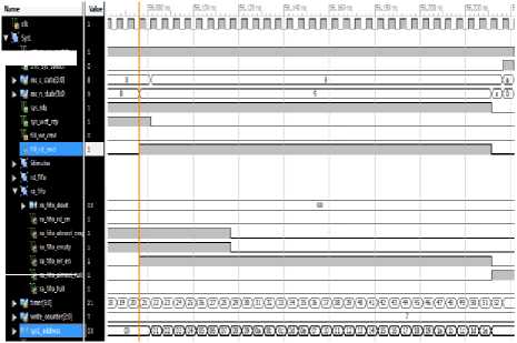
Figure 5 shows one of the systems switching into the system-to-arbiter branch where the system, sys1, can now send either read or write commands to the arbiter. The sys1 will enter into S8 state of the state diagram only when the sys1 enters the system-to-arbiter branch.By asserting the sys_rdy and sys_wdf_rdy signals it notifies the sys1 that it is ready to access new read and write commands. Along with this, the register will keep track of clock cycles that the system has utilized. Once the Sys1 finishes it communication with the arbiter then the Sys2 which is in state 10, which is waiting for the Sys1 to finish its interaction will simply continue with its other tasks.
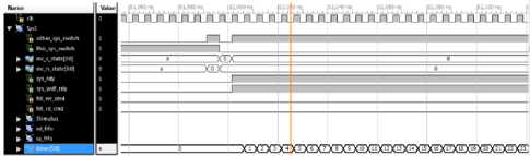
Fig.5. Switching Branches
-
B. System-to-Arbiter Write
As shown in below figure 6 Sys1 starts sending write commands.At the start of each new write commands, Fill_wr_cmd signal will be asserted summing it to four times assertion of Fill_wr_cmd signal. By having a glance at the sys1_addredd waveform, we can notice that four writes right from address zero to address three. Each data transfer is of 64 bits, where each of the 0th bit in each of the 64 bits will make an 8-bit value corresponding to the address[15]. The binary value 00 at address zero, is apparent because of sys_wdf_data[0] and binary 11 at address three. Once the timer register reaches a value of 63, it will halt the sys1 , now the sys2 may enter the arbiter block.
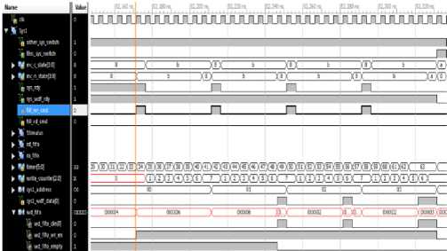
Fig.6 System-to-Arbiter Write
-
C. Arbiter executing buffered Writes.
The arbiter sends write commands to the memory controller between state 1 and state 2. During state 1 the arbiter sends the first half of each 512-bit data packet, and during state 2 it sends the second half of the packet. The address is sent during state 2, with the second part of the data packet.
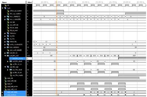
Fig.7. Arbiter-to-System Write
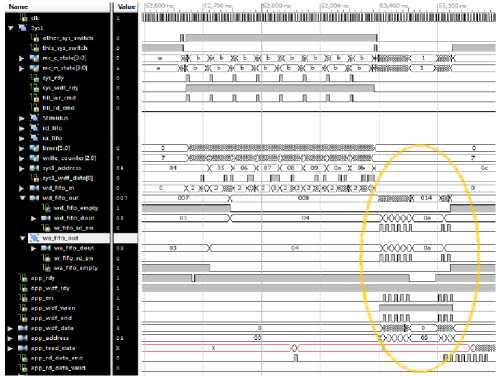
Fig.8. Arbiter successfuly avoiding app_rdy low
For example in Figure 8 above, the waveforms demonstrate additional coverage of the case where the memory controller might de-assert its app_rdy signal in the middle of the arbiter attempting to write. It is important for the arbiter to be able to avoid this hazard, and as can be seen, by the waveforms it does so by extending its state 1 until app_rdy is high again. It is really important to assure that the arbiter design avoids these kinds of circumstances early in the design process so as to minimize the amount of bugs we may get at the end.
-
D. System-to-Arbiter Read commands
After the write commands are sent to addresses 0-31, the stimulus module is then also triggered to send read commands to the same addresses. Figure 9 above displays the waveforms that are generated when the system attempts to read. After its first read command when the timer is at 21, the arbiter’s state changes from state 8 to state 9. At state 9 the system continues to send read commands, as it is permitted to do so because of the asserted sys_rdy signal. However, sys_wdf_rdy goes down in state 9, which means that the system is not allowed to send any write commands. During this branch, the system sends read commands to addresses 0 to 18(1e), which are all buffered in the read address fifo, ra_fifo. The arbiter ends the branch when the ra_fifo fills up as can be observed at timer 52 where the ra_fifo_full signal is asserted. In its next branch, the arbiter will empty out the ra_fifo and send the buffered read commands through the memory controller.
# 1а."П0.аГ0Я_П1
Fig.9. System-to-Arbiter read requests
Lg otter, yjwtto lb thii sk Midi
E. Arbiter-to-System Read execute
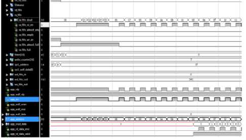
Fig.10. Arbiter-to-Memory read execution
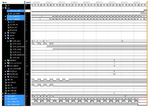
Fig.11. Arbiter-to-Memory read-back
Figure 10 shows the behavior of the arbiter block during its arbiter-to-memory branch where it empties out its ra_address FIFO and sends read commands to the memory controller. All the read commands are combined together and are transferred at the rate allowed by the memory controller. For every clock cycle a read request is allowed by the memory controller ,but after this the memory controller starts to periodically de-assert its app_rdy signal, and as a result arbiter only sends new read commands every two clock cycles.
F. System-to-Arbiter Read-back
After entering the System-to-arbiter branch the arbiter block, it will see that it has data being buffered in its rd_fifo, so it enters state 7. After elapse of 8 clock cycles the rd_fifo will release the data packets of size 512 bits during this state. A series of eight 64 bit packets will be formed out of 512-bit data packets and are sent back to the system.The 0th bit of these 64-bit data packets are identified by the Sys_read_data[0] and the eight-bit representation of 512-bit data packets are shown by the readback_data_reg as they are being released from the rd_fifo. The 64th bit of 512-bit data packet is formed by these bits. The read-back and the write data of the system match with each other validating the arbiter design.[15]
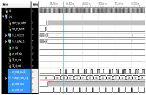
Fig.12. System-to-Arbiter Read-back
-
VII. Conclusion
Designing the arbiter was challenging because the design specifications constantly changed as we became more familiar with the technology, and tools that were available to us. Specifications were affected when we found better ways to do thing, when we noticed flaws in the design, or when the design simply wasn’t working. Overall, learning how to communicate with the memory controller and designing arbiter fostered knowledge about memory, debugging, performance, and many logic design concepts.
References Design of an arbiter for two systems accessing a single DDR3 memory on a reconfigurable platform
- Elpida Memory, Inc., "New Features of DDR3 SDRAM," March 2009. [Online]. Available: http://www.elpida.com/pdfs/E1503E10.pdf. [Accessed 15 December 2011].
- Hewlett-Packard Development Company, LP., "Memory technology evolution: an overview of system memory technologies," December 2010. [Online]. Available: http://h20000.www2.hp.com/bc/docs/support/SupportManual/c00256987/c00256987.pdf. [Accessed 12 December 2011].
- "Virtex-6 FPGA Memory Interface Solutions User Guide," 1 March 2011. [Online]. Available: http://www.xilinx.com/support/documentation/ip_documentation/ug406.pdf. [Accessed 20 September 2011].
- B. Matas and C. de Suberbasaux, "DRAM Technology," 1997. [Online]. Available: http://smithsonianchips.si.edu/ice/cd/MEMORY97/SEC07.PDF. [Accessed 5 January 2012].
- B. Matas and C. de Suberbasaux, "SRAM Technology," 1997. [Online]. Available: http://smithsonianchips.si.edu/ice/cd/MEMORY97/SEC08.PDF. [Accessed 10 January 2012].
- M. Barr, "Embedded Systems Memory Types," Netrino, May 2001. [Online]. Available: http://www.netrino.com/Embedded-Systems/How-To/Memory-Types-RAM-ROM-Flash. [Accessed 11 February 2012].
- V. Cuppu, B. Davis, B. Jacob and T. Mudge, "High-Performance DRAMs in Workstation Environments," IEEE Transactions on Computers, vol. 50, no. 11, pp. 1133-1153, 2001.
- J. F. Wakerly, "Memory, CPLDs, and FPGAs," in Digital Design Principles and Practices, Upper Saddle River, Pearson Prentice Hall, 2006, pp. 822-840.
- J. L. Hennessy and D. A. Patterson, in Computer Architecture A Quantitative Approach, Waltham, Elsevier, 2012, pp. 97-101.
- J. H. Davies, in MSP430 Microcontroller Basics, Burlington, Elsevier, 2008, p. 12.
- P. Singer, "Dynamic random access memory (DRAM)," Semiconductor International, vol. 26, no. 2, p. 84, 2003.
- Xilinx, "AXI Reference Guide," 18 January 2012. [Online]. Available: http://www.xilinx.com/support/documentation/ip_documentation/axi_ref_guide/v13_4/ug761_axi_ reference_guide.pdf . [Accessed 10 October 2011].
- Xilinx, "PlanAhead User Guide," 18 January 2012. [Online]. Available: http://www.xilinx.com/support/documentation/sw_manuals/xilinx13_4/PlanAhead_UserGuide.pdf. [Accessed 7 March 2012].
- Xilinx, "ML605 Hardware User Guide," 18 July 2011. [Online]. Available: http://www.xilinx.com/support/documentation/boards_and_kits/ug534.pdf. [Accessed 3 March 2012].
- Xilinx, "ISE Help," 2008. [Online]. Available: http://www.xilinx.com/itp/xilinx10/isehelp/isehelp_start.htm. [Accessed 28 February 2012].
- Xilinx, "Virtex-6 Family Overview," 9 January 2012. [Online]. Available: http://www.xilinx.com/support/documentation/data_sheets/ds150.pdf. [Accessed 1 March 2012].
