Design of an efficient current mode full-adder applying carbon nanotube technology

Author: Parisa Nejadzadeh, Mohammad Reza Reshadinezhad
Journal: International Journal of Modern Education and Computer Science @ijmecs
Article in issue: 4 vol.10, 2018.
Free access
In this article a new design of a current mode full-adder is proposed through the field effect transistors based on carbon nanotubes. The outperformance of the current mode full-adder constructed by CNTFET compared to that of constructed by CMOS is observable in the simulation and comparisons. This circuit operates based on triple input majority function. The simulation is run by HSPICE software according to the model proposed in Stanford University for CNTFETs at 0.65 V power supply voltage. The proposed circuit outperforms compared to the previous current mode full-adders in terms of speed, accuracy and PDP.
Full-adder, current mode, nanotechnology, CNTFET, majority function
Short address: https://sciup.org/15016755
IDR: 15016755 | DOI: 10.5815/ijmecs.2018.04.06
Text of the scientific article Design of an efficient current mode full-adder applying carbon nanotube technology
Published Online April 2018 in MECS DOI: 10.5815/ijmecs.2018.04.06
With an increase in applying portable electronic and communication devices in recent years, designing low consumption VLSI has become a basic requirement. The full-adder is one of the essential components in a CPUs, ALUs, address generation and memory access units [1].
Different methods are adopted in implementing fulladders with similar functionality. The existing variations in transistors’ count and the manner of communication of different parts of the circuit improve the circuit efficiency in the designer’s intended field. For instance, the changes in the count of the intended invertors, transistors and consecutive gates, the size of transistors and simplification of wirings, affect the speed, delay, power consumption and circuit size. It is possible to apply one or a combination of several logics in full-adder implementation for any arithmetic circuit [2, 3].
Full-adders are applied in critical path of complex mathematical circuits to run multiplication and division process and their functionality affects the whole system’s functionality [4-6]. The voltage mode method is common in designing of digital and analogue counting circuits [2], but with an increase in the need to develop more advanced circuits to run more precise analyses, the tendency towards the current mode design with less wiring complexities and lower count of transistors increases [7].
The design of digital computers is based on and run by logic selection binary number system and voltage mode, respectively, while this method is facing serious problems; for instance, connections occupy a great part of the physical area even in case of no application. If some logical value is transferred through a single wire string, the number of connections may be reduced to a significant manner, hence an increase in efficiency. For this purpose, the current mode (CM) may be applied and several distinct logical levels may be displayed through distinctive current levels [7, 8]. Current mode circuits operate at a few Specified currents where each one is the multiple of a single current.
Application of current mode has many advantages: where the current direction is applied to display the sign, there is no necessity to apply the extra bit, capability of generation various circuits through transistor threshold detector dimensions changes or sometimes through increasing or decreasing the inputs’ count [9].
In this study attempt is made to propose a current mode full-adder with better functionality and more appropriate PDP through the logical functions of NAND, NOR and Majority; that is, the application of CNTFET capabilities.
Here, the input currents constitute the independent variables and the circuit power consumption, circuit delay and PDP constitute the dependent variables.
This study is organized as follows: the manner of constructing CNTFETs and the reasons for their application explained in Sec. 1; several samples of previous current mode full-adder circuits are presented in Sec. 2; the introduction of the proposed circuit, its functionality, the manner of applying the inputs in the circuits and the reception of circuit outputs are provided in Sec. 3; the comparison of the results obtained by the simulation of this proposed design and the circuits presented in Sec. 2 is made in Sec. 4 and the conclusion is presented in Sec. 5.
-
II. Transistors based on Carbon Nanotubes
The delay in circuits designed through CMOS is a common phenomenon due to the application of middle capacitors in cumulative circuits, leading to the low performance of the whole circuit. By considering this issue, due to the low streaming capacity of gates which drive the capacitor loads, the speed reduces in circuits designed through CMOS in a significant manner; thus, a disadvantage in these integrated circuits design [2]. By downscaling the electrical chipsets to nano size, the CMOSs face serious disadvantages like high power consumption and short channel effects. These disadvantages cause restrictions in application of CMOS technology for low power and high efficiency [10, 11]. Among the possible alternatives like QCA, SET, reversible circuits and CNTFET, the CNTFET is more reliable due to its similarities with MOSFET in terms of efficiency and internal characteristics [2, 3, 12]. In general, CNTFET has high efficiency and low power consumption compared to MOSFET and is appropriate for low voltage and high frequency applications [13]. The P_CNTFET and N_CNTFET types with identical dimensions have the capability of identical current flowing and are essential in sizing the transistors in complex circuits.
Full-adders are among the most essential parts in digital circuits; hence, proposing a better design of this element compared to the previous circuits would contribute to the improvement of output parameters of these circuits in a significant manner [14].
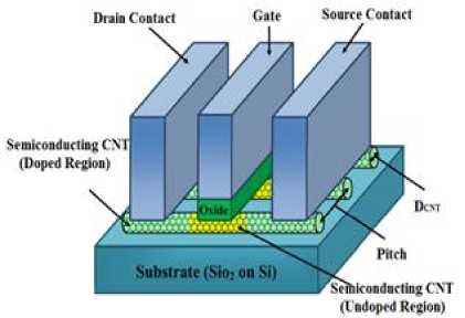
The most essential construction parts in nano devices are Carbon nanotubes (CNT). CNT is a tubular graphite sheet with few nanometers diameter [2, 14]. Based on the number of coaxial tubes shaping the nanotubes, they are categorized as single-wall (SWCNT) or multi-wall (MWCNT) each has distinguished properties for different applications. A single-walled carbon nanotube (SWCNT) can be visualized as a single sheet of graphite which is rolled up and joined together along a wrapping vector Ch = nx ax + n2 a , where [ a , a J , are the lattice unit vectors, and the indices ( n 1 , n 2 ) are positive integers that specify the tubes structure [16]. The method through which the graphite sheet is shaped is defined through a pair of indexes (m, n) named chiral vector (CNT with n-m=3 is metal, otherwise it is semiconductor), [17].
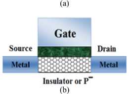
One of the best characteristics of CNT is the ballistic movement of the electron along the tube; hence, the semiconductor CNT may be applied as a channel for transistors [18]. CNTFETs function as common silicon transistors. The CNFET Schottky barrier (SB-CNTFET) is among the different types of CNTFETs. These transistors with a semiconductor nanotube and two metal connections are constructed as source and drain; hence, they have a Schottky barrier in the connection point of metal nanotubes. In this type of CNTFETs the gate controls the injection level of carriers in nanotubes by changing the height of the barrier at metal-semiconductor connection level [19]. Due to their strong multipolar characteristic, SB-CNTFETs are appropriate to be applied at logic CMOSs family. The MOSFET-like CNTFET is another type of CNTFETs with a unipolar behavior contrary to the SB-CNTFET. The source and drain are injected with impurity in an intensive manner and the CNTFET functions based on the generated barrier’s height through the gate potential. The MOSFET-like CNTFET, in the source channel junction of which no Schottky Barrier is applied. This type of CNFET has significantly high ON current, which makes it usable for ultra-high performance digital applications [2, 3]. Both SB-CNTFETs and MOS-CNFETs are applied for high speed design due to their high turn-on current. However, another type of CNFET (T-CNTFET, band-to-band tunneling CNTFET) is applied for low power consumption design based on low turn-on current [2, 20]. Fig. 1 shows these kinds of CNFETs.
Based on what is presented and considering the process and construction of different types of CNTFETs and their performance, the MOSFET-like CNTFETs are applied in this proposed design.
Gate
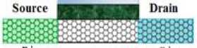
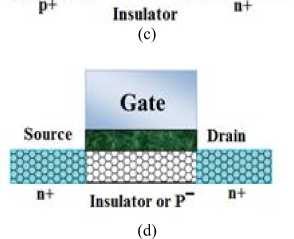
Fig.1. (a) Schematic of carbon nanotube field effect transistor (b) SB-CNTFET (c) T-CNTFET (d) MOSFET-like CNTFET [2, 6, 14]
The threshold voltage of the CNTFETs can be controlled by adjusting the nanotube diameter. The voltage necessary to turn on a CNTFET is called the threshold voltage. The CNT diameter can be calculated as (1).
a 22
Dcnt = — л/ n + nm + m . n
Where, parameter a = 3aa 0 is the carbon to carbon distance and a0=0.142 nm is the length of the carboncarbon bond. The simplified equation is given by (2) [2, 3, 15].
Dcnt = 0.0783V n 2 + nm + m 2 . (2)
Therefore, it is possible to turn on the CNTFET at a required voltage and design the appropriate circuit with better performance. The threshold voltage is given as (3).
majority function[25]. In the circuit illustrated in Fig. 5, a separate dynamic current mode circuit is designed for SUM and Cout output, with functions in a simulation manner [26].
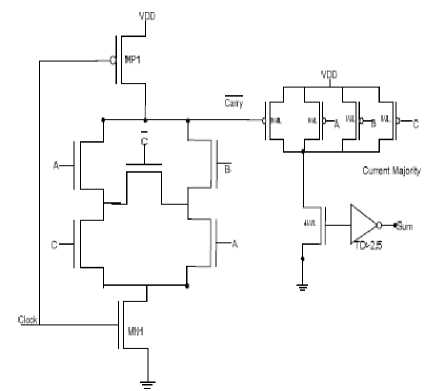
Fig.1. Dynamic CMOS-Bridge current mode full-adder [23]
„ = E g = V3 jv v^ ^ 043
2 e 3 eDCNT DCNT
where v n is the n-n bond energy in the tight bonding model, equal to 3.033 eV, e is the unit electron charge, E is the diameter of CNT measured in nm and is the band gap [21].
In (3), the threshold voltage of a CNT channel is approximated as the inverse function of the diameter.
III. Related Works
In order to have a better performance and lower power consumption in digital computers, researchers have to concentrate on designing full adders with overall better performance. As it is evident, adder is the most important unit in most arithmetic circuits and is recognized as basis of other arithmetic operations [2, 6, 14, 22]. The functionality of some current mode full-adders are reviewed here. In the circuit illustrated in Fig. 2 [23], a dynamic CMOS-Bridge circuit is applied and its SUM output functions are based on current mode logic. In the circuit illustrated in Fig. 3 [24], to construct the primary minority function, a static CMOS-Bridge is applied and the output SUM functions determined through current mode majority function. in the circuit illustrated in fig. 4,
Cout is constructed based on a three input minority function gate and output applying by a current mode
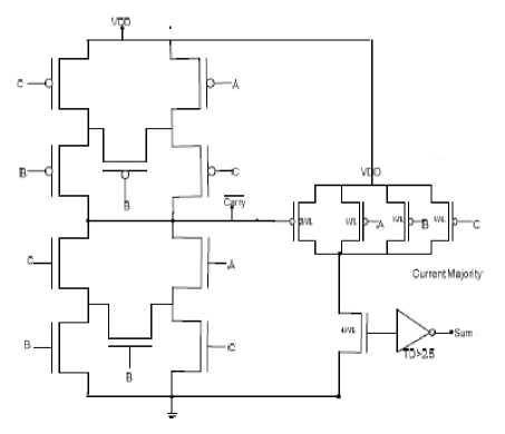
Fig.2. Static CMOS-Bridge current mode full-adder [24]
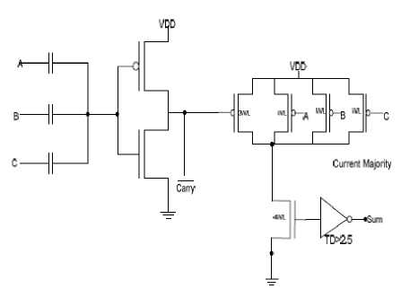
Fig.3. Majority function current mode full-adder [25]
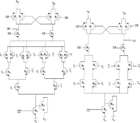
Fig.4. Parallel dynamic current mode full-adder [26]
-
IV. The Proposed Full Adder
A new design for a low PDP in current mod adder is presented in this section. The mean idea is driven from the truth table of a full adder. Every full adder accepts the three a, b and c input signals and generates SUM and Cout as the outputs according to Table 1.
Table 1. The full adder correction Table
|
Input |
Output |
|||
|
A |
B |
C |
Sum |
Cout |
|
0 |
0 |
0 |
0 |
0 |
|
0 |
0 |
1 |
1 |
0 |
|
0 |
1 |
0 |
1 |
0 |
|
0 |
1 |
1 |
0 |
1 |
|
1 |
0 |
0 |
1 |
0 |
|
1 |
0 |
1 |
0 |
1 |
|
1 |
1 |
0 |
0 |
1 |
|
1 |
1 |
1 |
1 |
1 |
In general, these outputs are defined according to (4) and (5):
Cout = ab + ac + bc.(4)
SUM = a © b © c.(5)
Equation (4) can be rewritten as a three input majority function of the (a, b and c) signals, expressed as (6):
Cout = Majority (a, b, c).(6)
Likewise, by expanding (5), (7) and (8) is yield:
SUM = abc + abc + abc + abc.(7)
SUM = abc ( a + b + c ) + abc ( ab + ac + bc +
(8) abc )( a + b + c )( ab + ac + bc + abc ).
Equation (8) can be rewritten as (9), which can be expressed as a three input minority function, expressed as (10).
SUM = NAND ( a , b , c ) • NOR ( a , b , c ) + NAND ( a , b , c )
• ( ab + ac + bc ) + NOR ( a , b , c ) • ( ab + ac + bc ).
SUM = Minority ( NAND ( a , b , c ), NOR ( a , b , c ), ( ab + ac + bc )) •
As observed in Table 2 the gates NAND and
NOR
change status at only one of the inputs situations(shown in table in bold), indicating that this few switches count at these gates output which constitute inputs of the final minority function, reduce the error probability at the output and increase the circuit safety in a significant manner.[27]
Table 2. The NAND and NOR gates’ correction Table
|
Input |
Output |
|||
|
A |
B |
C |
NAND |
NOR |
|
0 |
0 |
0 |
1 |
1 |
|
0 |
0 |
1 |
1 |
0 |
|
0 |
1 |
0 |
1 |
0 |
|
0 |
1 |
1 |
1 |
0 |
|
1 |
0 |
0 |
1 |
0 |
|
1 |
0 |
1 |
1 |
0 |
|
1 |
1 |
0 |
1 |
0 |
|
1 |
1 |
1 |
0 |
0 |
At this stage, the third input of the minority function, in (10) that is resembles (5), which is replaced with (6), thus (11) is yield:
SUM = Minority ( NAND ( a , b , c ), NOR ( a , b , c )
, Majority ( a , b , c )).
Eventually the output can be defined through (12):
SUM = Minority ( NAND ( a , b , c ), NOR ( a , b , c ), Cout ).
The correctness table of the inputs and outputs of all applied gates in this proposed circuit according to (12) are tabulated in Table 3 for better comprehensions.
The design of this circuit structure is modeled according to (12), Fig. 6.
NOR
Fig.6. The proposed full adder circuit
Table 3. Correctness table of the components of proposed circuit
|
Input |
Output |
|||||||
|
A |
B |
C |
2 > 2 ? to ъ |
2 о ? w |
О ? to |
n о e |
^o to 5! § н o 5 N< to A S'? ^ я и 33 о 3" p |
SZ) d 3 |
|
0 |
0 |
0 |
1 |
1 |
0 |
0 |
1 |
0 |
|
0 |
0 |
1 |
1 |
0 |
0 |
0 |
0 |
1 |
|
0 |
1 |
0 |
1 |
0 |
0 |
0 |
0 |
1 |
|
0 |
1 |
1 |
1 |
0 |
1 |
1 |
1 |
0 |
|
1 |
0 |
0 |
1 |
0 |
0 |
0 |
0 |
1 |
|
1 |
0 |
1 |
1 |
0 |
1 |
1 |
1 |
0 |
|
1 |
1 |
0 |
1 |
0 |
1 |
1 |
1 |
0 |
|
1 |
1 |
1 |
0 |
0 |
1 |
1 |
0 |
1 |
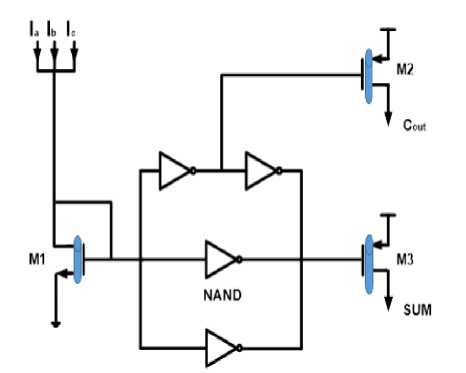
The proposed full adder is implemented through a three inputs majority function, a NAND gate and a NOR gate by applying CNT technology. In this circuit Cout is the same as the three input majority function of (a, b, c), while SUM is the three input minority function of (Cout, NAND, NOR). SUM is calculated in two stages: at the first stage, output is the result of NAND and NOR gates and the three input majority function (Cout) and at the second stage, the logical outputs of the previous stage are assigned to a three input minority function and the final response (SUM) is obtained.
In Fig. 7, the proposed circuit structure is presented in its transistor level with more complete details. It is observed that NAND, NOR and Cout gats can be designed through NOT gate based on CNTFET by only changing the transistors’ threshold voltage, with least transistor. The NAND gate is a NOT gate with high NMOS threshold voltage and low PMOS threshold voltage, while the NOR gate is a NOT gate with high PMOS threshold voltage and low NMOS threshold voltage [24]. It is worth mentioning that this design takes the advantage of a novel structure, demonstrated by equation (12).
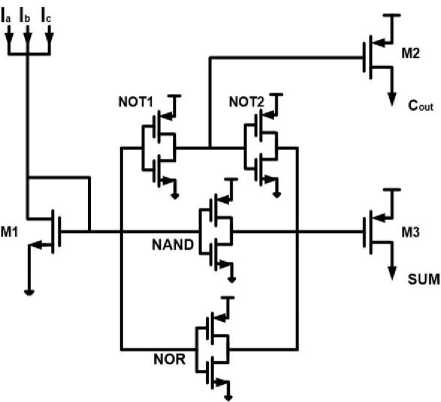
Fig.7. The proposed full adder circuit structure
-
V. Simulation and Comparison
Simulations has been performed on previous current mode full adder designs and then the results are compared with the proposed design. Simulations on all implemented designs has been performed by HSPICE circuit simulator. For simulating CMOS circuits, 32 nm CMOS technology has been used, also for the CNT-FET circuit the recent Stanford University model has been applied to do the simulations. This standard model has been designed for enhancement-mode unipolar MOSFET-LIKE CNTFETs, in which each transistor may include more than one CNT as its channel. The model also comprises a full trans-capacitance network for more accurate dynamic and transient performance simulations [2, 21]. Moreover, this model takes into account a realistic, circuit-compatible CNFET structure and includes practical device no idealities, parasitic, Schottky-barrier effect at the contacts, doped source-drain extension regions, scattering (nonideal near-ballistic transport), inter-CNT charge screening effect, back-gate (substrate bias) effect and Gate and Source/Drain, resistances and capacitances. The model also comprises a full trans-capacitance network for more accurate transient and dynamic simulations. The important parameters of the CNFET model and their related values and a brief description, are tabulated in Table 4.
The model proposed by Stanford University is applied to simulate the circuit based on CNTs with 0.65 V power supply voltage and 320 MHz frequency at room temperature. The time necessity for output to reach 50% of its swing while the input has reached 50% of its swing is named delay and the longest delay is considered as the circuit delay. This proposed circuit has a short critical path to generate SUM and Cout; Thus, its delay is 0.16 nanosecond and the circuit power consumption is 6.4 µW. PDP as the combination of power consumption and circuit speed is a numeral scale to evaluate the circuit efficiency.
pdp of the proposed circuit is 0.74 × 10⁻¹⁵ . t he functionalities of this proposed circuit compared to the previous circuits in terms of delay, power and PDP are expressed in Table 5. Where the proposed circuit the power consumption is lower compared to that of the circuits of Figs. 2, 3 and 4 due to its simpler structure and lower count of nodes, while has lower delay compared to that of the circuit of Fig. 5 due to lower count of transistors and shorter critical paths; Nevertheless, no significant improvement is observed erectly in the delay of the rest of the resources.
Table 4. CNFET Parameters [2,21]
|
Param eters |
Description |
Value |
|
Lch |
Physical channel length |
32 nm |
|
Lgeff |
Mean free path in the intrinsic CNT channel |
100 nm |
|
Lss |
Length of doped CNT source-side extension region |
32 nm |
|
Ldd |
Length of doped CNT drain-side extension region |
32 nm |
|
Kgate |
Dielectric constant of high-k top gate dielectric material |
16 |
|
Tox |
Thickness of high-k top gate dielectric material |
4 nm |
|
Csub |
Coupling capacitance between the channel region and the substrate |
40 PF/m |
|
Efi |
The Fermi level of the doped S/D tube |
6 eV |
|
Lch |
Physical channel length |
32 nm |
|
Lgeff |
Mean free path in the intrinsic CNT channel |
100 nm |
|
Lss |
Length of doped CNT source-side extension region |
32 nm |
|
Ldd |
Length of doped CNT drain-side extension region |
32 nm |
|
Kgate |
Dielectric constant of high-k top gate dielectric material |
16 |
|
Tox |
Thickness of high-k top gate dielectric material |
4 nm |
|
Csub |
Coupling capacitance between the channel region and the substrate |
40 PF/m |
Table 5. Comparison of simulation results
|
Design type |
Main parameters of the circuit |
||
|
Full Adder |
Power(µW) |
Delay(nS) |
PDP (e-15J) |
|
Dynamic CMOS-Bridge |
231 |
0.013 |
3.003 |
|
Static CMOS-Bridge |
285 |
0.014 |
3.93 |
|
Majority function |
301 |
0.014 |
3.214 |
|
Parallel dynamic |
0.00003 |
239 |
0.005 |
|
Proposed |
6.396 |
0.11588 |
0.74131 |
The accuracy of this proposed circuit is observed as the output wave’s form in Fig. 8.
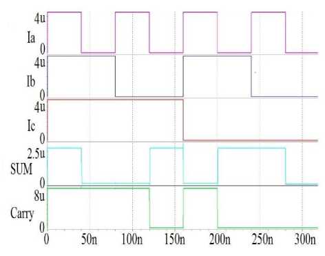
Fig.8. Input and output waves of the proposed circuit
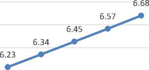
Because temperature is one of the initial comparts in assessment of VLSI circuits, this newly proposed circuit has been simulated subject to 10-50oC range. As observed in Figs. (9), (10) and (11), this design is capable of maintaining its optimal functionality as temperature vary.
6.80
6.60
6.40
о Рн
6.20
6.00
10 20 30 40 50
t emp ( o C)
Fig.9. Circuit power consumption in relation to temperature variation
0.16
0.14
0.12
5- 0.1
0.08
Q 0.06
0.04
0.152
0.10714
0.092721
0.079336
0.02
10 20 30 40 50
Temp(oC)
Fig.10. Circuit delay in relation to temperature variation
0.94712
0.8
0.6
0.4
0.2
0.79939
0.69139
0.60877
0.52997
10 20 30 40 50
Temp(oC)
Fig.11. Circuit PDP in relation to temperature variation
-
VI. Conclusion
In this article, a current mode full-adder circuit based on CNFET enhanced with considerable delay and PDP is proposed, and then it is compared to several samples of current mode full-adder circuits in terms of functionality. In the newly designed circuit the transistors count and critical paths are reduced and the reliability of the circuit is increased. The results reveal that applying CNT and current mode increase circuit speed. With respect to circuit power consumption, reducing the circuit resistance is one of the methods to reduce power. The presented results indicate that the current mode design approach considered is a viable solution for high performance VLSI design in nanotechnology.
References Design of an efficient current mode full-adder applying carbon nanotube technology
- P. Bhattacharyya, B. Kundu, S. Ghosh, V. Kumar, A. Dandapat, “Performance analysis of a low-power high-speed hybrid 1-bit full adder circuit,” IEEE Transactions on very large scale integration (VLSI) systems, 23(10), pp. 2001-2008, 2015.
- M. R. Reshadinezhad, M. H. Moaiyeri, K. Navi, “An Energy-Efficient Full Adder Cell Using CNFET Technology,” IEICE transactions on electronics, NO.95, Vol.4, pp. 744-751, 2012.
- S. A. Ebrahimi, M. R. Reshadinezhad, A. Bohlooli, M. Shahsavari, “Efficient CNTFET-based design of quaternary logic gates and arithmetic circuits,” Microelectronics Journal, Volume 53, Pp. 156-166, July 2016.
- H. T. Bui, Y. Jiang, “Design and analysis of low-power 10-transistor full adders using XOR-XNOR gates,” IEEE Trans. Circuits Syst. II, Analog Digit. Signal Process, 49 (1), pp. 25-30, 2002.
- S. Goel, A. Kumar, M. A. Bayoumi, “Design of robust, energy efficient full adders for deepsubmicrometer design using hybrid-CMOS logic style,” IEEE Transactions on Very Large Scale Integration Systems, 14(12), pp. 1309-1321, 2006.
- M. R. Reshadinezhad, N. Charmchi, K. Navi, “Design and Implementation of a Three-operand Multiplier through Carbon Nanotube Technology,” International Journal of Modern Education and Computer Science, Vol. 7, Iss. 9, pp. 44-51, Sep 2015.
- Z. H. Kong, K. S. Yeo, C. H. Chang, “Design of an area-efficient CMOS multiple-valued current comparator circuit,” IEEE Proc.-Circuits Devices Syst, Vol.152 (2), pp. 151-158, 2005.
- J. T. Butler, “Multiple-valued logic: Examining its use in ultra-high speed computation,” IEEE Potentials, 14 (2), pp. 11-14, 1995.
- A. G. Delavar, K. Navi, O. Hashemipour, “High Speed Full Swing Current Mode BiCMOS Logical Operators,” IJE Transactions, Vol 20 (3), pp. 211-220, 2007.
- N. Weste, D. Harriss, CMOS VLSI Design, 3rd ed., Addison Wesley, 2005.
- M. Rabaey, A. Chandrakasan, B. Nikolic, Digital Integrated Circuits, Second Edition, Upper Saddle River, New Jersey: Prentice-Hall, 2003.
- S. Rahbar Arabani, M. R. Reshadinezhad, M. Hagparast, “ Design of a Parity preserving Reversible Full Adder/Subtractor Circuit,” International Journal of Computational Intelligence Studies, Vol. 7, No. 1, pp. 19-32, 2018.
- G. Gho, Y. B. Kim, F. Lombardi, “Performance evaluation of CNFET-base logic gates,” Proc. IEEE International instrumentation and measurement technology conference. Pp. 909-912, 2009.
- F. Sharifi, M. H. Moaiyeri, K.Navi, “A Novel Quaternary Full Adder Cell Based on Nanotechnology,” I.J. Modern Education and Computer Science, Vol.7, No.3, pp. 19-25, 2015.
- M. H. Moaiyeri , R. F. Mirzaee, K. Navi, A. Momeni, “Design and analysis of a high-performance CNFET-based Full Adder,” International Journal of Electronics, 99(1), pp. 113-130, 2012.
- R. Saito, G. Dresselhaus, M. S. Dresselhaus, Physical Properties of carbon nanotubes, imperial college press, London, 1998.
- P. Avouris, Z. Chen, V. Perebeinos, “Carbon-based electronics,” Nature Nanotechnology 2, v2/n10, pp. 605-615, 2007.
- R. Martel, T. Schmidt, H. R. Shea, T. Hertel, Ph. Avouris, “Single and multi-wall carbon nanotube field-effect transistors,” Applied Physics Letters, Vol.73(17), pp. 24-47, 1998.
- R. Saito, T. Takeya, T. Kimura, G. Dresselhaus, M. S. Dresselhaus, “Raman intensity of single-wall carbon nanotubes,” Phys. Rev.B, Volume 57, Issue 7, pp. 41-45, 1998.
- M. Ahmadi, M. R. Reshadinezhad, “A New High Speed 2n−1 Modular Adder Based on Carbon Nano Tube Field Effect Transistors,” Journal of and Optoelectronics, Vol. 12, pp. 1-8, July 2017.
- Y. B. Kim, F. Lombardi, “A Novel Design Methodology to Optimize the Speed and Power of the CNTFET Circuits,” 52nd IEEE International Midwest Symposium on Circuits and Systems, pp. 1130-1133, 2009.
- S. Heinze, J. Tersoff, R. Martel, V. Derycke, J. Appenzeller, P. Avouris, “Carbon nanotubes as Schottky barrier transistors,” Physical Review Letters, 89(10), pp. 106801, 2002.
- K. Navi, R. Zabihi, M. Haghparast, T. Nikobin, “A Novel Mixed Mode Current and Dynamic Voltage Full adder,” World Applied Sciences Journal, Vol.4, pp. 289 -294, 2008.
- S. Wairya, R. K. Nagaria, S. Tiwati, “New Design Methodologies for High Speed Mixed- Mode Full Adder Circuit,” International Journal of VLSI and Communication Systems (VLSICS), AIRCC Publication, vol. 2, no. 2, pp. 78-98, 2011.
- K. Navi, M. H. Moaiyeri, F. R. Mirzaee, O. Hashemipour, B. Mazloom Nezhad, “Two new low-power Full Adders based on majority-not gates,” Microelectronics Journal, Vol. 40, pp. 126-130, 2009.
- S. R. P. Sinha, N. Tiwari, “Design and Analysis of Dynamic Current Mode Full Adder with reduced Power and Delay,” International Journal of Science and Research (IJSR), ijsr.net, Volume 4 Issue 11, pp. 2383 – 2388, 2015.
- F. Sharifi, A. Momeni, K. Navi, “CNFET BASED BASIC GATES AND A NOVEL FULLADDER CELL,” International Journal of VLSI design & Communication Systems (VLSICS), Vol.3, No.3, pp. 11, 2012.
