Design of near threshold 10T- full subtractor circuit for energy efficient signal processing applications

Author: M.Mahaboob Basha, K.Venkata Ramanaiah, P. Ramana Reddy
Journal: International Journal of Image, Graphics and Signal Processing @ijigsp
Article in issue: 12 vol.9, 2017.
Free access
In recent years, near threshold computing is becoming a promising solution to achieve minimum energy consumption. In this paper, the Dynamic Threshold body MOS (DTMOS) technique is assessed in the context of 10T full subtractor circuit designed to operate in the near threshold region. The performance parameters – Energy, power, area, delay, and EDP were computed and compared with the conventional CMOS (C-CMOS) Full subtractor. The simulations were performed using cadence 90 nm technology with Ultra Low Voltage (ULV) of 0.3V. The results have been shown that the proposed 10T full subtractor circuit with DTMOS scheme achieves more than 18% savings in delay, 26% savings in energy consumption and 39% savings in EDP in comparison with the conventional CMOS configuration and other hybrid counterparts.
CMOS (Complementary Metal Oxide Semiconductor) logic, DTMOS (Dynamic Threshold body Metal Oxide Semiconductor) logic, Energy, full subtractor, Near Threshold, ULV (Ultra Low Voltage)
Short address: https://sciup.org/15015921
IDR: 15015921 | DOI: 10.5815/ijigsp.2017.12.03
Text of the scientific article Design of near threshold 10T- full subtractor circuit for energy efficient signal processing applications
Published Online December 2017 in MECS
As the technology trends to scale down to the nanometer regime with the increase in the demand for portable battery operated devices like laptops, calculators, mobiles, wrist watches and IoT devices, the energy consumption of digital circuits is becoming a major issue [1]. Supply voltage (Vdd) scaling serves as an effective knob for reducing the energy consumption due to the quadratic reduction in the switching energy. Figure 1 shows the values of the VDD with the recent technology trends. It can be observed that scaling of Vdd stalled at 1V. However, this scaling trend of Vdd leads to degradation in the circuit performance. In [3] it was shown that near threshold computing results in energy savings of more than an order of 10× with only 10 times degradation in the performance as illustrated in figure 2.
To achieve maximum computational energy efficiency with acceptable performance, operating digital circuits in the near threshold region (scaling supply voltage Vdd near to VT) is one of the solutions [2, 3]. This is known as Near Threshold Computing (NTC).
Arithmetic operations play a crucial role in most of the signal and image processing applications [12-13]. One of the fundamental arithmetic units is 1-bit full subtractor circuit. Therefore, evaluation of the 1-bit full subtractor circuit performance is required to realize the overall system performance [14-15].
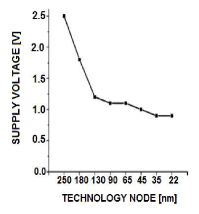
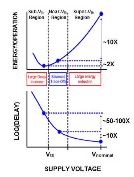
Fig.2.Variations of energy and delay metrics at different operating regions- subthreshold, near threshold, and super threshold. [3].
The basic logic diagram of the 1-bit full subtractor is shown in figure 3 and table.1 shows the truth table for 1-bit full subtractor.
Many full subtractor circuit designs employing different logic approaches have been proposed earlier in the literature. C-CMOS [4], Pass Transistor Logic (PTL) [5], and Transmission Gate (TG) [6-7] logic styles are the most conventional logic designs. Each of the logic designs is having its own advantages and drawbacks with one of the performance parameters-power, delay, and area.
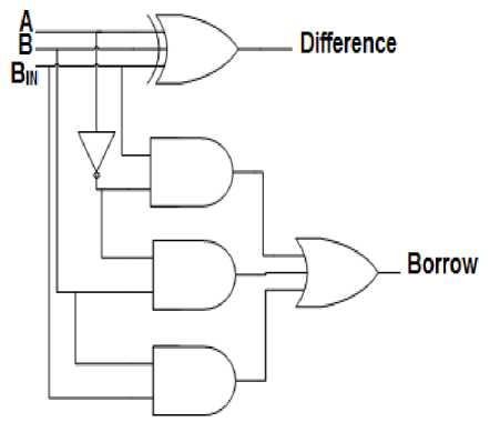
Fig.3. Basic logic diagram of full subtractor circuit
Table 1. Function Table of the one-Bit Full Subtractor
|
Inputs |
outputs |
|||
|
B IN |
A |
B |
Difference |
Borrow |
|
0 |
0 |
0 |
0 |
0 |
|
0 |
0 |
1 |
1 |
1 |
|
0 |
1 |
0 |
1 |
1 |
|
0 |
1 |
1 |
0 |
1 |
|
1 |
0 |
0 |
1 |
0 |
|
1 |
0 |
1 |
0 |
0 |
|
1 |
1 |
0 |
0 |
0 |
|
1 |
1 |
1 |
1 |
1 |
In [8], we have proposed a new full subtractor circuit which was designed with only two XOR gates and one multiplexer gate for area and energy efficient applications. However, these design shows good performance in the super threshold operation (V dd > V T ), but the case differs when V dd scales down to the near threshold voltage. The performance of the circuit degrades because of the exponential increase in delay with the supply voltage scaling [1]. Also because of the reduced output swing, the logic styles like CPL may lead to functionality failure for some input test cases.
The same is the case with our proposed design. The C-CMOS logic is the most optimal design style for subthreshold operation, as it provides full output swing and also more robust against PVT variations than the other logic designs [1-2] but it requires number of transistors which lead to huge power consumption and long borrow propagation paths in the design of full subtractor circuits.
In this paper, a popular body bias scheme known as DTMOS [9] is used along with our most area and energy efficient full subtractor circuit to overcome abovementioned issues in the near threshold region of operation. The remaining part of the paper organized as follows. The proposed full subtractor design methodology is mentioned in section-II followed by results and comparative study in section-III. Lastly in section-IV conclusions were made.
-
II. Proposed Design
The circuit and the logic diagram of the proposed 1-bit full subtractor were shown in figure 4 and 5 respectively. The design of proposed 1-bit full subtractor employs static CMOS logic [4], Pass Transistor logic (PTL) [5] with Dynamic Threshold MOS (DTMOS) scheme [9]. The basic logic design structure of the proposed design is similar to the design proposed by ours in [8] which uses static CMOS and PTL logic. Two identical XOR gates and a multiplexer were used to generate the outputs ‘difference’ and ‘borrow’ respectively. Since the difference block consumes more power, the XOR gates with minimum transistor count are used to reduce power consumption.
Vdd
M5
|
M3 A M6 Vdd M4 M1 gnd B M2 gnd |
Difference M8 Bin M10 Borrow |
B
Fig.4. Proposed 10T full subtractor circuit using DTMOS scheme designed in cadence 90nm technology.
The propagation delay for obtaining the output ‘borrow’ is greatly reduced; as only one multiplexer gate is used for propagation of input borrow (B IN ).
As supply voltage scales down, the performance of the circuit degrades due to the exponential increase in delay. If this supply voltage scaling continues towards the near or subthreshold regime, the degradation in the circuit performance may result in the huge energy consumption [1-2].
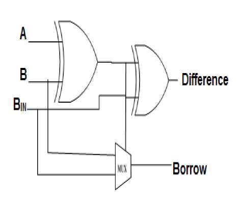
Fig.5. Logic diagram of the proposed full subtractor circuit.
Hence, a DTMOS scheme is employed with this design to improve the energy efficiency while operating in near threshold region.
We have employed DTMOS scheme since it is the most area and energy efficient technique at ULV. Basically, body biasing comes in connecting transistor body terminal to a bias network in the circuit, instead of
Vdd or ground. This body bias can be supplied from an external (off-chip) or an internal (on-chip) source [10].
In DTMOS scheme, the transistor body terminal is tied to the gate input for varying the threshold voltage (V T ) of the device dynamically with respect to the change in gate voltage.
The basic equation which models the impact of body bias on the threshold voltage is given as [8-9].
The parameters γ is the body effect coefficient, ϕ B is the flat band voltage, V SB is the source to body bias voltage and V To is the threshold voltage with zero substrate/ body bias. From equation (1), it is understood that by employing the DTMOS scheme there will be a increase in the VT (When VG=VB=0) and reduction in the V T (When V G =V B =1). This increase of V T reduces the leakage current flow in the transistor which is necessary when the transistor is in OFF state and the reduction of V T improves the switching speed of the transistor which is required when the transistor is in ON state.
-
III. Simulation Results
The proposed full subtractor circuit is simulated and the results were compared with conventional CMOS (C-CMOS) and Dynamic Threshold CMOS (DT-CMOS) full subtractor designs. All the simulations were performed using Cadence 90nm technology with a supply voltage of 300mV and operational frequency of 20KHz.
The comparison of the performance metrics: power, delay, energy and EDP obtained from the simulations are shown in table 2. The comparison plots of performance parameters for different full subtractor designs are shown in figure 6.
Table 2.Simulation Results for different full subtractor circuits designed for NTC
From the comparisons, it is clear that the DT-CMOS design achieves more than 38% and 46% delay savings than the C-CMOS and the 10T designs respectively.
Even though the transistor count of 10T is very less in comparison with the DT-CMOS and the C-MOS designs, but still the 10T design results in more delay. The 10T design may give better performance in the strong inversion region of operation but lags at ULV operation because poor driving capability due to V T drops which may lead to the failure in the functionality of the circuit.
However, the proposed design didn’t achieve much savings in terms of power consumption than the C-CMOS, DT-CMOS designs and also 37% more than our previous design (10T).This is due to the continuous charging and discharging of the body capacitances.
From the comparisons, it can be noticed that the proposed design consumes less energy and EDP than the other designs. This is because of employing the DTMOS
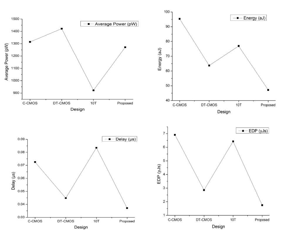
Fig.6. Power, Delay, Energy and EDP comparisons of different full subtractor circuits designed for NTC
But still, the proposed design managed to achieve more than 26% and 39% savings in terms of energy and EDP respectively than the C-CMOS, DT-CMOS and 10T designs. This is because of the comparatively higher delay savings of the proposed design.
The layout of the proposed full subtractor design is shown in figure 7. The obtained timing waveform after post-layout functional simulation of the proposed full subtractor circuit is shown in figure 8.
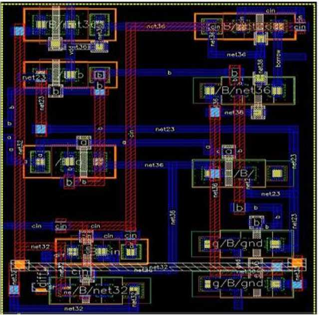
Fig.7. Layout design of the proposed full subtractor circuit in cadence 90nm technology
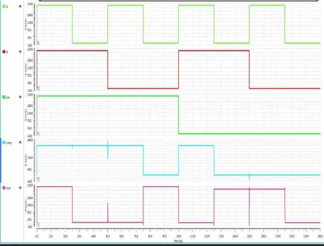
Fig.8. Post-Layout functional simulation waveform of the proposed full subtractor circuit in cadence 90nm technology
It can be noticed that the proposed design with the layout area of 25.36µm2, achieved more than 18% savings in delay, 26% savings in energy consumption and 39% savings in EDP in comparison with the conventional CMOS configuration and other counter parts.
Monte-Carlo (MC) simulations have been performed on 500 samples in order to study the effect of global and local process variations on the energy consumption of the proposed design as shown in figure 9.
The simulations result in 100% yield with a mean (µ) = 57.5623aJ and standard deviation ( σ ) =117.053aJ. Normal Quantile (NQ) plot is also obtained from the simulations and it seems to be reasonable as per the expected distributions across all the samples.
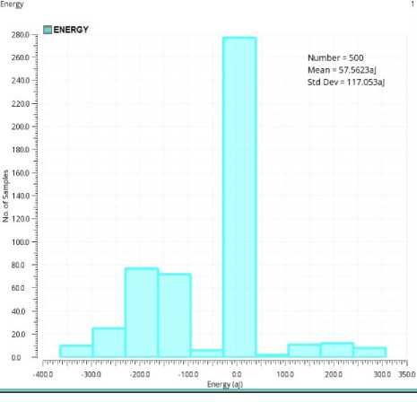
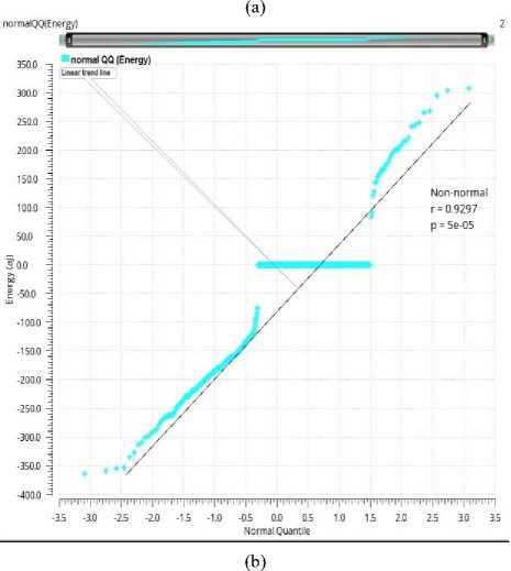
Fig.9. Energy distribution of the proposed full subtractor circuit derived by MC simulations
-
IV. Conclusion
In this paper, a new 10T full subtractor circuit using Dynamic Threshold CMOS (DT-CMOS) scheme is designed for Near Threshold Computing (NTC) to achieve minimum energy consumption. The simulations of the circuits have been carried out using cadence 90nm technology with a supply voltage of 0.3V. The results have shown that the proposed design outperforms the other designs (CMOS, DT-CMOS, 10T) by achieving more than 18% delay savings, 26% energy savings and 39% EDP savings. Hence, the proposed full subtractor circuit can be used as one of the substitutes instead of many Ultra Low Voltage (ULV) subtractor circuits designed for energy efficient arithmetic applications.
References Design of near threshold 10T- full subtractor circuit for energy efficient signal processing applications
- Wang A, Benton.H.Calhoun, and A. Chandrakasan. subthreshold design for ultra low-power systems. 1st edition. Springer : 2006.
- Michael Hbner and Cristina Silvano. Near Threshold Computing: Technology, Methods and Applications. 1st edition. Springer: 2015.
- R. Dreslinski et al., “Near-threshold computing: Reclaiming Moore’s law through energy efficient integratedcircuits,”Proc.IEEE,no.2,pp. 253–266, Feb. 2010.
- Neil.H.Weste and David Harris. CMOS VLSI design- A circuits and systems perspective. 3rdEdition. Addison Wesley: 2004.
- Zimmermann R, Fichtner W. Low-power logic styles: CMOS versus pass-transistor logic. IEEE Journal of Solid-State Circuits, 1997, 32(7):1079-1090.
- Alioto M, Cataldo GD, Palumbo G. Mixed full adder topologies for high-performance low-power arithmetic circuits. Microelectronics Journal, 2007, 38(1):130-139.
- Shams AM, Darwish TK, Bayoumi MA. Performance analysis of low-power 1-bit CMOS full adder cells. IEEE Transactions on VLSI Systems, 2002, 10(1):20-29.
- M.Mahaboob Basha, K.Venkata Ramanaiah, P. Ramana Reddy. Low Area-High speed- Energy efficient one bit full subtractor with MTCMOS. International Journal of Applied Engineering Research, 2015, 10(11): 27593-27604
- Assaderaghi F, D. Sinitsky, S. Parke, J. Bokor, P. K. Ko, and C. Hu, A dynamic threshold voltage MOSFET (DTMOS) for ultra-low voltage operation. IEDM Tech. Dig., 1994, 809–812.
- Kishore.S, Sakthivel R. Low power realization of subthreshold digital logic circuits using Body bias Technique. Indian Journal of Science and Technology. 2016, 9(5),1-5.
- Shih-Fen Huang et.al, Scalability and biasing strategy for CMOS with active well bias. 2001 Symposium on VLSI Technology, 107-108.
- USN Rao, B Raja Ramesh. Adaptive Signal Processing for Improvement of Convergence Characteristics of FIR Filter. IJIGSP, 2013, 5(12):18-25.
- Zhanfeng Zhang,Liyuan Sheng,Wenming Jiang,Shuai Tong,Hua Cao. A New Adder Theory Based on Half Adder and Implementation in CMOS Gates. IJIGSP, 2010, 2(2): 11-17.
- Abdul Sajid, Ahmad Nafees, Saifur Rahman. Design and Implementation of Low Power 8-bit Carry-look Ahead Adder Using Static CMOS Logic and Adiabatic Logic. IJITCS, 2013, 5(11):78-92.
- Shekoofeh Moghimi, Mohammad R. Reshadinezhad. A Novel 4×4 Universal Reversible Gate as a Cost Efficient Full Adder/Subtractor in Terms of Reversible and Quantum Metrics. IJMECS, 2015, 7(11),:28-34.
