Design of PFC converter based on interleave boost

Author: Zhang Siqian, Vanin A., Wang Bao Liang, Wu Liang
Journal: Бюллетень науки и практики @bulletennauki
Section: Технические науки
Article in issue: 6 т.9, 2023.
Free access
Based on the principle of stagger boost PFC, this paper expounds the application value of stagger PFC theory by developing a scientific and feasible scheme and using Matlab simulation. According to the subject requirements, the use of UCC28070 to achieve PFC control function. And learn IC functions. Based on the theory of interlaced PFC, the most suitable electronic device is selected to adjust each part of the circuit. Finally, Solidworks and Protel software were used to draw the radiator and PCB boards, then the prototype was made and debugged, and the final result was obtained.
Boost circuit, pfc technology, energy conservation, environmental conservation, efficiency
Short address: https://sciup.org/14127778
IDR: 14127778 | UDC: 621.314 | DOI: 10.33619/2414-2948/91/41
Проект преобразователя коррекции коэффициента мощности на основе чередования усиления
Приводится прикладное значение теории ступенчатой коррекции коэффициента мощности путем моделирования в Matlab в соответствии с требованиями субъекта. На основе теории чередующейся коррекции коэффициента мощности выбрано наиболее подходящее электронное устройство для настройки каждой части схемы. В программах Solidworks и Protel были выполнены радиатор и платы печатных плат, затем изготовлен и отлажен прототип и получен окончательный результат.
Text of the scientific article Design of PFC converter based on interleave boost
Бюллетень науки и практики / Bulletin of Science and Practice
UDC 621.314
Due to the rapid development of PFC technology, power factor correction PFC pre-regulators have been widely used in primary industrial switching power supplies and household electricity. The traditional single-weight PFC solution is no longer applicable to today's single-phase active
PFC technology, power electronic devices, and power levels that are constantly improving. Due to the increasing power demand, the voltage and current pressure requirements for a single PFC switching device to resist are getting higher and higher, and there are a lot of difficulties in selecting devices, and the current and voltage at some key points of the circuit change very large instantaneously, resulting in conducted EMI and radiated [1].
The interleaved PFC technology has been put into use in recent years, and the interleaved PFC technology actually refers to the power factor correction PFC technology. The application of this technology has brought many benefits, such as reducing the input current ripple and reducing the withstand voltage and current requirements of power devices; the capacity of a single inductor is reduced, and the output power is increased, thereby greatly reducing the entire power circuit [2].
This design is based on the design and development of the power factor correction part of the on-board charging power supply for electric drive vehicles. The main goal is the primary PFC preregulation circuit of the on-board power supply. The interference of the electric vehicle power supply increases the power factor, reduces the amount of harmonics, and makes it more environmentally friendly and green [3].
Parameter Design of Main Circuit Components
Based on the characteristics of the chip and the requirements of the experimental circuit, the parameters of each component of the boost circuit of the main unit can be obtained with the help of relevant formulas. The implementation process is as follows. Based on the chip application manual, the ratio of the input ripple current to the ripple current of a single inductor can be obtained. In the two-phase interactive PFC, it is a function of the duty cycle, because the inductor ripple can be offset by a certain method, so there is no need to worry about a single inductor even if there is a large ripple. Usually, the determination of the boost inductor mainly depends on the maximum ripple current. In the full-cycle input state, the maximum ripple can be determined at the peak of the bottom line voltage. Based on the chip manual, the specific value of the inductance at full load can be obtained [4].
г. _ VOUT - V IN MIN ''/2 _ 390 - 180^ ^^ .
V 390
OUT
K ( D ) = 1 - 2^ = 1 - 2 * 0.35 = 0.462
-
1 - D 1 - 0.35
pou T* 72 * 0.3 3 600 * 72 * 0.3
Vin *П* K ( D ) = 180 * 0.9 * 0.462
_ VN _ min 72 * D _ 18072x0.69
= ML * fs ” 19.96 * 100 k
Under light load conditions, the maximum possible inductance is:
L = 255 цН
Finally choose the average value as the inductance value:
Lmg = LMIN + LMAX = 150цН
Average maximum current through a single inductor:
I = P = 3600 = lu A
Lav 2x n x VMIN 2 x 0.9 x 180
From the above calculations, it can be seen that the final selected single inductance value can withstand a limit current of 11.1A. In order to ensure that the system has good scalability and safety, the actual current withstands value is designed to be 20A. In addition, because it is high-frequency work, so A ferrite core is chosen [5].
Usually, the determination of the output capacitor mainly depends on the actual demand for filtering power frequency ripple:
-
2 x Pout 2 x 3600
C = f IE =---- 47---- *
OUT Vou / - (0.75 x vou т) 2 3 90 2 - (292.5) 2 Ц
For this capacitance, the voltage ripple at the output peak VRIPPLE It can be obtained by the following formula:
V RIPPLE =--------- 2 x P OUT ---------* 12.9V
2n xn x V OUT x 2 fLINEx C OUT
Through the above calculation, we can know that three 1000 uF capacitors that can withstand 450V voltage are finally selected to be connected in parallel.
Selection of power switch tube and output diode. The determination of output diodes and power switch tubes mainly depends on indicators such as peak current, average current, and operating voltage. As far as peak current is concerned, it can be obtained with the help of the following formula, namely:
I PEAK
= (— 2 2°^ --+ ^ I L )1.2 * 30.9A
-
2 x VIN MIN x П 2
As for the average current of the switch tube and the output diode, it can be obtained by using the following formula in turn, namely:
IDS
OUT
n
2 л/2 x V IN MIN ^^^^.

—
16 2 V IN _ MIN
^^^™
3 n x V OUT
* 7.42A
P OUT 3600
1 =----=-----* 4.62A
D V0UT 2 x 390
Through the above calculation, it can be seen that the voltage that the diode and the switch tube need to withstand is 400V. Based on this, it is finally determined that the switch tube is selected as FDH44N50, and the diode is selected as DES12x31-06C.
PFC control circuit design. Clock Setting and Maximum Duty Cycle Clamping [6].
RR
The role of the resistors RT DMX is to set the operating frequency of the chip and the maximum output duty cycle, which can usually be obtained in sequence with the help of the following formulas:
„ 7.5 x 10 9 Q 7.5 x 10 9 Q
R„ т =-------==
RT f100
In order to effectively protect the switching tube, the maximum duty cycle generally does not exceed 0.97, R = R /2 x D — 1) = 68.1Ш.
DMX RTMAX
-
1. Front-end and back-end sampling network
R 、 R
A B meaning of the representative is the front and rear end voltage divider network used for voltage sampling. In order to control the input current of VSENSE and VINAC as much as possible and reduce the power consumption of PFC, generally choose a larger resistance RA , in series in the system circuit , R, = 3.2 M Q , R
A B The output voltage can be effectively adjusted:
V REF
Rb = -2-
V
OUT
—
-A- = 3 x 3.2 M ^ 24.9 k ^
V REF
In order to effectively protect the circuit system, it is necessary to set the threshold voltage of the overvoltage protection OVP:
Op = 3.18 R + R = 3.18
RB
3.2 M + 249k . 412 V
24.9 k
In order to reduce or even eliminate the influence of high-frequency clutter on the sampling R signal, it is usually necessary to BA small capacitor is connected in parallel for filtering processing. Based on the actual working environment and the frequency response of the capacitor, the setting is 220pF.
The design method of voltage loop compensation is usually constructed on the basis of the compensation method designed by Llgd-Dixon. In this research, the design will be based on the chip manual [7]. The main function is to offset the low-frequency ripple, and try to ensure that the low-frequency ripple is controlled at 3% of the output voltage, so as to achieve higher transmission efficiency and reduce the current distortion rate. Regarding the gain of the voltage amplifier and the voltage divider network, the following formula can be used to calculate:
gm v = 70 p s
H = VRF =---- 0.0077
V 390
V OUT 390
Z , V . The main
In terms of output impedance O , its main role is to offset the output ripple ripple role is to control its effective output voltage ratio of 20% (A VA0) Impact. And about the feedback capacitor CPV can be determined by the following formula.
A VA0 = 3.2V
_ A VA_ 0 0.03 _ 3.2 x 0.03 _
= VnpplHgms ” 12.9 x 0.0077 x 70 p =
2. 7 x 2 fLINEZ o
2 7 x 2 x 47 x 13.8 k
~ 124nF
f ,
Further, the crossover frequency of the voltage loop can be obtained cv
P f, = H x gms x------------—OUT------------« 33.26Hz cv V nxA Vao x j 4n2 x C0UT x Vout x CPV
R
Voltage loop compensation resistor ZV Usually placed at the frequency across which the
C The main function of is to increase the gain of the voltage loop compensates for the capacitor ZV voltage loop, and the two can usually be obtained by the following formula:
RZV
33kΩ
С =
ZV
cv PV
2 n x f CV x R.
— «1.5pF
ZV
Connect the PKLMT pin externally to R R ,It can effectively adjust the current limit comparator inside the system. Based on the chip manual, this design is set to 4V. R
V S x R PK 1
4 x 3.65 k -------» 7.5k Q
6 - 4
The default is 3.65k, then PK 2 REF S
At present, there are mainly three kinds of current transformers commonly used in experiments, namely: CS4050V-01L, CS4100V-01L and CS4200V-01L. The principle mainly depends on the primary current frequency. Based on the selection manual, the CS4200V-01L R transformer was finally determined.Transformer sense resistor S . The determination usually depends on the reference voltage VS
, In this design, the reference voltage is set to 4V, and a 10%
R margin is left here, and then the S
,
R s =
0.9 x V x NCT 0.9 x 4 x 200
------------ = ----------- ~ 23.1 Ы .
I PEAK
30.9
In addition, to ensure that the transformer achieves volt-second integration at the highest duty R cycle, it is usually necessary to construct a reset network, resistor R The main function of is to ensure the reset of the transformer, which can be obtained based on the following formula:
о > Rs x Dmax 23.7 x 0.97
R„ ^--------=---------~ /50^
R MAX .
Because the UCC28070 realizes the synthesis of the inductor current by collecting the current R of the switch tube, usually a resistor is connected to its RSYNTH terminal syn It is used to set the current, which can be obtained with the help of the following formula:
24.9
200 x 255 ^ x--- 24.9---
R^ = ----------24.9 + 3200 ^ i80k Q
SYN 23.7
Connect the output of the multiplier to a resistor R , It is used to reasonably set the linear region of the multiplier, which can usually be obtained with the help of the following formula:
= 17 X 10 - 6 x Vinac ( Vvaomax - ) 17 x 10 — 6 X 1.5 x ( 5 - 1) =
K vff 1.156
|
P in ( max ) |
= L^ = Ux^ = 4304w n 0.92 |
P
I = 2 x -(-max- = 2 X 4304 = 47.8A in(pk) V 180
0.5 x I x R„
R =---- ink---S =45k Q
IMO
N CT x 1 IMO
Regarding the switching frequency of the PFC current loop, the general range is between 1/10-1/6. In this design, by combining the actual needs and the working environment, the final choice is 1/10, in order to effectively compensate the current loop, need to know the power stage gain Gps of the current loop, select Rzc, Czc, Cpc as follows:
GPSC
v R x---
OUT x S x -KJ NCT
2 n x |Q x L AVG x V RAMP
390 x 23.7 x —
100 k
2 n x x 150 u x 4
« 1.2
gm is the trans conductance current amplifier gain:
gmc = 100 ^ s
R ZC =--------- gm c x GPSC
« 9.1k Q
® 2.2nF
ZC r
2n — x R r
10 ZC
CPc =------- « 330pF
2 n — x R
-
2 ZC
Soft start and frequency dithering mode setting
Ct
-
1. Soft start. Usually a capacitor is connected to the SS pin SS , for soft start time SS In this design, by combining the actual needs and the working environment, the final choice is 0.2s. Regarding the determination of the capacitance, the calculation formula is as follows:
-
2. Frequency jitter setting (reduce EMI). Based on the chip manual, it can be learned that the variable frequency mode can effectively reduce EMI 。 . External R C Used to set frequency jitter amplitude and rate. For this design, use the default dither settings:
~ 10 ^ A x 0.2 s
C о = « 1 n F
SS 2.25 V
fDM = 30kHz , / d R = 10kHz
The corresponding resistor and capacitor settings are: Rrdm = 31.6Ш CCDR = 220pF .
Regarding the driver of Mosfet, MIC4422 IC is used, which is a low-power driver chip, of which 1 is the power supply pin (VS), 2 is the input pin (IN), 3 is the empty pin (NC), 4 5 and 5 are ground pins (GND), and pins 6 and 7 are output pins (OUT) (Figure 1).
The power supply is 12V, and the purpose of connecting an external 1uF capacitor is to stabilize the voltage. In addition, a 0.1uF bypass decoupling capacitor is added to eliminate voltage glitches. Based on the principle of reducing switching loss, the steeper the front and rear edges of the driving waveform, the better, and the driving source is provided by a stable voltage [8]. However, as far as conventional switching devices are concerned, wiring inductance is very likely to occur, causing failure of the drive, which will affect the stability and safety of the circuit system. In order to properly solve the above problems, it is usually necessary to connect a resistor in series with the gate of the MOSFET to ensure that the oscillation damping is within the specified range. However, the addition of resistance creates a new problem, that is, it may affect the voltage characteristics of the drive to a certain extent, reducing the drive current, making the front and rear edges steeper, and significantly increasing the loss [9]. Therefore, the added gate resistance should not be too large as much as possible, just to reduce the oscillation. Combined with the actual situation, the driving resistance of 3.3 is selected here. Because there is a junction capacitance between the gate and source of the MOSFET, the junction capacitance will be charged as long as the system is powered on. In order to avoid damage to the MOSFET due to excessive junction capacitance, a discharge resistor needs to be connected in parallel between the gate and source. According to engineering experience, select a value of 10k. Relay protection circuit in order to ensure the reliability, safety and efficiency of the circuit, the primary circuit is usually controlled by means of a relay. The general circuit diagram is shown in Figure 2 below.
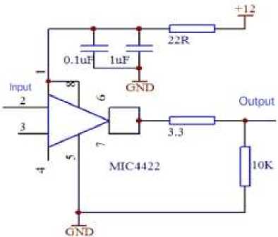
Figure 1. MIC4422 drive circuit
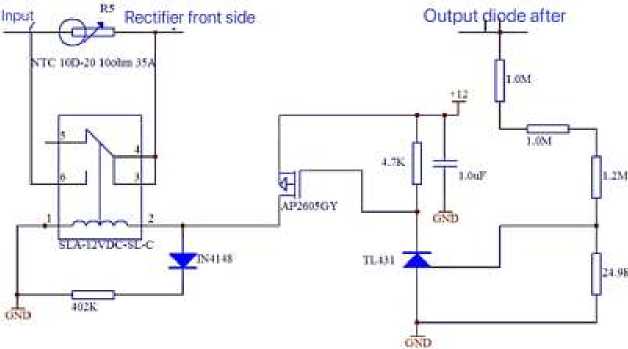
Figure 2. The working principle and process are introduced as follows
-
1. TL431 is a shunt regulator integrated circuit. It is mainly composed of the following parts: output switch tube, voltage comparator and 2.5V reference voltage source, etc. If the input voltage is lower than 2.5V, the system will be in the disconnected state. When the input voltage is equal to or exceeds 2.5V, the system will operate normally. Here use TL431 to form the relay control circuit.
-
2. As shown in Figure 2, before the UCC28070 is officially running, the system will use a negative temperature coefficient resistor to control the current. If the output of the main circuit is 324V, the voltage divider network will be assigned a 2.5V comparison voltage input to the TL431, which will immediately start the working mode, and a P-channel enhanced MOSFET is connected to the output terminal. The power supply is 12V. At this time, the MOSFET is turned on. Based on the above figure, it can be known that the relay pulls in, which will change the current flow direction at the input side of the main circuit, thereby reducing system loss.
-
3. When the output voltage drops, the TL431 will be interrupted, the MOSFET will also stop working, and the relay will also be disconnected. At this time, under the action of the inductive effect, the relay coil will generate current, so a discharge circuit is required, otherwise it will be damaged system. The solution is to form a discharge circuit on the relay coil with the help of diodes and resistors [10].
As far as the auxiliary power supply is concerned, its main function is to provide a +12V power supply for relays and MOSFETs. The general circuit diagram is shown in Figure 3-6 below.
Connect a +15V switching power supply to output +12V voltage. When the output voltage is greater than +12V, use resistors to divide the voltage to form a voltage not lower than 2.5V. In this case, TL431 will be connected immediately, and then the voltage of the triode will be lowered, causing the triode to stop running. And then make +15V power supply interruption. And when the output is less than +12V, TL431 will interrupt the operation, the base voltage of the triode will rise to 15V, and then the output will increase. The above is a simple triode voltage regulator circuit. In order to reduce or even completely offset the electromagnetic interference, it is necessary to design a filter circuit. The approximate circuit diagram is shown in Figure 4 below.
TIP29
15V / \ -12
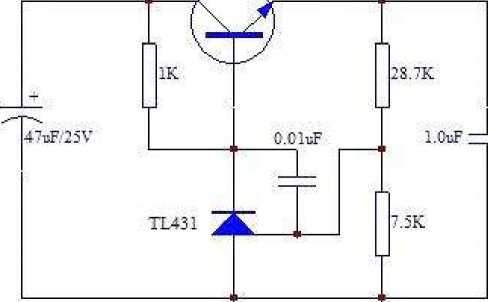
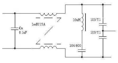
Figure 3. The working principle is as follows Figure 4. The filter circuit
As far as the filter circuit is concerned, it is mainly composed of the following parts: namely, a resonant filter, a common mode inductor, an x capacitor, and a y capacitor. Based on lookup table selection: C x =0.1 p F , C Y =0.01 p F , L = 1mH
The determination of the resonant filter is mainly determined by the frequency to be filtered out. In this design, the switching tube is 100k, and then it can be seen that the clutter is also 100k. Take C = 0.1 p F , Then the resonant inductance can be obtained, namely:
L = —Д^=25рН
4n2 f2 C
s
In this study, for the PFC of the interleaved boost, the simulation analysis was carried out with the help of matlab software. When performing simulation analysis, the relevant parameters usually need to be known in advance and meet certain requirements. Here the simulation time is 0.5s. AC input Vin=220V,output 400V, switching frequency 100kHz, load resistance 50 (3600W), inductance 150uH, output capacitance 2700uF, these parameters are obtained from the previous analysis and calculation.
Based on the above parameters, the obtained simulation results are shown in Figure 5 below.
Т. 9. №6. 2023
Simulation waveforms of inductor interleaving ripple and output diode ripple. Based on the content in the above figure, it can be known that under the conditions of voltage regulation and unity power factor correction, the interleaved boost PFC can reduce the output ripple by 50%, effectively reducing loss and cost, and reducing EMI Figure 5-8.
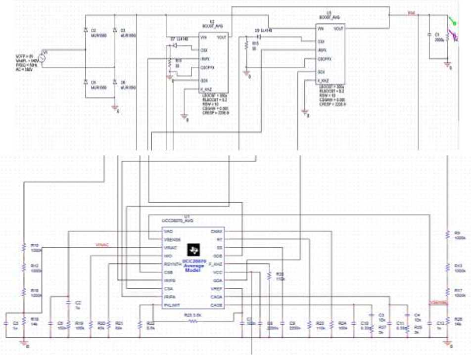
Figure 5. Input and output voltage simulation waveforms
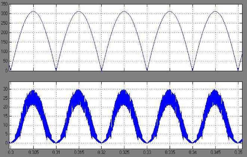
Figure 6. Input voltage and current simulation waveforms on the rear side of the rectifier bridge
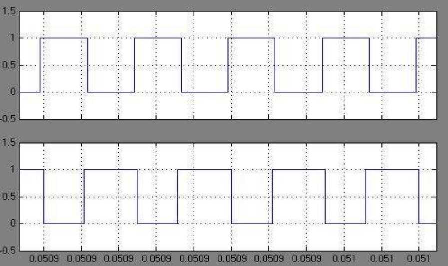
Figure 7. Interleaved 180° pulse waveform
Figure 8. Simulation waveforms
References Design of PFC converter based on interleave boost
- Wang W. et al. An archived dataset from the ECMWF Ensemble Prediction System for probabilistic solar power forecasting // Solar Energy. 2022. V. 248. P. 64-75.
- 周玉婷, 吴羽, 任小永, 陈乾宏, & 张之梁. 基于改进恒导通时间控制的临界连续导通模式 Boost 功率因数校正变换器 //电工技术学报. 2021. V. 36. №20. P. 4329-4338.
- Zhang Chenyu, Wu Yunfeng, Chen Zhangyong, Tang Yuanhong, Zhang Changhua. Capacitor Series Interleaved Parallel Buck PFC Converter with High Power Factor // Chinese Journal of Electrical Engineering. 2019. V. 39. №17. P. 5205-5215.
- Chen Lei. Application Research of GaN HEMT Devices in High Frequency PFC Power Converter. Yanshan University, 2019.
- Xie Lingling, Gong Renxi, Li Shiyong. Dynamic characteristics analysis of photovoltaic power generation maximum power point tracking interleaved parallel Boost converter // Chinese Journal of Electrical Engineering. 2013. V. 33. №06. P. 38-45.
- Han Zhi. Research on High Power Factor and High Efficiency Multi-channel Interleaved Parallel DCM Boost PFC Converter. Southwest Jiaotong University, 2020.
- Xijun Yang, Pengsheng Ye, Hailiang Miao, Huaigang Lei. Realization of Single Phase Double Parallel Interleaved Boost PFC // Power Electronics Technology. 2004. №02. P. 8-9.
- Chang Jianjun. Research on single-phase Boost power factor correction technology. Nanjing University of Aeronautics and Astronautics, 2005.
- Hu Q., Lu Z. A novel step-up VRM - Two-phase interleaved coupled-boost converter // 2006 37th IEEE Power Electronics Specialists Conference. IEEE, 2006. P. 1-5.
- Fu Xunbo, Li Jianlin, Li Zhengmin, E Chunliang. Implementation method of interleaved Boost PFC circuit phase-shifting drive signal // Power Electronics Technology. 2007. №06 P. 83-85.
