Design of Quantum Dot Cellular Automata Based Parity Generator and Checker with Minimum Clocks and Latency

Author: Prateek Agrawal, S.R.P.Sinha, Neeraj Kumar Misra, Subodh Wairya
Journal: International Journal of Modern Education and Computer Science (IJMECS) @ijmecs
Article in issue: 8 vol.8, 2016.
Free access
Quantum-dot Cellular Automata is an alternative to CMOS technology for the future digital designs. When compared to its CMOS counterpart, it has extremely low power consumption, as there is no current flow in cell. The methodology of parity generator and checker is based on the parity generation and matched it at the receiver end. By using the parity match bits, the error in circuit can be sensed. In this paper, novel parity generator and detector circuit are introduced. The circuit is designed in single layer, minimum clock and minimum latency, which is achieved in QCA framework. The proposed circuits are better than the existing in terms of clock cycle delay, cell complexity and clock cycle utilize. The simulation of presented cell structures have been verified using QCA designer tool. In addition, QCA Probabilistic (QCAPro) tool is used to calculate the minimum, maximum and average energy dissipation aspect in proposed QCA circuit. Appropriate comparison table and power analysis is shown to prove that our proposed circuit is cost effective.
Quantum-dot cellular automata, Error control, Nano-communication, Parity generator, Parity checker, low power
Short address: https://sciup.org/15014889
IDR: 15014889
Text of the scientific article Design of Quantum Dot Cellular Automata Based Parity Generator and Checker with Minimum Clocks and Latency
Published Online August 2016 in MECS DOI: 10.5815/ijmecs.2016.08.02
QCA has emerged as a promising technology for nanoelectronic application. Its major advantages like faster speed, smaller size, and lower power consumption have attracted the attention of many researchers. QCA has overcome the physical limitation of traditional CMOS technology, first introduced by C. S. Lent et.al in 1993 [1]. Recent research shows that QCA has faster-switching speed, high packing density, and operate at room temperature. It is the transistor less-technology in which logic levels are described by the configuration of electrons in the quantum dot [3]. There are two approaches in the QCA research area, Physical design and algorithmic design [1]. Among both, an algorithmic approach is an important aspect of the large systems as well as for high-level designs.
In communication system, we are more concerned with detecting and correcting the errors as data are corrupted due to the unwanted noise, which is added to the communication channel. Hence, parity is a concept, which technique is widely used to detect an error in the receiving message [13]. The parity bit is an extra bit added to the data in order to make the number of 1s either even or odd. In this paper, we are focusing on even parity everywhere. We have proposed parity generator (PG) circuit to generate the even parity at the transmitter end and parity checker (PC) circuit to verify the even parity at the receiver end.
The International Technology Roadmap for Semiconductor (ITRS) has proposed some alternative technologies that will replace the CMOS Technology [5]. QCA is one of them, in which quantum dots are used for computation, hence, it provides outstanding energy efficiency, high density and fast computing device [8].
This paper presents the parity generator and checker circuits using QCA framework. The proposed circuit work is (1) Parity generator circuit consumes only half clock pulses. (2) Energy estimation is carried out for PG and PC circuit. To the best of our knowledge, least latency is achieved in the proposed design.
This paper is organized as follows. Section II gives the brief explanation about the background of QCA, includes QCA clock, logic gates (majority voter, inverter) and concise description of kink energy. In the same section, the theory of calculating the power dissipation along with the design rules is summarized. In section III, the background study related to PG and PC is carried out. The proposed circuits of parity generator and checker are well-depicted in section IV. The thermal layout of the proposed circuit is also demonstrated in the same section. Section V compares the obtained results from the preexisting ones. This is followed by section V, where this paper is concluded.
-
II. Basic Concept Related to QCA
In this section, brief overview about QCA, and layout design rules is presented.
-
A. QCA in brief
The fundamental element of this paradigm is a quantum-dot. This section begins with the basic QCA cell which is squared like structure with four quantum dots located at each of its corners as shown in Fig. 1 (a). Two electrons are released to charge the cell which tunnel through to the neighboring cell, but they are incapable of leaving the cell boundaries [2, 8]. Due to columbic repulsion, two electrons tend to occupy the farthest possible distance [6]. There occur two such possible conditions and according to the position of the electron, polarization of the cell is defined. Polarization is denoted by P, P=0 denote the null state, P = +1 denotes the state ‘1’ as shown in Fig. 1 (b) and P = -1 denotes the state ‘0’, shown in Fig. 1 (c).
When two cells are placed near each other, the polarization of one cell will be influenced by the polarization of another cell [10]. Arranging the cells in a row as shown in Fig. 2 results in a QCA binary wire, which transmits the information from one end to other. Fig. 2 (a) and 2 (b) shows the wire transmitting binary ‘1’ and binary ‘0’ respectively. There can be two types of wire based on the type of cell used. As shown in Fig. 3, vertical line represents the ordinary wire (900) and horizontal wire representing the rotated wire (450). The main advantage of using the rotated wire is that the two wires are crossed without intervening the signal of each other.
-
B. Fundamental Gate
There are two fundamental gates in QCA paradigm. These gates are used to construct the layout.
-
(i) QCA Inverter
State inversion mechanism in QCA is performed by diagonal arrangements of two cells as shown in Fig. 4 (a). In this manner input signal is inverted via electrostatic interaction between two diagonally connected cells. QCA robust inverter using seven numbers of cells is another way to design an inverter, depicted in Fig. 4 (b)
-
(ii) QCA Majority Voter (MV)
As it is depicted in Fig. 5, representing (a) majority ‘1’ and (b) majority ‘0’, the main structure of QCA nanotechnology consists of five gates also known as Von-Neuman neighborhood structure [14]. Three of the side cells acts as the input and the fourth one is reserved for output. The middle cell which is a device cell will be affected by the similar impacts of the three input cells. The logic equation of majority gate is as represented by equation 1. By fixing one of the inputs to the +1 and -1, two input OR (equation 2) and two input AND gate (equation 3) is obtained respectively.
M (A, B, C) = AB + BC + CA(1)
M (A, B, 0) =A.B(2)
M (A, B, 1)=A+B(3)
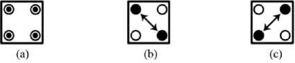
Fig.1. Quantum-dot cell polarizations (a) Empty cell, (b) “1” polarity, (c) “0” polarity
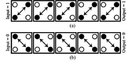
Fig.2. QCA wires: (a) transmitting “1”, (b) transmitting “0
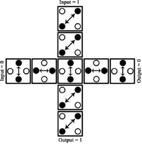
Fig.3. A crossover with rotating cells
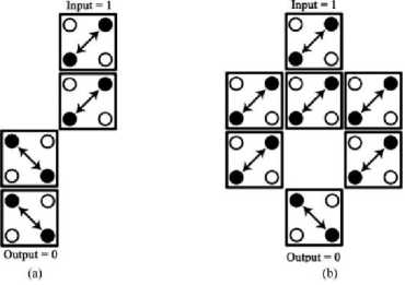
Fig.4. QCA inverter (a) Smaller robust inverter (b) A robust inverter
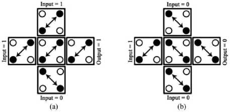
Fig.5. QCA Majority Gates: (a) Majority “1” (b) Majority “0”
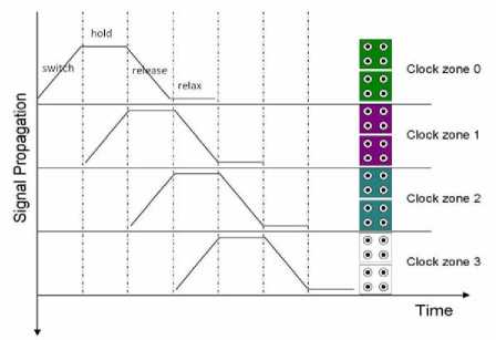
Fig.6. QCA clocking concept
-
D. Kink Energy Calculation
Kink Energy, Ek has a significant role in calculation of power and energy. It is described as the difference between the energy states of two consecutive cells and it depends on the spacing between the two cells and the dimension of the cell but does not depend on the temperature [16]. The columbic interaction between two QCA cells is shown below.
C. QCA Clocking
Clocking in the QCA serves mainly two purposes, first to control the information flow, particularly data transmission through QCA circuits and second to supply the power to the automation [11,12]. Another important application of QCA clock is that it provides the short term memory of the adjacent cells. QCA circuit is organized into four clock zones such as clock 0, clock 1, clock 2 and clock 3. Each clock zone is 900 out of phase to successive clock zone. Each clock zone has its own four states, Switch (low to high), Hold (high), Release (high to low) and Relax (low). Fig. 6, shows the four stages of the clock. Electrons start tunneling between the dots when the clock signal is held high. During the Switch phase, the inter-dot barrier is slowly raised, and the QCA cell is established down to one of the two polarization states as forced by its neighbors. The interdot barrier is held high throughout the Hold phase, which resists the electron tunneling and therefore maintains the current ground polarization state of the QCA cell. The inter-dot barriers are lowered, and the excess electrons gain mobility till the Release and Relax phase respectively.
1 Q 1 Q 2 Q 1 Q 2
E =--= k----
4n e0er r r k = 9 x10⁻⁹
Q1 and Q2are electronic charges, hence E is defined as
23.04 x 10 - 29
r
Hence, based on equation 5, for different values of r we can have the energy variation. Table-1 shows the kink energy calculation for different values of displacement. The energy - displacement curve is neatly depicted in Fig. 7.
Table 1. Kink energy calculation
|
Displacement |
Kink Energy |
|
1 |
23.0 x 10⁻²⁰ |
|
1.2 |
19.2 x 10⁻²⁰ |
|
1.4 |
16.5 x 10⁻²⁰ |
|
1.6 |
14.4 x 10⁻²⁰ |
|
1.8 |
12.8 x 10⁻²⁰ |
|
2 |
11.5 x10⁻²⁰ |
|
2.2 |
10.4 x10⁻²⁰ |
|
3 |
7.6 x10⁻²⁰ |
|
4 |
5.7 x10⁻²⁰ |
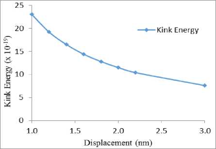
Fig.7. Kink energy vs displacement graph.
-
E. Estimation of Power in QCA
A brief description to find out the power in QCA is provided by equation 6. Since it promises very low power consumption, even traditional i.e. kT [7]. QCAPro tool is used to calculate the power, which works on the model described by equation (6)
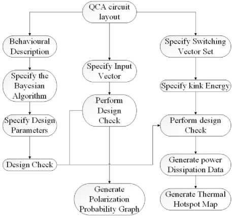
Fig.8. Design flow for the QCA Pro tool.
P total
dE h d - - h- d -
— = -(— Г).Х + — Г.(— X)
dt 2 dt 2 dt
Where λ is the coherence vector and is the threedimensional energy vector. We are more concerned with the second term, which represents the instantaneous power dissipated. Design flow for QCAPro tool is very well depicted in Fig. 8. QCAPro tool makes use of the layout file generated from QCA Designer [17, 19]. Using this layout file, this tool goes through the rapid design check, which tests the value of outputs for all possible values of the inputs. If any error is detected, QCAPro produces the error message and also generates the layout files for all the false states for which the designed circuit is failing to generate the expected output [4]. Hence, it can be inference that design checking is an essential to condition to generate the thermal hotspot map as well as to calculate the power dissipation.
-
F. Design Rules
In the QCA approach, cells are assumed to have a width and height of 18nm and diameter of quantum dots is assumed 5nm. Cells are placed near each other at a distance of 2nm, having the distance of 20nm between the centers of two adjacent cells. Since there is propagation delay between adjacent cells, there is a maximum limit of cell count in a clock zone. [18]. Accordingly, an uninterrupted signal can transmit up to 28 in 900 cells and 27 in 450 cells at a clock rate of 1 THz. These numbers of cells vary according to the operating frequency of QCA circuit.
-
III. Background study
Recently, large amount of work has been done in literature, establishing the circuit in QCA framework. Meanwhile few work is reported on the circuit of parity generator and checker [13, 15, 21, 22, 23], among which most of the work is not cost efficient in terms of clock cycle delay, complexity and area. Gurmohan singh et al. [15] proposed a even parity generator, but circuit utilize 1.75 latency, 87 cell complexity and 0.10µm2 area. Firdous ahmed et al., [22] presented parity generator and checker in QCA framework. These circuits of even parity generator utilize parameters such as 64 cell complexity, 2.75 latency and 0.09 µm2 area. The circuit of even parity checker utilize 94 cell complexity, 1.75 latency and 0.11 µm2 area. Finally existing work have some pros and cons. However, most of the circuit utilizing more QCA primitives such as cell complexity, latency, clock utilize and area. The performance metrics of recent existing designs are drawn by Table 1.
Table 2. Existing work on parity generator and checker
|
Circuit |
Cell count |
Clock utilize |
Latency |
Area µm2 |
|
|
[15] |
4-bit even parity generator |
87 |
7 |
1.75 |
0.10 |
|
[22] |
3-bit even parity generator |
64 |
7 |
2.75 |
0.09 |
|
[22] |
4-bit even parity checker |
94 |
12 |
175 |
0.11 |
-
IV. Design of Error Control Circuits of the Proposed Parity Generator and Checker
In this section, we design the error control circuit such as parity generator and checker. In sub-section A, we propose cell layout of parity generator. Sub-section B design a cell layout of parity checker. The simulation result is presented in sub-section C. Finally, the estimation of energy dissipation related to parity generator and checker are described in sub-section D.
-
A. Parity Generator Circuit
When binary data is transmitted in communication systems, data may get corrupted due to noise, such noise can alter the binary digits from 0s to 1s or vice versa. An extra bit is added at the end of the binary data which indicates whether the no. of transmitted bits have even no. of 1s or odd no. of 1s. Thus, this extra parity bit helps in determining the error. This parity bit is generated by performing the XOR operation between the input bits. Let there be three message bits A, B and C, the parity bit will be generated using the following algorithm where the Boolean equation is successfully replaced by the majority expression as in equation 7. The truth table for generating the expression of P is shown in Table 3. From the truth table, it can be seen that when the number of 1s in message signal is odd, then the value of P is 1 otherwise, P = 0. To generate the parity bit EXOR operation is performed between all the three message signals.
Table 3. Truth table of even parity generator
|
3-bit message |
Parity bit generated |
||
|
A |
B |
C |
P |
|
0 |
0 |
0 |
0 |
|
0 |
0 |
1 |
1 |
|
0 |
1 |
0 |
1 |
|
0 |
1 |
1 |
0 |
|
1 |
0 |
0 |
1 |
|
1 |
0 |
1 |
0 |
|
1 |
1 |
0 |
0 |
|
1 |
1 |
1 |
1 |
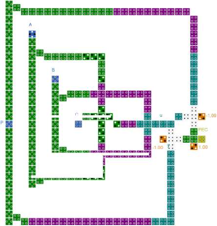
Fig. 9 shows the cell layout of the PG, where the cells with blue color represent the input cells and output is taken from the yellow color cell. Here novelty of this circuit is that the output is achieved using a minimum number of clocks, only three clock pulses are used in the proposed PG circuit. The simulation results of PG are successfully achieved using QCA Designer tool and the results of truth Table 3 is verified, which is neatly shown in Fig. 10. Only clock 2 is shown in the simulation waveform since the output cell is assigned clock 2 in the proposed design. It is seen that the output of PG is received after half unit delay, hence, the latency of our circuit is only half.
P = A Ф B Ф C
= ABC + ABC + ABC + ABC
=(AB+BC+AC).c+(ab+bC+aC).c+(ab+BC+CA)(ab+bC+Ca)=m(A,B,C).c+m(a,b,C).c+m(A,B,C).m(a,b,C)=m(M(A,B,C),m(a,b,C),c)
A
56”® №№№№№■№
M 1ЕЕ1^ыю1®л™™^Н
В
LЙJ1 ЬЖу |*X1J i11g111t^jy ^^B E^t3 ^^E3 ^^^3 Е^^З Е^ЕЗ ^^^3 ^^^3 ^^^3 E^E3 ^^^3
ЕЙ $?®
ВПК® ::
ioi^E^eI^q^q^e^q^q^e^eqq^q^e г"»~] ^^g ^^з ^^з ^^3 ^^3 ^^3 ^^3 ^^3 ^^3 ^^3
Ю^З^ЕЁЕВЕЙИ.*.;
Fig.9. Proposed cell layout of parity generator.
Lemma 1. A parity generator circuit can be realized by at least 3 majority gate.
Proof. A parity generator circuit is constructed with majority gate expression as:
P = M(M(A,B,C),M(A,B,C),C) .There is only 3 majority gate is required to construct the parity generator circuit.
Therefore, parity generator can be realized by least 3 majority gate.
-
B. Parity Checker Circuit
A parity bit, P generated above will be transmitted along with the message bits. These four inputs A, B, C and P will act as the input to the parity checker circuit which checks the possibility of error in the data. Since the data with even parity is transmitted, the received message must contain the even number of 1s. The output of parity detector, PEC will be 0 in the case of error free transmission and 1 if there occurs error, i.e., the four bits received have four numbers of bits. From truth Table 4 it can be seen that output PEC consists of eight number of minterms, which have an even number of 1s. Every value of PEC is obtained by performing the EXOR operation between three message signals and extra parity bit generated. Hence, the output of the parity detector circuit is given by equation 8.
PEC = A © B © C © P (8)
clock cycle delay. Therefore, a parity generator circuit utilizes 0.5 clock cycle delay.
Table 4. Truth table for even parity checker
|
4-bit message (Include a parity bit P) |
Parity Error check |
|||
|
A |
B |
C |
P |
PEC |
|
0 |
0 |
0 |
0 |
0 |
|
0 |
0 |
0 |
1 |
1 |
|
0 |
0 |
1 |
0 |
1 |
|
0 |
0 |
1 |
1 |
0 |
|
0 |
1 |
0 |
0 |
1 |
|
0 |
1 |
0 |
1 |
0 |
|
0 |
1 |
1 |
0 |
0 |
|
0 |
1 |
1 |
1 |
1 |
|
1 |
0 |
0 |
0 |
1 |
|
1 |
0 |
0 |
1 |
0 |
|
1 |
0 |
1 |
0 |
0 |
|
1 |
0 |
1 |
1 |
1 |
|
1 |
1 |
0 |
0 |
0 |
|
1 |
1 |
0 |
1 |
1 |
|
1 |
1 |
1 |
0 |
1 |
|
1 |
1 |
1 |
1 |
0 |
Cell layout and its simulation result, obtained using QCA Designer are shown in Fig. 13 and Fig. 14 respectively. In simulation waveform of PC, it can be seen that the output is obtained after one unit delay, hence, the latency of our circuit is one.
Lemma 2. A parity checker circuit can be realized by at least 6 majority gate.
Proof. A parity generator circuit is constructed with majority gate expression as:
P = M(M(M(A, B, C), M(A, B, C), C), P,0),
M(M(A, B, C), M(A, B, C), C), P,0)
There is only 6 majority gate is required to construct the parity checker circuit. Therefore, parity generator can be realized by least 6 majority gate.
-
C. Simulation Result and Discussion
The proposed parity generator and checker circuit are simulated using the QCA Designer 1.4. The bi-stable engine with its default parameters is used to performing the simulation.
Lemma 3. A parity generator circuit utilizes 0.5 clock cycle delay.
Proof. In Fig. 11, the simulation result of parity generater is presented. It can be shown from Fig. 11, when A=B=C=0, then parity bit P=0. If A=B=0, C=1, then parity bit P=1. All the possible combination inputs and the corresponding output are shown by the yellow line in Fig. 11. The first parity bit is obtained after 0.5
b $MK
Fig.10. Proposed cell layout of Parity Checker
■UI bXJ ^Q му щ му щ му му му му му му т m m m m m m m m
'Т' ^Р • • ♦ •
Lemma 4. A parity checker circuit utilizes 1 clock cycle delay.
Proof. In a parity checker circuit, there is one parity checker bit (PEC) output. The PEC is expressed as PEC = A © B © C © P , where A, B and C are message bit and P is the parity generator bit. The resulting value of the output PEC=0, when A=B=C=P=0. If the input A=B=C=0 and P=1, then the output PEC=1. Similarly, the other outputs corresponding to all possible input combination are shown by the yellow line in Fig. 12. Therefore, a parity checker circuit utilizes 1 clock cycle delay.
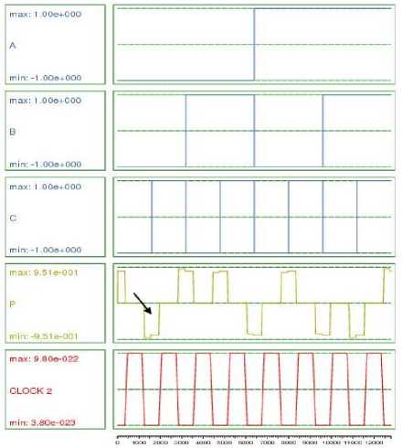
Fig.11. Simulation Result of Parity generator circuit.
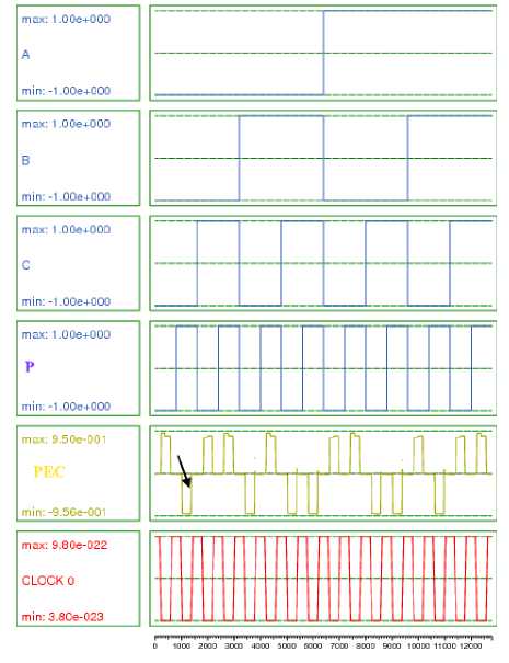
Fig.12. Simulation Result of Parity checker circuit.
-
D. Energy Estimation of Proposed Parity Generator And Checker Circuit
The estimation of energy dissipation is performed at three value of kink energy (0.5Ek, 1Ek and 1.5Ek) at temperature T=2 0K. Also, their thermal layout and power dissipation is very well explained in the sub-section (i) and (ii) .
-
(i) . Energy Dissipation Estimation of Parity Generator
The thermal layout of average energy dissipated in each cell of PG circuit, obtained using QCAPro tool is shown in Fig. 11. Energy Dissipation scale for each cell is in terms of mev. Cells with dark spot show a large amount of power dissipation on an average.
A detailed study of power dissipation is carried out on the basis of kink energy. The results of variation on power dissipation are shown in Table-5. The effect on power dissipation due to kink energy is shown in a graphical manner, Fig. 13. It is seen that maximum, average and average switching energy dissipation is increasing with the increment in kink energy, while the minimum energy and average leakage energy dissipation decrease with the kink energy.
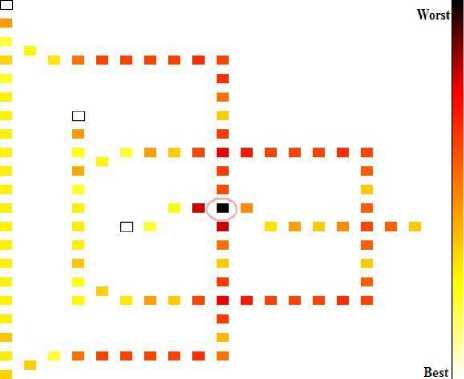
Fig.13. Thermal hotspot map of PG.
Table 5. Energy dissipation of PG for different kink energies
|
Maximum Kink Energy, E k |
|||
|
E k = 0.5mev |
E k = 1mev |
E k = 1.5mev |
|
|
Max Energy Diss |
0.47855 |
0.51347 |
0.56994 |
|
Avg Energy Diss |
0.26148 |
0.33068 |
0.41662 |
|
Min Energy Diss |
0.05541 |
0.15764 |
0.27180 |
|
Avg Leakage Energy Diss |
0.05600 |
0.15892 |
0.27356 |
|
Avg Switching Energy Diss |
0.20548 |
0.17176 |
0.14306 |
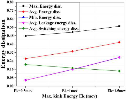
Fig.14. Kink energy vs energy dissipation graph for PG.
-
(ii) . Energy Dissipation Estimation of Parity Checker
The thermal layout of a parity checker, obtained from QCAPro tool is shown in Fig. 15. Only one device cell of the majority is consuming more power, which is encircled by a pink circle. Darker the color of the cell more is the energy consumption of the particular cell. A comprehensive study of power dissipation for the proposed PC circuit is shown in Table 5. A convenient attempt is made to show the effect of kink energy on power dissipation. The same type of relation is funded to be seen between kink energy and power dissipation as it was in the case of parity generator. A graphical representation is displayed in Fig. 16.
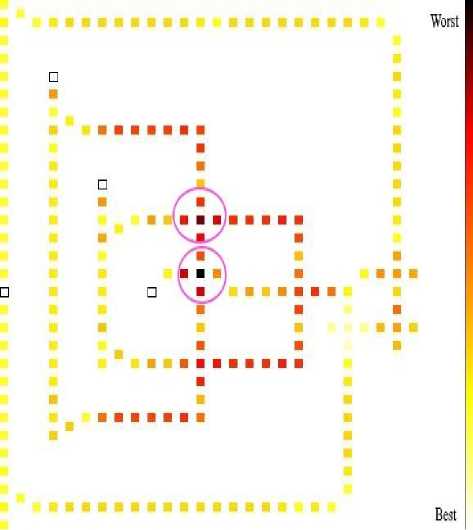
Fig.15. Thermal hotspot map of PC.
Table 6. Energy dissipation of PC for different kink energies
|
Maximum Kink Energy, E k |
|||
|
E k = 0.5mev |
E k = 1mev |
E k = 1.5mev |
|
|
Max Energy Diss |
0.90676 |
0.98953 |
1.11543 |
|
AvgEnergy Diss |
0.41069 |
0.57362 |
0.83347 |
|
Min Energy Diss |
0.11325 |
0.32403 |
0.56040 |
|
Avg Leakage Energy Diss |
0.11402 |
0.32550 |
0.56268 |
|
Avg Switching Energy Diss |
0.29667 |
0.24812 |
0.27079 |
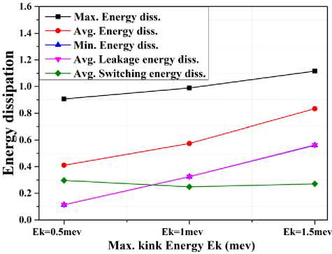
Fig.16. Kink energy vs energy dissipation graph for PC.
-
V. Comparative Analysis Results
In this section, we have presented the comparative analysis results with the existing circuit [20,21,22,23,24]. Table 6 drawn the comparative study of the proposed and existing circuit in terms of clock cycle delay and clock pulse utilize. It is found that proposed circuit has less latency and a minimum number of clock zones, as depicted in Table 7.
Table 7. Comparative study of PG and PC circuits.
|
Delay in PG |
Delay in PC |
Clock pulses used in PG |
Clock pulses used in PC |
|
|
As in [20] |
2 |
N.A. |
12 |
N.A. |
|
As in [21] |
1.5 |
3 |
6 |
8 |
|
As in [22] |
2.5 |
1.5 |
4 |
6 |
|
As in [23] |
2 |
2.25 |
8 |
9 |
|
As in [24] |
2 |
2 |
7 |
8 |
|
Proposed |
0.5 |
1 |
3 |
5 |
|
% Improvement with respect to [20] |
75 |
75 |
||
|
% Improvement with respect to [21] |
66.6 |
66.6 |
50 |
37.5 |
|
% Improvement with respect to [22] |
20 |
33.33 |
25 |
16.66 |
|
% Improvement with respect to [23] |
75 |
55.55 |
62.5 |
44.44 |
|
% Improvement with respect to [24] |
3 |
50 |
57.14 |
37.5 |
-
VI. Conclusion
In this paper, a novel design of even parity generator and checker circuit in QCA framework is presented that reduces the latency as well as clock zones utilize as compared to previously existing designs. Along with the QCA layout, this paper also provides the simulation waveform, thermal layout, and energy dissipation estimation. Circuits are designed using minimum no. of clocks and the projected designs are simulated for three-bit message signal. The output of both the circuits is successfully obtained and verified using QCADesigner tool. The minimum, maximum, average, and switching power dissipation is neatly represented in graphical form. It will help the researchers to understand the relation in a more precise way. Also we secured the precise output values with high kink energy.
Journal of Computer, Electrical, Automation, Control and Information Engineering 8, no. 3, pp. 491-497, 2014.
-
[24] N. R. G, P. C. Srikanth, and P. Sharan, "A novel quantumdot cellular automata for parity bit generator and parity checker," International Journal of Emerging Technology in Computer Science & Electronics , 14, 2015.
References Design of Quantum Dot Cellular Automata Based Parity Generator and Checker with Minimum Clocks and Latency
- C.S. Lent, S., P. Douglas Tougaw, Wolfgang Porod, and Gary H. Bernstein. "Quantum cellular automata." Nanotechnology 4, no. 1 (1993): 49.
- Neeraj Kumar Misra, Subodh Wairya and Vinod Kumar Singh, "Frame of Reversible BCD Adder and Carry Skip BCD Adder and Optimization Using New Reversible Logic Gates for Quantum-Dot Cellular Automata", Australian Journal of Basic and Applied Sciences, vol 9, issue 31, pp. 286-298, 2015.
- Walus, Konrad, Timothy J. Dysart, Graham A. Jullien, and R. AriefBudiman. "QCADesigner: A rapid design and simulation tool for quantum-dot cellular automata." Nanotechnology, IEEE Transactions on 3, no. 1 (2004): 26-31.
- Bibhash Sen, Manojit Dutta, Samik Some, and Biplab K. Sikdar. "Realizing Reversible Computing in QCA Framework Resulting in Efficient Design of Testable ALU." ACM Journal on Emerging Technologies in Computing Systems (JETC), vol. 11, no. 3, page 30, 2014
- International Technology Roadmap for Semiconductors (ITRS), [Online]. Available: http://www.itrs.net
- Snider, Gregory L., Alexei O. Orlov, I. Amlani, X. Zuo, G. H. Bernstein, C. S. Lent, J. L. Merz, and W. Porod. "Quantum-dot cellular automata." Journal of Vacuum Science & Technology A 17, no. 4, pp.1394-1398, 1999.
- Prateek Agrawal, S.R.P. Sinha, and S. Wairya. "Quantum Dot Cellular Automata Based Parity Generator and Detector: A Review." International Journal of Electronics and Communication Engineering, no. 5, 3,(2016), 41-50.
- Neeraj Kumar Misra, Subodh Wairya and Vinod Kumar Singh, "Approach to Design a High Performance fault-Tolerant Reversible ALU", International Journal of Circuit and Architectural design, Inderscience, vol. 2, no. 1, pp. 83-103, 2016.
- Seminario, Jorge M., Pedro A. Derosa, Luis E. Cordova, and Brian H. Bozard. "A molecular device operating at terahertz frequencies: theoretical simulations." IEEE Transactions on Nanotechnology, vol. 3, no. 1,pp. 215-218, 2004
- Neeraj Kumar Misra, Subodh Wairya, Vinod Kumar Singh, "Optimized Approach for Reversible Code Converters Using Quantum-Dot Cellular Automata", In Proceedings of the 4th International Conference on Frontiers in Intelligent Computing: Theory and Applications (FICTA), Springer India, pp.367-378, 2016.
- Lent, Craig S., and Beth Isaksen. "Clocked molecular quantum-dot cellular automata." IEEE Transactions on Electron Devices, 50, no. 9, pp. 1890-1896, 2003.
- Orlov, A. O., G. Toth, I. Amlani, R. Kummamuru, R. Ramasubramaniam, C. S. Lent, G. H. Bernstein, and G. L. Snider. "Experimental studies of clocked quantum-dot cellular automata devices." In Device Research Conference, 2000. Conference Digest. 58th DRC, pp. 157-158, 2000.
- Neeraj Kumar Misra, Subodh Wairya and Vinod Kumar Singh, "Approaches to Design Feasible Error Control Scheme Based on Reversible Series Gates" European Journal of Scientific Research, vol. 129, no. 3, pp. 224-240, 2015.
- Qadir, Fasel, Peer Zahoor Ahmad, Shahi Jahan Wani, and M. A. Peer. "Quantum-Dot Cellular Automata: Theory and Application." In Machine Intelligence and Research Advancement (ICMIRA), 2013 International Conference on, pp. 540-544. IEEE, 2013.
- Gurmohan Singh, R. K. Sarin, and Balwinder Raj. "A novel robust exclusive-OR function implementation in QCA nanotechnology with energy dissipation analysis." Journal of Computational Electronics 15.2, pp. 455-465, 2016
- Chakraborty, Rupak, Debashis De, Ajmal Khan, Chhandak Mukherjee, and Sarah Pramanik. "Effect of temperature and kink energy in multilevel digital circuit using Quantum dot cellular automata." In Computers and Devices for Communication (CODEC), 2012 5th International Conference on, pp. 1-4. IEEE, 2012.
- Saket Srivastava, Arjun Asthana, SanjuktaBhanja, and Sudeep Sarkar. "QCAPro-an error-power estimation tool for QCA circuit design." In Circuits and Systems (ISCAS), 2011 IEEE International Symposium on, pp. 2377-2380. IEEE, 2011.
- Bibhash Sen, Siddhant Ganeriwal, and Biplab K. Sikdar. "Reversible logic-based fault-tolerant nanocircuits in QCA." ISRN Electronics, 2013.
- Saket Srivastava, Sudeep Sarkar, and SanjuktaBhanja. "Estimation of upper bound of power dissipation in QCA circuits." IEEE Transactions on Nanotechnology, vol. 8, no. 1 pp. 116-127, 2008.
- S. Shin, G. Lee, and K. Yoo, "Design of Exclusive-OR Logic Gate on Quantum-Dot Cellular Automata," International Journal of Control and Automation, 8, 95-104, 2015.
- M. Mustafa, and M. R. Beigh, "Design and implementation of quantum cellular automata based novel parity generator and checker circuits with minimum complexity and cell count," Indian Journal of Pure and Applied Physics, 51, pp. 60-66, 2013.
- Firdous Ahmad, Peer Zahoor Ahmad, and G. Mohiud din Bhat. "Design and analysis of odd-and even-parity generators and checkers using Quantum-dot Cellular Automata (QCA)." In Computing for Sustainable Global Development (INDIACom), 2015 2nd International Conference on, pp. 187-194, 2015.
- Santanu Santra, and Utpal Roy. "Design and Optimization of Parity Generator and Parity Checker Based On Quantum-dot Cellular Automata."World Academy of Science, Engineering and Technology, International Journal of Computer, Electrical, Automation, Control and Information Engineering 8, no. 3, pp. 491-497, 2014.
- N. R. G, P. C. Srikanth, and P. Sharan, "A novel quantum-dot cellular automata for parity bit generator and parity checker,"International Journal of Emerging Technology in Computer Science & Electronics, 14, 2015.
