Design, simulation, and fabrication of silicon-on-insulator MEMS vibratory decoupled gyroscope

Author: Verma Payal, Pavelyev Vladimir Sergeevich, Volodkin Boris Olegovich, Tukmakov Konstantin Nickolaevich, Reshetnikov Anton Sergeevich, Andreeva Tatiana Vitalievna, Fomchenkov Sergey Alexandrovich, Khonina Svetlana Nikolaevna
Journal: Компьютерная оптика @computer-optics
Section: Opto-it
Article in issue: 5 т.40, 2016.
Free access
This paper reports the design and fabrication of a 2-degree-of-freedom (DOF) decoupled vibratory gyroscope based on a silicon-on-insulator (SOI) MEMS process. The 2-DOF capacitive comb structure is deliberately designed to have a decoupled drive and sense mode oscillation to prevent the unstable operation due to mechanical coupling, resulting in a low zero rate out-put drift. It is well known that the closer are the drive and sense resonances, the higher is the angular rate resolution of the gyroscope. Generally, this is achieved by using symmetric suspensions, but it results in a reduced bandwidth. The proposed design has been configured to achieve a bandwidth of about 150 Hz, while ensuring the decoupled operation of the drive and sense modes. An analytical method has been employed to study the steady state response of the 2-DOF structure. FEM analysis has been carried out in CoventorWare® MEMS Design software and the simulation results show that the drive resonance occurs at 21.48 kHz and sense resonance at 21.63 kHz, which are in close agreement with the theoretical results. The structure is designed with a 15 µm thick device layer. Fabrication of the design is proposed using a two mask process based on Deep reactive-ion etching (DRIE) and sacrificial wet release etching on a SOI wafer. DRIE etching with an aspect ratio of 1:5 has been successfully carried out as desired and the results have been presented.
Gyroscope, mems, soi process, coventorware®
Short address: https://sciup.org/14059605
IDR: 14059605 | DOI: 10.18287/2412-6179-2016-40-5-664-668-673
Text of the scientific article Design, simulation, and fabrication of silicon-on-insulator MEMS vibratory decoupled gyroscope
Micro-Electro-Mechanical System (MEMS) technology, as one of the most promising technologies in the present technological scenario, has attracted researchers from all parts of the globe and the advancements are taking place at a very fast pace. One of the reasons for the rapid developments in MEMS domain is the adoption of the well-established IC fabrication technology, for the realization of MEMS devices. Among the various MEMS devices, gyroscope is one such device which has vast application areas, few of them being consumer products, automotive, defence, aerospace etc.
MEMS vibratory gyroscope consists of two orthogonal components of accelerometers with a single common proof mass or multiple masses. These gyroscopes are based on the principle of transfer of energy form the drive mode to the sense mode due to Coriolis acceleration, in the event of an angular rate input [1]. With the advancement of MEMS technology, various gyroscope structures were proposed and realized. Based on the application, micro-machined gyroscopes have been broadly divided into three categories: 1) Rate grade gyroscope, 2) Inertial grade gyroscope and 3) Tactical grade gyroscope [1, 2]. Plenty of work has been reported regarding rate grade gyros due to their wide commercial application. The technologies employed in the fabrication of such devices are surface micromachining [3], bulk micromachining [4] and up to some extent electroforming based on Lithogra-phie-Galvanoformung-Abformung (LIGA) process [5, 6].
However, inertial grade and tactical grade gyroscope devices are relatively complex to fabricate, as they are high performance devices required to meet stringent specifications. Other alternate fabrication processes are being employed besides conventional processes in order to meet the stringent technical requirements. The designing of the gyro devices is also of paramount importance in order to render the devices immune to fabrication variations and to avoid extra fabrication trials.
Apart from surface and wet bulk micromachining techniques, micro machining by Deep reactive-ion etching (DRIE) is widely being employed in fabrication of inertial sensors [7, 8]. The Deep reactive-ion etching process has proven to be a versatile process, due to its ability to create complex microstructures in several fields such as technology of computer optics [9 – 11] and others apart from MEMS. One of the main advantages of DRIE process is that high aspect ratio devices can be realized with nearly vertical sidewalls. The advantages of DRIE process are exploited by the use of SOI substrates. SOI substrates have a layer of silicon with a very fine tolerance, separated from the bulk substrate using an oxide layer. The oxide layer is formed by thermal oxidation of the bulk substrate and acts as a dielectric. The presence of the oxide layer provides a very good insulation between the two silicon layers, thereby enhances the electrical performance of the device. The structure is formed in the top silicon layer and hence the thickness of the structural layer is accurately main- tained. Moreover as the device is realized in single crystal silicon, the internal stresses are much less than deposited silicon layers. Further, due to the high selectivity between silicon and silicon-di-oxide in most DRIE machines, the oxide layer also acts as a etch stop which is well defined and controlled, hence reducing process complexity. Several wet and dry release techniques have been reported to release the final structure. Hence the silicon-on-insulator (SOI) process combines the advantages of DRIE and SOI substrate to precisely fabricate complex structures. In this paper we present the fabrication of 2-DOF gyroscope structure with capacitive comb fingers using SOI process.
Gyroscope structure
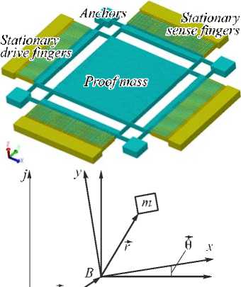
Figure 1 shows the 3D model of the 2-DOF decoupled gyroscope structure. The anchors of the structure are located at the outer boundary of the device and connected to the movable drive and sense electrodes with the help of suspension beams. There are totally 16 beams in the design, 8 beams in the drive direction ( x -direction) and 8 beam in the sense direction ( y -direction). The suspension beams are designed and configured such that the drive and sense mode resonances are decoupled with their resonance frequencies separated to achieve a bandwidth of 150 Hz. This structural configuration exhibits minimum cross coupling effect. The design has two sets of stationary comb fingers, one set for actuation of the proof mass and the other set for sensing the input angular rate. Both the stationary comb finger sets are anchored to the substrate as shown in Fig. 1 a . The device is designed with perforations in the proof mass to aid in sacrificial release of the structure.
a)
b)
-
Fig. 1. (a) Solid model; (b) mass-spring-damper configuration of a 2-DOF vibratory gyroscope [14]
Dynamics and steady state response
A mass-spring-damper configuration shown in Fig. 1b has been considered to derive the dynamic equations of the presented 2-DOF gyroscope device, using vector analysis. The simplified differential equation associated with each degree of freedom can be represented as:
..
mx + cxx + kxx = Fd (t),(1)
my + cy у + kyy = -2mxQz.(2)
The term F d ( t )= F 0sin( ю t ) represents the electrical driving force with which the mass m , is actuated by an amplitude equal to x . The notations k x , k y represent the spring constants and c x , c y represent the damping constants as shown in Fig. 1 b . Q z represents the input angular rate.
In order to analyze frequency response of gyroscope [12– 15], we take the Laplace transforms of Eqs. (1), (2), assuming angular rate, and solve these for corresponding displacements to yield,
X(i ю) = f0Ax (ю)exp{ф x (to)},(3)
Y (i ю) = 2Q zf юAx (ю) Ay (ю)exp {^ y (ю)},(4)
where,
A (ю) = 1/ ю2 + ю2 }2 + 4X 2ю2,(3a)
xxx ф x (ю) = - tan 2Хю,(3b)
Ю x -ю
Ay (ю) = 1/^(ю2 + ю2 )2 + 4X 2 ю2,(4a)
2X ю фу (ю) = —tan , юу -ю
^у (ю) ={ф x (ю) +ф У (ю)} , ю x = kx / m; ю2 = ky /m; fo = Fo / m,
Xx = cx /2 m ; Xx = c ,/2 m . xx yy
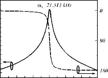
Fig. 2 shows the variations of drive amplitude and phase with frequency. The amplitude has been calculated by making use of magnitude of Eq. (3) considering ambient damping as a parameter. The plot shows one resonance frequency, ю x , where amplitude is the maximum. The results of phase associated to drive amplitude as illustrated in this figure has been evaluated by using Eq. (2b). The phase values at these discontinuity points lead to 90o.
Amplilude, |x№)>|, dBm Phase, фл(со), deg
-125
-BO
-135
-140
-145
-150
-155
-160
-165
20 21 22 23
Frequency, kHz
-
Fig. 2. Drive amplitude and phase spectral responses
Fig. 3 relate to the sense mass amplitude and emerged phase variations with frequency. Fig. 3 has been calculat- ed with the help of sense mode amplitude expression (4). This figure shows two resonances at which amplitude peaks. The second peak belongs to sense resonance frequency, ωy, which is the sense point of the device. First peak has occurred due to transfer of drive amplitude as a consequence of Coriolis. This has been plotted by making use of Eq. (4c).
a)
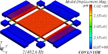
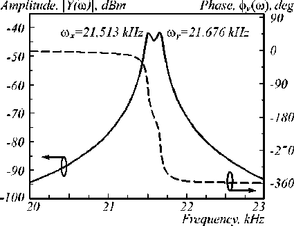
Fig. 3 Sense amplitude and phase spectral responses
b)
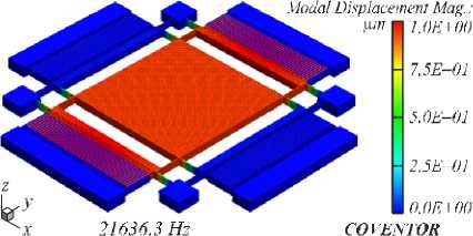
Fig. 4. FEA: Mode shape simulation of a 1-DOF drive mode and 1-DOF sense mode gyroscope
SOI fabrication process
Optimization and FEM simulation result
The design is optimized for compatibility with DRIE and sacrificial wet release process.
The thickness of the silicon device layer is chosen to be 15 µm as the key structural layer and the gap between comb fingers is maintained at 3 microns. The combination of this thickness and comb finger gap yields a considerably high base capacitance of about 2 pF. The proof mass is provided with perforations of size 8 × 8 micron to aid in buried oxide etching. The spring dimensions have been optimized to achieve decoupled drive and sense mode oscillations. The optimum design parameters are listed in Table 1.
Table 1. Parameter values used for calculations
|
Parameters |
Values |
|
m |
7.776 × 10⁻⁸ kg |
|
Spring constant ( k x ) |
1.420 × 10³N/m |
|
Spring constant ( k y ) |
1.442 × 10³N/m |
|
Drive frequency ( ω x ) |
21.513 kHz |
|
Sense frequency ( ω y ) |
21.676 kHz |
|
Bandwidth |
163 Hz |
|
Beam width |
8 µm |
|
Base capacitance |
2 pF |
|
Perforation size |
8 µm |
|
Young’s Modulus |
185 GPa |
In order to verify the above design parameters extracted from the analytical model, the device is modeled and simulated in CoventorWare® MEMS design environment [16, 17]. Modal analysis is carried out to obtain the resonance frequencies and mode shapes of the device as shown in Fig. 4. The drive and sense resonance frequencies of the device are located at about 21.48 kHz (Fig. 4 a ) and 21.63 kHz (Fig. 4 b ). This is in close agreement with the theoretical values of 21.513 kHz and 21.676 kHz for the drive and sense modes respectively.
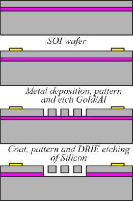
The proposed fabrication process uses silicon-on-insulator wafer with 15 µm device layer, 4 µm buried oxide and 675 µm handle layer as the starting material (Fig. 5).
Sacrificed Etch o f Burned Oxide.
Fig. 5. Fabrication steps of SOI MEMS gyroscope
The process is based on Deep reactive Ion etching to realize high aspect ratio structure and finally the structure is released by sacrificial etching of the buried oxide using Vapor phase etching. The process begins with the deposition of Cr/Au to a thickness of 200Å / 2000Å on the silicon device layer using sputtering process. Subsequently, lithography and etching is carried out selectively to realize the metal pads for wire bonding. The pads are located on the four proof mass anchors and on all the four stationary comb anchors. This is followed by Lithography of the structural layer and subsequently baking is done to harden the resist before it undergoes DRIE process. Next, silicon is etched up to buried oxide using controlled process parameters. At the end of this step, the structural layer is formed with the necessary metal pads. The structural layer is then released by sacrificial etching of buried oxide using Vapor phase etching process. The etching is time based and ensures perfect release of the structure while limiting the undercut to a minimum.
Fabrication results
As per the process flow described above, the device is fabricated using the two mask SOI process. Lithography process has been carried out to pattern the structure with a minimum feature size of 3 µm that is the gap between comb fingers. Microscope image of the device after lithography patterning is shown in Fig. 6.
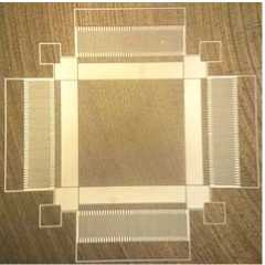
Fig. 6. Photolithography pattern of the device
After completion of photolithography (Fig. 6), the structure is etched using Deep reactive ion etching process on the “Etna 100 PT" (HT MTD, Russia) equipment, based on the Bosch process. The Bosch-process is an inductively coupled configuration, uses a two step plasma process, which alternates between etching (SF 6 / Ar) and passivation step (C 4 F 8 / Ar). An important requirement, allowing to achieve the desired depth of etching structure is the need to preserve the masking layer during the entire etching step. To do this during the process cooling takes periodically a substrate that can be carried out using the following steps:
-
1. Feed helium to the underside of the substrate. The helium pressure on the substrate is about 0.012 mbar.
-
2. Carrying-Bosh process interruptions 3 times in 50 cycles for etching silicon structure 15 m in height. Every 50 cycles do not last more than 10 minutes. Silicon etching depth in one cycle is 100 nm.
Reducing the etch rate achieved by adding an argon during the etching step, which substantially reduces the roughness of the walls. The pressure in the installation of approximately 0.1 mbar. In order pumping turbo molecular pump is used, which enables the atmosphere in the reactor be updated fast enough. Flow SF 6 /Ar of about 40/60 cm3/min, and the flow C 4 F 8 /Ar about 90 / 80 cm3/ min. ICP source inductor has a capacity of about 200 watts, and the accelerating power source, who worked exclusively in the etching step in the mode of regulation of the self-bias potential of the substrate (constant DC-Bias), is 60 V, does not exceed 10 watts.
At the end of etching silicon substrate cleaning is performed in the presence of SF 6 using isotropic etching mode.
The microscope image after DRIE is shown in Fig. 7a-c, showing the comb fingers and perforations in proof mass. Nearly vertical sidewalls are achieved, with an angle 91.2 degree as shown in (Fig. 7c), which is much smaller than the maximum angle of inclination of the walls calculated above.
a)
b)
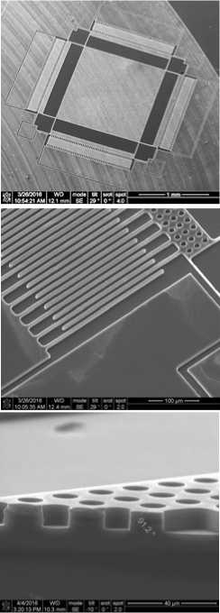
Fig. 7. Etching results
c)
The device layer including the proof mass, movable and stationary comb fingers is etched using DRIE with an aspect ratio of 1 : 5.
Conclusion
This paper presented the design, simulation and fabrication of a 2-DOF capacitive MEMS vibratory gyroscope based on SOI MEMS. The device is designed to achieve decoupled drive and sense resonance modes and for SOI process compatibility. Analytical and simulation results of resonance frequency analysis are in good agreement. The advantages of the DRIE process have been coupled with the benefits of SOI wafer to realize the capacitive structure with a 2-mask process. Front side release of the structure using wet chemical etching is proposed to avoid the process complexities of releasing the device by bulk etching using DRIE release process. The successful completion of lithography and DRIE which are two major steps of SOI process demonstrates the feasibility of realizing the 2-DOF gyroscope devices using the proposed SOI process.
References Design, simulation, and fabrication of silicon-on-insulator MEMS vibratory decoupled gyroscope
- Yazdi, N. Micromachined nertial sensors/N. Yazdi, F. Ayazi, K. Najafi//Proceedings of the IEEE. -1998. -Vol. 86(8). -P. 1640-1659.
- Alper, S.E. MEMS gyroscopes for tactical-grade inertial measurement applications/S.E. Alper. -PhD dissertation. -Turkey: Middle East Technical University, 2005.
- Oh, Y. A surface-micromachined tunable vibratory gyroscope/Y. Oh, B. Lee, S. Baek, H. Kim, J. Kim, S. Kang, C. Song//Proceedings of the IEEE, Micro Electro Mechanical Systems, MEMS '97, Tenth Annual International Workshop 1997. -1997. -P. 272-277. - DOI: 10.1109/MEMSYS.1997.581824
- Kovacs, G.T.A. Bulk micromachining of silicon/G.T.A. Kovacs, N.I. Maluf, K.E. Petersen//Proceedings of the IEEE. -1998. -Vol. 86(8). -P. 1536-1551.
- Verma, P. New design architecture of a 3-DOF vibratory gyroscope with robust drive operation mode and implementation/P. Verma, C. Shekhar, S.K. Arya, R. Gopal//Microsystem Technologies. -2015. -Vol. 21(10). -P. 2175-2185. -DOI: 10.1007/s00542-014-2384-4.
- Verma, P. Ultraviolet-LIGA based fabrication and characterization of a non-resonant drive mode vibratory gyro/accelerometer/P. Verma, K.Z. Khan, S.N. Khonina, N.L. Kazanskiy, R. Gopal//Journal of Micro/Nanolithography, MEMS, and MOEMS. -2016. -Vol. 15(3). -035001. -DOI: 10.1117/1.JMM.15.3.035001.
- Ishihara, K. An inertial sensor technology using DRIE and wafer Bonding with interconnecting capability/K. Ishihara, C.F. Yung, A.A. Ayon, M.A. Schmidt//Journal of Microelectromechanical Systems. -1999. -Vol. 8(4). -P. 403-408. - DOI: 10.1109/84.809054
- Li, Z. A bulk micromachined vibratory lateral gyroscope fabricated with wafer bonding and deep trench etching/Z. Li, Z. Yang, Z. Xiao, Y. Hao, T. Li, G. Wu, Y. Wang//Sensors and Actuators A: Physical. -2000. -Vol. 83(1-3). -P. 24-29. - DOI: 10.1016/S0924-4247(99)00375-1
- Kazanskiy, N.L. Microprofile formation by thermal oxidation of molybdenum films/N.L. Kazanskiy, O.Yu. Moiseev, S.D. Poletayev//Technical Physics Letters. -2016. -Vol. 42(2). -P. 164-166. - DOI: 10.1134/S1063785016020085
- Kazanskiy, N.L. Formation of images using multilevel diffractive lens/N.L. Kazanskiy, S.N. Khonina, R.V. Skidanov, A.A. Morozov, S.I. Kharitonov, S.G. Volotovskiy//Computer Optics. -2014. -Vol. 38(3). -P. 425-434.
- Volkov, A.V. A method for the diffractive microrelief formationusing the layered photoresist growth/A.V. Volkov, N.L. Kazanskiy, O.Yu. Moiseev, V.A. Soifer//Optics and lasers in Engineering. -1998. -Vol. 29(4-5). -P. 281-288. - DOI: 10.1016/S0143-8166(97)00116-4
- Verma, P. Analytical modeling and simulation of a 2-DOF drive and 1-DOF sense gyro-accelerometer/P. Verma, R. Gopal, S.K. Arya//Microsystem Technologies. -2013. -Vol. 19(8). -P. 1239-1248. -DOI: 10.1007/s00542-012-1725-4.
- Verma, P. Lumped parameter analytic modeling and behavioral simulation of a 3-DOF MEMS gyro-accelerometer/P. Verma, R. Gopal, S.K. Arya//Acta Mechanica Sinica. -2015. -Vol. 31(6). -P. 910-919. - DOI: 10.1007/s10409-015-0512-8
- Verma, P. Dynamic characteristics of vibratory gyro-accelerometer/P. Verma, R. Gopal, S.K. Arya//In: Proceeding of the IEEE, 5th International Conference on Computers and Devices for Communication, University of Calcutta, India, 2012. - DOI: 10.1109/CODEC.2012.6509277
- Verma, P. Parametric sensitivity analysis of a 2-DOF drive and 1-DOF sense modes MEMS gyro-accelerometer structure/P. Verma, P. Agrawal, R. Gopal, S.K. Arya//Advance Science Letters. -2014. -Vol. 20. -P. 1495-1498. - DOI: 10.1166/asl.2014.5557
- Design and fabrication of a 1-DOF drive mode and 2-DOF sense mode micro-gyroscope using SU-8 based UV-LIGA process/P. Verma, S. Juneja, D.A. Savelyev, S.N. Khonina, R. Gopal//In: Proceedings of the AIP. -2016. -Vol. 1724(1). - DOI: 10.1063/1.4945137
- Design and simulation of non-resonant 1-DOF drive mode and anchored 2-DOF sense mode gyroscope for implementation using UV-LIGA process/P. Verma, R. Gopal, M.A. Butt, S.V. Khonina, R.V. Skidanov//In: Proceedings of SPIE. -2016. -Vol. 9807. -98070D. - DOI: 10.1117/12.2231372
