Designing a Novel Ternary Multiplier Using CNTFET

Author: Nooshin Azimi, Hamidreza Hoseini, Abbas Shahsavari
Journal: International Journal of Modern Education and Computer Science (IJMECS) @ijmecs
Article in issue: 11 vol.6, 2014.
Free access
Today, multipliers are included as substantial keys of many systems with high efficiency such as FIR filters, microprocessors and processors of digital signals. The efficiency of the systems are mainly evaluated by their multipliers capability since multipliers are generally the slowest components of a system while occupying the most space. Multiple Valued Logic reduces the number of the required operations to implement a function and decreases the chip surface. Carbon Nanotube Field Effect Transistors (CNTFET) are considered as good substitutes for Silicon Transistors (MOSFET). Combining the abilities of Carbon Nanotubes Transistors with the advantages of Multiple Valued can provide a unique design which has a higher speed and less complexity. In this paper, a new multiplier is presented by nanotechnology using a ternary logic that improves the consuming power, raises the speed and decreased the chip surface as well. The presented design is simulated using CNTFET of Stanford University and HSPICE software, and the results are compared with other instances.
CNTFET, Multi-valued logic (MVL), Multiplier, ternary logic, carbon nanotube
Short address: https://sciup.org/15014705
IDR: 15014705
Text of the scientific article Designing a Novel Ternary Multiplier Using CNTFET
Published Online November 2014 in MECS DOI: 10.5815/ijmecs.2014.11.06
Speed improvement of computers is a major goal for specialists to study and research on this field, and the result is progressing the technology of VLSI as more dimensional reduction and more complexity of the chips.
Multipliers are regarded as the most important factors in designing of digital systems. The speed of the systems is often evaluated by the speed of the system multiplier. Although multiplying implementation requires a complex hardware which occupies much space, it is the slowest component of a system computation. Thus, achieving the high speed, the low cost and the reduction of chip surface are the main criteria to design a multiplier.
The most considerable obstacles of increasing the speed and decreasing the size due to the circuit RC delays are circuit interconnections so that in modern designs, more than half of the occupied space is for circuit interconnections. Herein, Multi Valued Logic will potentially have the ability of reducing the number of the connections and active elements as well. In addition, the range of data transmission of each wire is increased significantly by using Multi Valued Logicso that it raises the circuit efficiency of the chip size and speed [1], [2].
In recent years, Carbon Nanotubes (CNT) are highly regarded for their unique features. Using Carbon Nanotubes to implement circuits provides the possibility of utilizing the benefits of Multi Valued Logic.
The general structure of this paper is as follows: Multi Valued Logic is described in section 2. In section 3, Carbon Nanotubes Field Effect is described. The proposed Multi Valued Multiplier is presented in section 4. The results of the circuit simulation and comparison are presented in section 5. And finally, conclusion is in section 6 of the paper.
-
II. A Review On Multiple Valued Logic
Introducing transistors in 20th century has caused a revolution in the field of Complex Circuits (very large scale integrated systems) [3]. More complexity of computing circuits increased the number of available transistors in chips and it made difficulties such as raised chip surface and produced heat. Circuit interconnections in complex designs of the binary complex circuits occupy more than 75 percent of the chip space [4].
Using circuits with more than two logic surface namely Multi Valued Logic (MVL) is one of the presented methods. It has various benefits compared to Binary Digital Systems.
Multi Valued Logic reduces the number of required operations to implement a special mathematical function and reduces the circuit surface as well. Implementation effectively reduces chip area, number of transistors and consuming power by using Multi Valued Logic compared to the counterpart binary circuits [5], [6], [7].
The chip area in VLSI is indicated by the connections. The number of the connections could be decreased in terms of 1/ (log 2 k) 2 comparing with Binary Logic in K Valued Logic.
The general area of inner connections is specified by their length. Since the length of the connections is indicated by the connections complex, it's obvious that using Multi Valued Logic (MVL) is very useful for implementing massive VLSI circuits.
Connections delay is an important problem in VSLI too. Resistance and capacitor store of the connection sites and inner connection lines make some functional limitations with smaller criteria. If the resistance and capacitor per length are R and S, respectively and L shows the length of the connections, the connections delay (t) is shown by equation (1):
t = RCL2 (1)
If the capacity of the capacitor (C) is with no delay, the resistance (R) per length will be a factor which is increased S times by numeral scale factor. So, the reduction of length (L) is very significant in VLSI connections.
MVL reduces the connections complexity. So the connections length and delay will be decreased so much. Consuming power is also a main important matter in VLSI. Dynamic consuming power is recognized by inner connections capacitors. Therefore, MVL is suitable for the consuming power.
Cross talk is another important issue in VSLI since the space between connections is much decreased. The best solution is to make more space. This is possible when the inner connections density is reduced by multi valued logic. In this paper, Ternary Logic is used to present the multiplier due to the optimum functions of Multi Valued Logic.
-
III. Carbon Nanotube Field Effect Transistor
The evaluations show that using Carbon Nanotube Technology in designing logical circuits and especially in multi valued (multi surface) circuits is led to the reduction of common complexities in designing such circuits and their highlight increase in efficiency. On the other hand, it removes the present limitations in Silicon Transistors.
Moore in 1965 predicted that the number of transistors on a chip would be duplicated every two years [8]. But the reduction of transistors dimensions in CMOS technology due to limitations such as consuming power, reliability, production cost growth and the transistors size will be ended very soon.
Carbon Nanotube Transistors are good substitutes for complex circuits based on Silicon Transistors. Carbon Nanotubes (CNT) made of carbon plates with one atom diameter and as an empty cylinder were detected in 1991 by Ijima from NEC Company [9].
Nanotubes can be formed as Multi Walled Carbon Nanotubes (MWCNT) or Single Walled Carbon Nanotubes (SWCNT) [10]. SWCNTs are made of one cylinder while MWCNTs have more than one cylinder. In term of the way their graphic plate maker is rolled, Nanotubes are formed as conductive or semi-conductive. Figure 1 shows the structure of MWCNTs and SWCNTs [11].
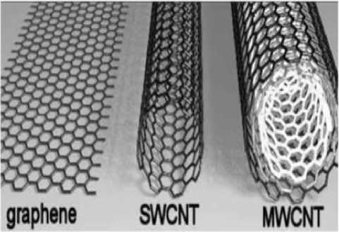
Fig.1. The Structure of Carbon Nanotube Transistors
The transistors based on Carbon Nanotubes or CNTFETs were introduced as the ideal substitutes for Silicon Transistors due to their unique features such as very small sizes, high speed, very low consuming power, and their similar function to MOSFETs [12].
The operational basis of CNTFETs is same as Silicon transistors containing a semi-conductive nanotube (which acts as a guiding channel) and a connection bridge of Drain and Source. The transistor is electrostatically ON and OFF through a gate. There are three different kinds of CNTFETs. The first group is called Schottky Barrier (SB) transistors. SB–CNTFET conductivity is controlled based on a direct tunneling as a Schottky Barrier on Source and Channel connection [13]. The second form is CNTFETs like MOSFETs transistors. These transistors have unipolar behaviors and have a higher comparability comparing with SB–CNTFETs. They also have a very higher current due to the lack of Schottky Barrier in ON mode [14], [15]. The third group is band-to-band tunneling CNTFET. These Transistors have super cut-off characteristics and low ON currents. They are very appropriate for ultra-low power and sub-threshold circuit designing [16], [17].
Figure 2 shows the structure and kinds of the transistors based on Carbon Nanotubes.
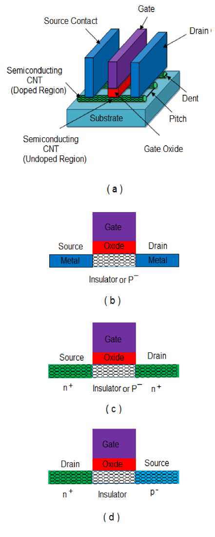
Fig. 2. (a) Transistor Structure Based on CNTFET (b) SB – CNTFET (c) MOSFET-like CNTFET (d) T – CNTFET
-
IV. The Proposed MVL Multiplier
As it's mentioned, multiplying is one of time consuming operations in processors. And the slowness reason is related to the high number small created multipliers, and then adding them to get the ultimate product. Using Multi Valued Logic leads to increasing data transmission speed and as a result achieving the high speed. Yet Ternary Adders have a great number of transistors that using them in the multiplier structure causes the circuit size increase.
The presented design uses an analog multiplier to perform a multiply for a simultaneous achievement to a high speed and circuit size decrease [18]. This multiplier inlet is processed by a transformer of ternary to analog. Finally, the created product is turned into analog by an analog multiplier which remarkably reduces the number of the consuming transistors and circuit size.
Simulations use of the benefits of Multi Valued Logic and Carbon Nanotubes in the proposed design improves the consuming power, increases the speed and decreases the chip size as well.
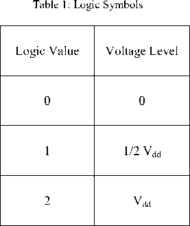
The input values are presented by different voltage levels. Table 1 shows the values.
According to the above advantages, MOSFET –like CNTFETs and their operational similarity with MOSFETs, these transistors are used in this paper.
-
A. Ternary to analog converter using Carbon Nanotubes
The proposed circuit is ternary converter that makes nine different output levels for the inputs 0, 1, 2. The input values are presented by different voltage levels. Figure 3 shows the proposed converter circuit in transistor level.
-
B. Analog to ternary converter using Carbon Nanotubes
The converter turns the produced product by the analog multiplier into the ternary.
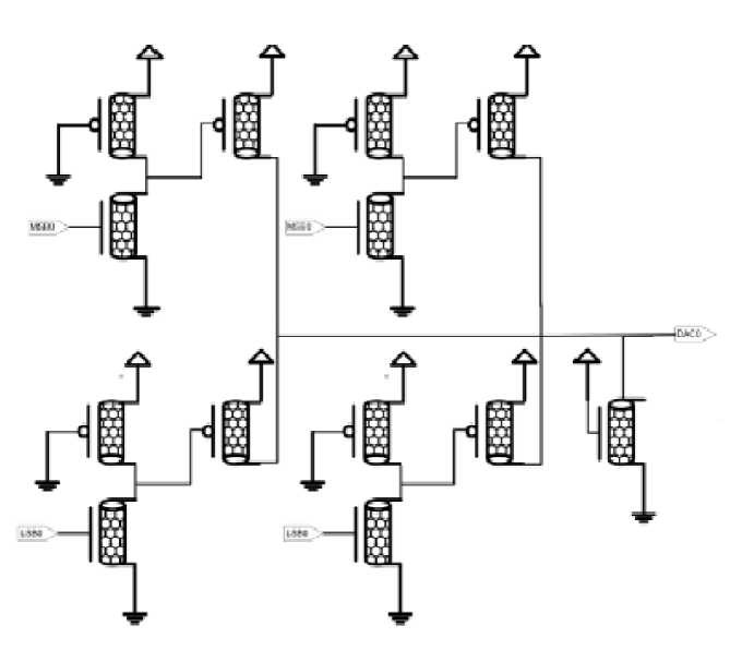
Fig.3. Ternary to analog converter by Carbon Nanotubes
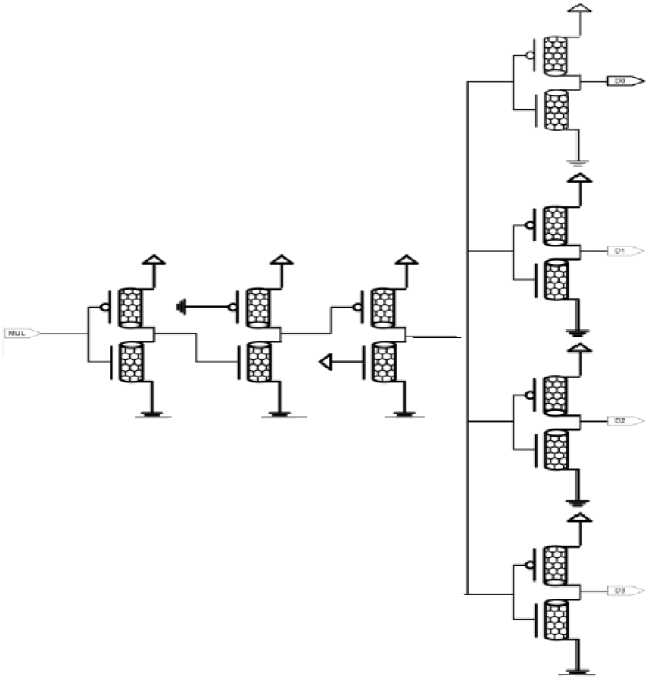
Fig.4. Analog to ternary to analog converter by Carbon Nanotubes
-
C. The proposed design of a Ternary Multiplier by Carbon Nanotubes
The given design uses the multiplier [18] as a multiplier core. Two converter of ternary to analog are placed on the multiplier input.
The attained results are multiplied as analog on the multiplier output, and are turned into a ternary by a converter.
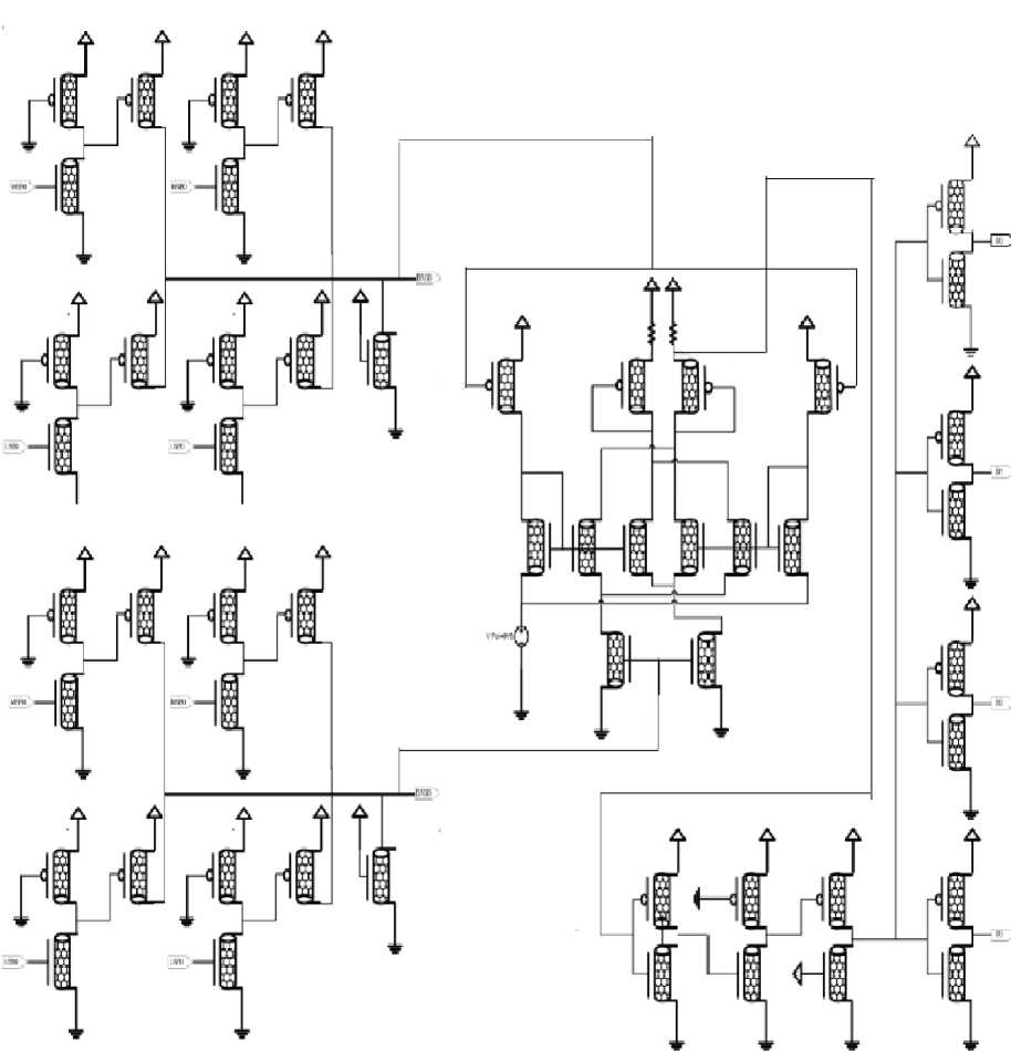
Fig.5. The Proposed Design of a Ternary Multiplier by Carbon Nanotubes
-
V. The Comparison Results
The proposed multiplier is compared with present ternary multipliers considering the number of the transistors and other parameters in tables 2 and3.
Table 2: The Comparison between the Number of the Proposed Multiplier Transistors and the Present Ternary Multipliers
|
Multiplier |
[21] |
[20] |
[19] |
Proposed Multiplier |
|
the Number of Transistors |
650 |
210 |
120 |
52 |
Table 3: The Comparison between the Proposed Multiplier Parameters and Two Bit Binary Multiplier
|
Multiplier |
Power consumption |
Delay |
|
[22] |
4.1667e -3 |
2.6e -7 |
|
Proposed Multiplier |
5.8106e -2 |
6.6874e -8 |
As it's given in the above table, the proposed multiplier is remarkably decreased considering the number of transistors compared to the present multipliers, and this leads to the reduction of circuit complexity and chip size.
-
VI. Conclusion
This paper has presented the designing of a new ternary multiplier based on carbon nanotube field effect transistors (CNTFETs).
As previously noted, optimizing the circuit speed and area is a major design issue. However, area and speed are usually conflicting constraints (parameters or factors), so for the most part, the improvement of speed results in larger areas.
There are two converters and one analog multiplier used in the process of designing the presented two bit ternary multiplier in this paper. Using the converter has notable advantages in designing process such as reducing the number of transistors and circuit size. Other profits of this multiplier circuit are its simplicity and higher speed compared to binary and ternary digital multipliers.
All simulations were performed in HSPICE by using the CNTFET model provided by [23]. Simulation results have confirmed the simplicity, and delay improvements is possible by the proposed ternary converter at transistor levels. The presented results show that the design approach using the ternary converter combined with analog multiplier is a practical solution for low complexity and high speed VLSI design with CNTFETs in nanoscale era.
References Designing a Novel Ternary Multiplier Using CNTFET
- E. V. Dubova, "Multiple-valued logic in VLSI: challenges and opportunities", Proceedings of Conference NORCHIP'99, 1999, pp.340-350. Doi:10.1.100.1809.
- E. V. Dubrova, "Multiple -Valued Logic in VLSI Design", International Journal on Multiple -Valued Logic, 2002.
- Peiman Keshavarzian and Keivan Navi,"Universal ternary logic circuit design through carbon nanotube technology"Electrical and Computer Engineering Department, Nanoelectronics and Quantum Computing Laboratory of Shahid Beheshti University , 2009. doi:10.1504/IJNT.2009.027557.
- Gravati M, Valle M, "Modelling mismatch effects in CMOS translinear loops and current mode multipliers", In Proc European Conference on Circuit Theory and Design (ECCTD'05), Cork (Ireland),Aug 29 - Sept 1, Vol. III, pp.373-376,2005. doi:10.1109/ECCTD.2005.1523138.
- M. Mukaidono .Regular ternary logic functions - ternary logic functions suitable for treating ambiguity. IEEE Trans. Computers .1986; C-35(2):179 - 183.
- Jain, A. K., R. J. Bolton and M. H. Abd-El-Barr, "CMOS Multiple-valued Logic Design, Part I: Circuit Implementation", IEEE Transactions on Circuits and Systems-Fundamental Theory and Applications, Vol. 40, No. 8, pp. 503-514, 1993.
- Kameyama, M., "Toward the Age of Beyond-Binary Electronics and Systems", Proceedings of 20th IEEE International Symposium on Multiple-Valued Logic, pp. 162-166, 1990.
- G. E. Moore, "Cramming more components into integrated circuits," Electronics, vol. 38, 1965.
- S. Ijiima, Nature, 354, 56 (1991). http://dx.doi.org/10.1038/354056a0.
- P. L. McEuen, M. Fuhrer and H. Park, IEEE T. Nan-otechn. 1, 78 (2002).
- Peiman Keshavarzian and Keivan Navi,"Universal ternary logic circuit design through carbon nanotube technology"Electrical and Computer Engineering Department, Nanoelectronics and Quantum Computing Laboratory of Shahid Beheshti University , 2009. doi:10.1504/IJNT.2009.027557.
- Raychowdhury A, Roy K, "A Novel Multiple-Valued Logic Design Using Ballistic Carbon Nanotube FETs", ISMVL, Proceedings of the 34th International Symposium on Multiple-Valued Logic, pp. 14-19, 2004.
- S. Heinze, J. Tersoff, R. Martel, V. Derycke, J. Appenzeller, and P. Avouris, "Carbon Nanotubes as Schottky Barrier Transistors," Phys. Rev. Lett., vol. 89, no. 10, pp. 1068011-1068014, 2002.
- A. Javey, R. Tu, D. B. Farmer, J. Guo, R. G. Gordon, and H. Dai, "High Performance n-Type Carbon Nanotube Field-Effect Transistors with Chemically Doped Contacts," Nano Lett., vol. 5, no. 2, pp. 345-348, 2005.
- Deng J, Wong H.S, "A Compact Model for Carbon Nanotube field-Effect Transistors Including Nonidealities and its Application- Part II: Full Device Model and Circuit Performance Benchmarking," IEEE Trans. Electron Devices, vol. 54, no. 12, pp. 3195-3205, Dec. 2007.
- A. Raychowdhury and K. Roy, IEEE T. Circuits Syst.54, 2391(2007). http://dx.doi.org/10.1109/TCSI. 2007.907799.
- A. Javey, R. Tu, D. B. Farmer, J. Guo, R. G. Gordon and H. Dai, Nanoletter 5, 345 (2005).
- Maurizio Valle and Francesco Diotalevi," An analog CMOS four quadrant current-mode multiplier for low power artificial neural network simplementation", Department of Biophysical and Electronic Engineering (DIBE), University of Geneva, 2001.
- Rasmita Sahoo and R. R. Mishra ,Physics group, Birla Institute of Technology and Science, Pilani, Rajasthan, India "Simulations of Carbon Nanotube Field Effect Transistors", International Journal of Electronic Engineering Research ,2009.
- Temel, T.; Morgul, A.; Dept. Of Electr. & Electron. Eng,Bogazici Univ., Istanbul "Implementation of Multi-Valued Logic Gates Using Full Current-Mode CMOS Circuits", 2004.
- A.P. Dhande et. Al,"Design and Implementation of 2 Bit Ternary ALU Slice", 3rd International Conference, Sciences of Electronic (SETIT), IEEE Transc., pp.1-11, 2005.
- A. Bachtold, P. Hadley, T. Nakanishi, and C. Dekker, "Logic circuits with carbon nanotube transistors," Science, vol. 294, no. 5545, pp. 1317–1320, Nov. 2001.
- Stanford University CNFET Model website [Online 2008].Available:http://nano.stanford.edu/model.php?id=23.
