Designing Counter Using Inherent Capability of Quantum-dot Cellular Automata Loops

Author: Soheil Sarmadi, Saeid Azimi, Shadi Sheikhfaal, Shaahin Angizi
Journal: International Journal of Modern Education and Computer Science (IJMECS) @ijmecs
Article in issue: 9 vol.7, 2015.
Free access
Quantum-dot cellular automata presents a promising Nano-scale technology for replacement of conventional CMOS-based circuits. According to the significant role of counters in computing units, designing diverse types of counter circuits has attracted many attentions, so far. This paper presents a QCA-compatible single layer architecture for 4-bit counter circuit, however by generalizing the main idea, n-bit counter can be engendered in a similar way. The proposed circuit is designed without employing conventional flip-flops' structures by allotting the distinct clock cycles to each counting unit. The comparison results with the best-reported structure reveal the superiority of our design in terms of circuit complexity and required layers for accessing to input and output cells. The proper output waveforms obtained by the QCADesigner tool proves the precise functionality of the proposed counter.
Nanoelectronics, Quantum-dot Cellular Automata, Counter Design, QCA loop
Short address: https://sciup.org/15014791
IDR: 15014791
Text of the scientific article Designing Counter Using Inherent Capability of Quantum-dot Cellular Automata Loops
Published Online September 2015 in MECS
Quantum-dot Cellular Automata (QCA) is introduced in order to be an alternative for conventional CMOS technology. Ongoing shrinkage in CMOS circuits’ dimensions has produced some vital issues such as leakage currents and high power consumption and eventually made them ineffective at Nano-scale architectures [1]. Not only QCA’s advent gives a solution for Nano-scale designing problems, but also its innovative and simple method for illustration of binary logics has attracted lots of attentions. Unlike the transistor-based technologies, QCA can operate based on Columbic Interaction instead of current [2]. The basic unit in QCA is a cell composed of four dots and two excess electrons which lead to two stable states as the first concept of a digital system [3, 4].
Since the introduction of QCA, many studies have been performed to design various logical circuits based on this technology. For instance; declaring the design rules for robust QCA circuits [3], implementing fulladder cell [10,15], design of new Nano-scale devices such as five-input majority gate [6], designs for memory cells [5-8], power dissipation analysis [11] and also array divider designs [16] have been presented.
Much attentions are also paid to practical QCA implementations. A QCA cell can be implemented via four techniques (Metal-island, Molecular, semiconductor, and Magnetic) as is presented in [12]. An accurate operation in QCA circuits could be done in a temperature below 7 Kelvin which is necessary to distinguish between states in a QCA cell. However, many investigations have been made regards to the chance of increasing QCA circuit temperature [13]. These attempts showed that physical characteristics could be changed in order to implement QCA circuits with ability to work in different temperatures.
As is clear, the registers and counters are among the most significant widely used sequential circuits. Counters have a wide area of use which two of the most important ones are dividing frequency and counting pulse. Hence, many efforts for designing efficient counters are made by researchers with focusing on the implementation based on the conventional scheme used in digital designs [5]. However, the authors in [8] have introduced an innovative QCA-compatible design for counters using the inherent capability of QCA loop.
In this paper, with a deep look on the proposed implementation scheme in [8], a single layer and minimized structure for a 4-bit counter circuit is proposed.
The rest of this paper is organized as follow: section II provides a review on QCA basic concepts required for designing circuits. In section III, state-of-the-art designs for QCA counters are addressed. Our proposed design is introduced in Section IV. The simulation and comparison results are prepared in Section V. Two last sections (VI and VII) are also allocated to the conclusion and future works.
-
II. Q ca B ackground
This section is allocated to QCA preliminaries such as wire, inverter and majority gate in addition to QCA clocking mechanism. As is mentioned earlier, the fundamental unit in QCA area is a cell which is composed of four dots on the corners of a square shaped cell, plus two injected electrons. These electrons can be situated in any of the dots. As a result, sixteen different states can be gained for four sites and two electrons of opposite spins [2, 17]. After several displacement through tunnels among dots, two stable states would be gained which are named cell polarization. As is illustrated in Fig. 1(a), one of them is polarized to -1 which is equal to binary “0” and the other one is polarized +1 as the binary “1” [3]. By employing these two stable cells, all QCA elements and gates can be constructed. Fig. 1(b) shows a QCA wire which is constructed via placing several cells next to each other in a line. As a result, the input signal will be propagated cell to cell based on Columbic interaction.
A simple QCA inverter can be implemented using only two cells in a diagonal arrangement as is illustrated in Fig. 2. The input signal is injected to the gate from the left cell and the inverted input signal is propagated from the right cell [3].
One of the principal building blocks in QCA is a majority gate which is configurable for implementing different gates and circuits. As is shown in Fig. 3, a three-input majority voter is constructed of three input cells and one device cell. The main majority calculation based on the following equation (1) is performed in this cell. Another cell is applied as the output cell to propagate the majority polarization [2, 3].
M (A, B, C) = AB + AC + BC (1)
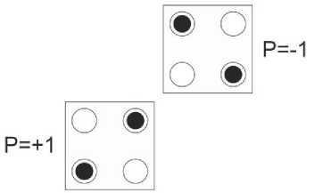
Fig.2. QCA Inverter
As is mentioned earlier this gate is configurable and other gates can be constructed by configuring this gate. For instance, by setting one of the input cells to a constant value, two-input AND or OR gate would be achieved. By forcing one of the cells to polarization -1 (Binary “0”), the produced gate propagates a signal similar to two-input AND gate, as follows:
M (A, B, 0) = AB + (A)(0) + (B)(0) = AB (2)
Similarly, by forcing one of the input cells to polarization +1 (Binary “1”), two-input OR gate is gained as the logic function demonstrated as:
M (A, B, 1) = AB + (A)(1) + (B)(1) = A + B (3)
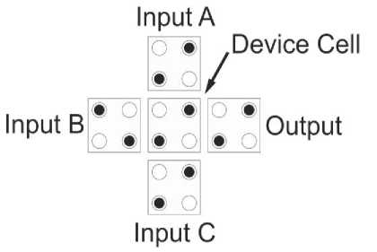
Fig.3. Three-Input Majority Gate
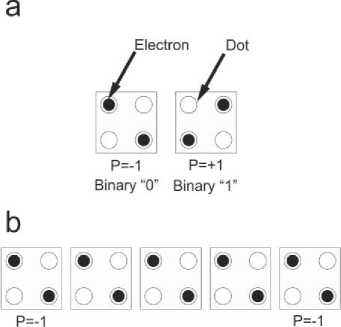
Fig.1. (a) Basic cell (b) QCA wire
QCA circuits can be synchronized by dividing into clock zones with at least two cells in each of them [3]. This property, enables the designers to implement parallel QCA circuits by employing a four-phase system (Switch, Hold, Release and Relax) which trace all the zones one after the other as is shown in Fig. 4. During the Switch phase, cell polarization would be changed based on the neighboring cell polarizations. In the Hold phase, cell polarization is high and as the result cell keeps its polarization and only can affect other cells which are determined in Switch phase. During the next two phases, cells lose their polarizations until the next Switch phase [4, 6]. As is noted in [3], a synchronized three-input majority gate with a robust structure can be achieved when the middle cells have been adjusted in a clock zone after the input cells and in a clock zone before output cell.
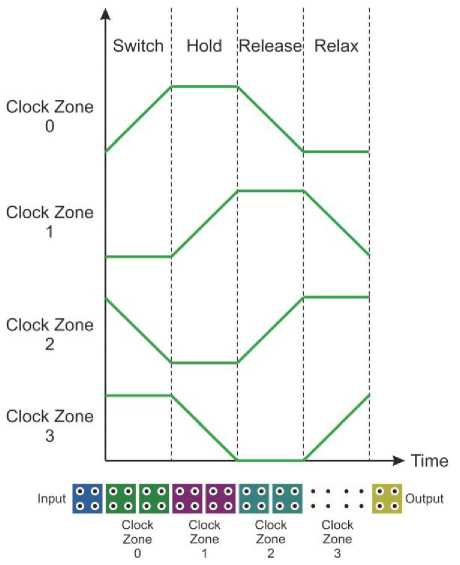
Fig.4. QCA Clock Phases in a Clock Zone
about 0.14 µm 2 with 102 QCA cells, therefore, as reported in [5], a 4-bit counter consumes 1130 cells in 2.2 µm 2 area. As is illustrated in Fig. 7, another attempt has been made in [14] in which 90 cells are exploited for implementing a QCA JK flip-flop. Besides, this design takes over 0.1 µm 2 area, so a 4-bit counter consumes 652 cells in 0.74 µm2 area.
Clock ^
-1.00 ".^^
ШЩШЖЩШГО®• еешшшшеешшшее • ggEEEEEEEE Щ
EEEEBBBQEB ЕЕ
SB H^
• щщщщ ЕЕШЕЕНЗ 1 ■ • • щщщ • • EEEE
-1.00
Fig.6. QCA JK Flip-Flop used for Constructing N-Bit Counters in [5]
-
III. Q ca C ounter A rchitectures
In this section, the previous designs for QCA counters are inspected. As is discussed in [5-8,14], designing memory elements using QCA cells provides a considerable optimization in contrast to conventional CMOS technology. A QCA loop containing four sequential clock zones (1 clock cycle) can be considered as a memory cell for storing one-bit data [5] (Fig. 5). The inherent capability of the QCA cells resulted in the QCA loop has streamlined the implementation of sequential circuits such as flip-flops [7]. Hence, several designs for diverse counters can be found in the literatures.
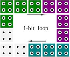
Fig.5. A Memory Element for Saving one Bit
Most of the recently reported researches have focused on the implementation of counters based on one of four-type of flip-flops [5]. The authors of [5] have designed mod4, mod8 and mod16 counters using a new level sensitive JK flip-flop cascaded with a proper level converter to realize an edge triggered JK flip-flop. As is shown in Fig. 6, this single block occupies a large area
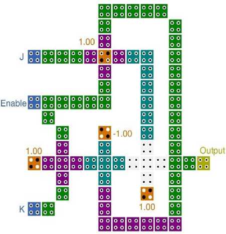
Fig.7. A QCA JK Flip-Flop used for Constructing N-Bit Counters in [14]
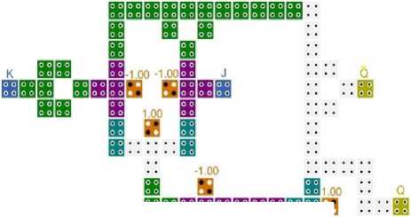
The authors of [8] with neglecting commonly used flip-flops have proposed an approach for designing counters by employing the explicit attribute of QCA loop. In this approach, QCA loops with different transmission delays are employed to realize a digital counter. Nevertheless as is shown in Fig. 8, there are several disadvantages with the suggested 4-bit counter in [8] which decrease the practical aspect of this design.
As is clear in this figure, the planned input and output cells are surrounded by the loops, so it is impossible to access them in a single layer. Moreover, the robustness of applied three-input majority gates is not considered which leads to increasing the noise effects on the circuit.
D 8СЭ
^g^g^g • • • • ■ - НН ИЯ ЯЯ ¥У^ НН ЯП ЯП ЯН НН ...... ЕШЩЗ^В
ЕЕ ее
-
• • • • • • • • ■ « • • • •
8 B8C18 ::
-
• ••
:: 8 8 100 5 8 8 ::
-
• •• •
щ щ • • щ
EE EE ■ • • EE EE щ щ щ А щсо
EE EE • • EE EE EE • * EE EE
EE EE
ЕВ Й-] [$ -1.00 8 :: 8 8
EE ■ • 0000 ЭЭ GQ 00 00 0000 EE * *
-
• •*
:: 8 888::
. . . . С ЩС2 . .. .
...... ИН ИН ИИ 00 00 00 ЯН ОЯ 0E3 ИИ000И * *
8 -l oo $
EE EE EE EE
^g^g^g^g......^g^gt^g H3EE......000000
-
Fig.8. The Presented 4-Bit Counter Circuit in [8]
According to the above-mentioned concepts, two main approaches can be considered for counter implementation in QCA technology, conventional one with using efficient QCA flip-flops and new one using QCA loops. Apparently, the first approach uses up more QCA cell as well as area in contrast to second one. Conversely, the second approach consumes more clock cycles in comparison to conventional approach. As a result, there is a tradeoff between area and circuit latency parameters which should be taken into consideration upon using them in a distinct application.
-
IV. N ew I mplementation F or Q ca C ounters
Targeting to present a QCA-compatible architecture for counter circuits, a new modified implementation for 4-bit counter is proposed in Fig. 9. The proposed circuit is implemented in one active layer with a considerable cell count optimization when compared to the prior designs in [5, 8, 14].
As is clear in Fig. 9, the proposed design consists of four loops which the output bits are generated after 1, 2, 4 and 8 clock cycle respectively and makes the delay of entire circuit as 8 clock cycles. As is mentioned earlier, this design is implemented in one layer which the input signal (Rst) and all the output signals (b3, b2, b1, and b0) are accessible in a single layer.
The detailed operation of the proposed circuit can be described as follow: After resting the circuit by applying binary ‘0’ then ‘1’ to Rst cell, first loop including a three-input majority gate and an inverter starts inversing itself continually in one clock cycle. Simultaneously, the second loop start inversing its stored data frequently but with 2 clock cycles delay. The third and fourth loops also act like first loop but with a 4 and 8-clock cycle delays.
Therefore, considering all loops’ outputs, we can see a frequency division (by two) in each successive loops. As an instance, the second QCA loop has the half frequency of the first loop and so on.
From the structural point of view, it should be mentioned that all the three-input majority gates take the advantage of having robust structure. Besides, by employing only one control signal, the hardware overhead due to the four control inputs (one input per each loop) is eliminated.
-
V. S imulation A nd C omparison
We examine the proper functionality of our proposed structure using QCADesigner tool version 2.0.3 as a popular simulation tool in QCA studies [9]. Both simulation engines (Coherence vector and Bistable approximation) are used to analyze the output’s waveforms. Table I shows the applied parameters in Coherence vector engine. Fig. 10 proves our claim about the precise operation of the proposed 4-bit counter. As is obvious in the bus created from Binary outputs (b3b2b1b0), the counting operation is correctly performed. As mentioned earlier, according to the considered “0” value for Rst signal, the first meaningful waveform for all units is revealed after 8 clock cycles. The red square in this figure is considered to show all valid outputs.
Evidently, in the achieved simulation waveforms, b3 has the lowest rate of changes (from ‘0’ to ‘1’ and vice versa) with 8 clock cycles delay and b0 has the highest rate with 1 clock cycle. As noted earlier, the output frequencies of b3, b2, b1, and b0 are successively doubled due to their loop latencies. It is worth mentioning that the high-polarized output cells (b3, b2, b1, and b0) are achieved by considering at least two cells in each clock zones as shown in Fig. 9.
Table 1. Coherence Vector Applied Parameters
|
Parameter |
Value |
|
Temperature |
1.000000 K |
|
Relaxation time |
4.1356675e-14 s |
|
Time Step |
1.000000e-016 s |
|
Total Simulation Time |
7.000000e-011 s |
|
Clock High |
9.800000e-022 J |
|
Clock Low |
3.800000e-023J |
|
Clock shift |
0.000000e+000 |
|
Clock Amplitude Factor |
2.000000 |
|
Radius of Effect |
80.000000 nm |
|
Relative Permittivity |
12.900000 |
|
Layer Separation |
11.500000 nm |
The comparison result between our presented 4-bit counter and the proposed circuits in [5, 8, 14] is prepared in Table II. Clearly, our proposed single layer four-bit counter surpasses all previously published circuits from need-to-wire crossing point of view. Additionally, it consumes least QCA cells in comparison to other designs. Although the presented design in [8] takes over less area occupation in contrast to our design, it suffers from high number of control inputs and consumed cell.
Table 2. Comparison Results
|
Desi gns |
Number of control inputs |
wire crossing |
Complexit y (cell) |
Circuit area (µm2 ) |
Delay (clock cycle) |
|
In [5] |
1 |
Yes |
1130 |
2.2 |
7 |
|
In [14] |
1 |
Yes |
652 |
0.74 |
2 |
|
in [8] |
4 |
Yes |
232 |
0.20 |
8 |
|
Fig. 7 |
1 |
No |
183 |
0.24 |
8 |
-
VI. C onclusion
In this paper, a novel efficient quantum-dot cellular automata 4-bit counter was proposed. This design was implemented based on a QCA-compatible approach without using the flip-flops as the main components. The presented design had distinguished superiorities over the best previously published circuits such as single layer accessibility to the input and output cells in addition to consuming less cell count. To authenticate the correct functionality of the proposed design, QCADesigner’s engines (Coherence vector and Bistable approximation) were employed and similar results were achieved.
-
VII. F uture W orks
In this work, inherent capabilities of QCA technology motivates us to design high performance counter circuits. As discussed earlier, although our proposed design utilizes more clock cycles for calculating precise output in contrast to conventional counterpart designs, it likewise dominates them in different point of views such as number of consumed cell and area occupation. Therefore, applying the inherent capability of QCA loops for designing other single layer sequential circuits or memory-based elements can be considered as future works.
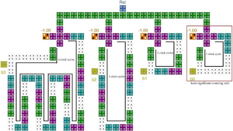
Fig.9. New QCA Single Layer Implementation for 4-Bit Counter
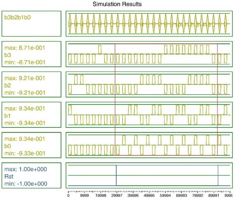
Fig.10. Simulation Results of Proposed QCA 4-bit Counter
References Designing Counter Using Inherent Capability of Quantum-dot Cellular Automata Loops
- P. D. Tougaw and C. S. Lent, "Logical devices implemented using quantum cellular automata," Journal of Applied physics, vol. 75, pp. 1818-1825, 1994.
- C. S. Lent and P. D. Tougaw, "A device architecture for computing with quantum dots," Proceedings of the IEEE, vol. 85, pp. 541-557, 1997.
- K. Kim, K. Wu, and R. Karri, "Towards designing robust QCA architectures in the presence of sneak noise paths," in Proceedings of the conference on Design, Automation and Test in Europe-Volume 2, 2005, pp. 1214-1219.
- V. Vankamamidi, M. Ottavi, and F. Lombardi, "Two-dimensional schemes for clocking/timing of QCA circuits," Computer-Aided Design of Integrated Circuits and Systems, IEEE Transactions on, vol. 27, pp. 34-44, 2008.
- X. Yang, L. Cai, X. Zhao, and N. Zhang, "Design and simulation of sequential circuits in quantum-dot cellular automata: Falling edge-triggered flip-flop and counter study," Microelectronics Journal, vol. 41, pp. 56-63, 2010.
- S. Angizi, S. Sarmadi, S. Sayedsalehi, and K. Navi, "Design and evaluation of new majority gate-based RAM cell in quantum-dot cellular automata", Microelectronics Journal 46(2015) 43-51.
- S. Angizi, K. Navi, S. Sayedsalehi, and A. H. Navin, "Efficient Quantum Dot Cellular Automata Memory Architectures Based on the New Wiring Approach," Journal of Computational and Theoretical Nanoscience, vol. 11, pp. 2318-2328, 2014.
- H. Aghababa, M. H. Yazdinejad, A. Afzali, and B. Forouzandeh, "Simplified quantum-dot cellular automata implementation of counters," in Devices, Circuits and Systems, 2008. ICCDCS 2008. 7th International Caribbean Conference on, 2008, pp. 1-4.
- K.Walus, T. J. Dysart, G. A. Jullien, and R. A. Budiman, "QCADesigner: A rapid design and simulation tool for quantum-dot cellular automata," IEEE Trans. Nanotechnol., vol. 3, no. 1, pp. 26–31, Mar. 2004.
- S. Sarmadi, S. Sayedsalehi, M. Fartash, and S. Angizi, "A Structured Ultra-Dense QCA One-Bit Full-Adder Cell", Quantum Matter 5, pp. 125-130, 2016.
- S. Sheikhfaal, S. Angizi, S. Sarmadi, M.H. Moaiyeri, and S. Sayedsalehi, "Designing efficient QCA logical circuits with power dissipation analysis", Microelectronics Journal, 46(2015) 462-471.
- K. Walus and G. A. Jullien, "Design tools for an emerging SoC technology: Quantum-dot cellular automata", Proceedings of the IEEE 94, 1225 (2006).
- G Varga, "Investigation of possibility of high temperature quantum dot cellular automata", Journal of Physics: Conference Series 61, 1216 (2007).
- S. Sheikhfaal, K. Navi, S. Angizi, and A. Habibizad Navin, "Designing High Speed Sequential Circuits by Quantum- Dot Cellular Automata: Memory Cell and Counter Study", Quantum Matter 4, pp. 190-197, 2016.
- S. Angizi, F. Danehdaran, S. Sarmadi, S. Sheikhfaal, N. Bagherzadeh, and K. Navi, "An Ultra-High Speed and Low Complexity Quantum-dot Cellular Automata Full Adder", Journal of Low Power Electronics, Vol. 11, No. 2, pp. 173-180, 2015.
- S. Sayedsalehi, M. Azghadi, S. Angizi, and K. Navi, "Restoring and non-restoring array divider designs in Quantum-dot Cellular Automata", Information sciences, 311, pp. 86-101, 2015.
- C. S. Lent and P. D. Tougaw, "A device architecture for computing with quantum dots," Proceedings of the IEEE, vol. 85, pp. 541-557, 1997.
