Development of a multilayered hybrid power divider

Author: Dudarev N.V., Darovskih S.N.
Section: Инфокоммуникационные технологии и системы
Article in issue: 1 т.17, 2017.
Free access
The paper proves a real possibility of designing the microwave electronic devices based on multilayer structures. The advantages of such design compared with a traditional application of the microstrip lines are demonstrated by an example of a hybrid microwave power divider (hybrid ring). The calculations of a multistructure-based hybrid ring presented in the paper allow forecasting a substantial decrease of the weight and size parameters for the microwave electronic devices. That provides their wide application in mobile and small-sized radio systems with a microwave informational channel. The weight and size problem is especially relevant for the devices like the various mobile on-board radars. This makes it possible to predict scientific and industrial relevance of the development.
Microwave modules, weight and size characteristics, multilayer technology, hybrid ring, slot line
Short address: https://sciup.org/147155170
IDR: 147155170 | UDC: 621.372 | DOI: 10.14529/ctcr170104
Разработка гибридного делителя мощности на многослойной структуре
В статье доказывается реальная возможность проектирования устройств сверхвысокочастотной (СВЧ) электроники на основе многослойной структуры их построения. На примере гибридного СВЧ-делителя мощности (гибридного кольца) показаны преимущества такого проектирования в сравнении с традиционными подходами, основанными на использовании микрополосковых линий. Приведенные в статье расчеты гибридного кольца на основе многослойной структуры позволяют сделать прогноз о существенном уменьшении массогабаритных характеристик устройств СВЧ-электроники, что обеспечивает возможность для их широкого использования в мобильных и малоразмерных радиотехнических системах с СВЧ каналом передачи и приема информации. Особенно актуальна проблема массогабаритных характеристик для таких устройств, как бортовые радиолокационные станции различного рода подвижных объектов. Это позволяет прогнозировать научную и производственную актуальность данной разработки.
Text of the scientific article Development of a multilayered hybrid power divider
A variety of the modular microwave devices such as couplers, bridge circuits, and matched dividers are widely used in a microwave equipment to control a signal in a microwave path. The major drawback of these devices is the directly proportional relationship of their weight and size characteristics and a working frequency range. While the mass-dimensional characteristics are not very significant for the stationary objects such as terrestrial radar systems, the weight and size savings become vital for microwave devices set on the mobile objects. Consequently, the development a microwave technology targeting to the weight and size decrease is a topical problem. Nowadays solutions are based on the microstrip technology, which applies the methods of magnetic sputtering, hybrid hook-up elements, and dielectrics with high relative dielectric constants [1]. However, the potential of the technology in decreasing the weight and size characteristics of microwave devices is limited by their single-layer architecture. Therefore, it seems appropriate to consider developing microwave electronic devices based on their multilayer structure.
Let us estimate the advantages of the devices developed with the use of multilayer technology considering an example of microwave power divider (hybrid ring). Its weight-size and electric characteristics compared with those of a device traditionally designed by microstrip technology would allow the conclusion that the multilayer technology is advanced to develop the microwave electronic devices.
-
1. Design of a microwave divider based on a microstrip technology
A bridge circuit of the microwave power divider (hybrid ring) (Fig. 1) in its traditional single-layer performance is widespread in the microwave radiotechnical systems.
Its calculation [2, 3] reduces to determining a mean diameter d mean and ring width W k at the known values of a microstrip line width W , wave resistance Z 0 , effective dielectric permeability ε ef , main transmission line (1–4), operation frequency (wave-length λ 0 ), and other benchmark data and requirements applicable to the power divider. The basic relations for calculating the parameters of a hybrid ring are the following [2–5]:
d mean = 2^^7Й 7 , (1)
where ε ef is an effective dielectric permittivity. For a microstrip line, it is calculated using a formula
—1
£ «/ = £^ + £^ (1+10^' ’ , (2)
where ε r is a relative dielectric permittivity of the dielectric base, W is a width of a microstrip line, and h is a thickness of the dielectric.
200(1— В ) W = h\—
Z o V^ r
, Г: ^ = ^1-
'200(1- ^ ) Z k V^
-11
-l],
where Δ is a metallization thickness, Z 0 is an input wave resistance, and Z k is a wave resistance of the ring.
zk = Z 0 V2. (5)
Яо
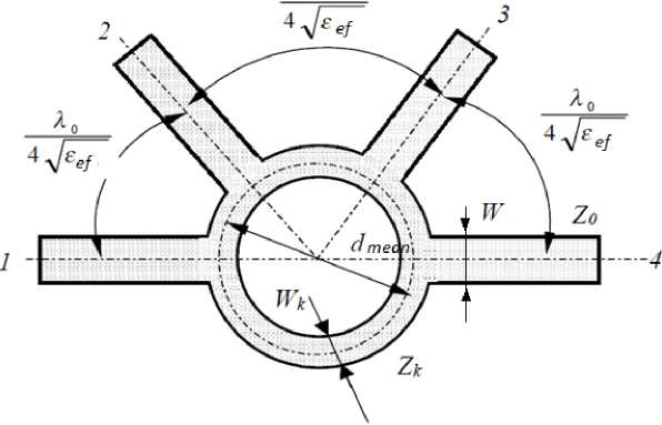
Fig. 1. Hybrid ring
When using the formulas (1)–(5), the values of the hybrid ring parameters such as d mean = 45 mm and W k = 1.7 mm were obtained for the following conditions: frequency range was 945–970 MHz, the width of a microstrip line W = 3.52 mm, the input wave resistance Z 0 = 50 Ohm, and the base material was double-sided laminated dielectric RO4003.
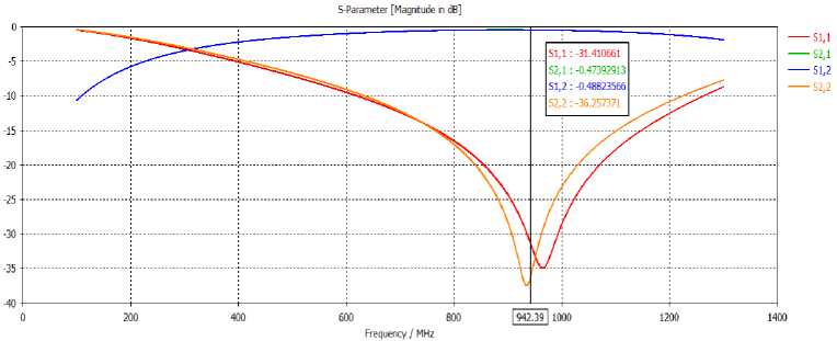
To evaluate a correspondence between electromagnetic characteristics of the calculated hybrid ring (Fig. 2) and those specified for an even division of a signal power (–3 dB), reflection factor and electromagnetic decoupling not less than 20 dB in the range 945–970 MHz, the user’s CAD system CST Microwave Studio was utilized.
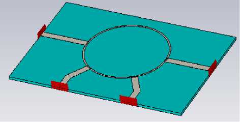
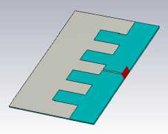
Fig. 2. Single-layer topology of a hybrid ring model
As a result of calculations using CAD, the electromagnetic characteristics of the device has been obtained. The diagrams of the scattering matrix elements are the most illustrative (Fig. 3). Analysis of the diagrams really gives exhaustive information we need to know about the electrical characteristics of microwave modules in design engineering. On the ground of calculation of the main electromagnetic characteristics for the hybrid ring with the mentioned parameters (Fig. 3), the following conclusions could be done in accordance with the scattering matrix graphs.
-
• The device provides an even division of the channel 1 signal power by the channels 3 and 4 ( S 31 , S 41 = –3 dB) in a broad band (950–1000 MHz).
-
• Decoupling in the same band varies from –25 dB on the band edges to –40 in its centre.
-
• The reflection factor ( S 11 ) in the band 950–1000 MHz varies from –25 dB on the band edges to –32 in the centre.
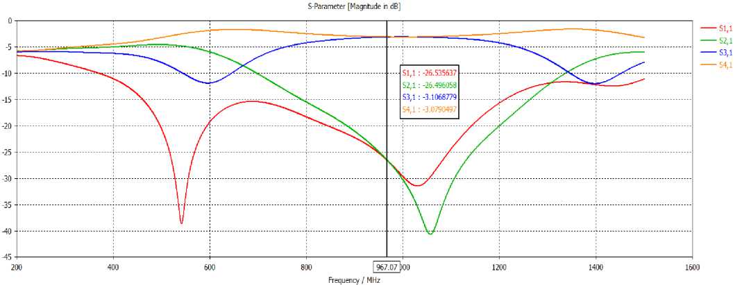
Fig. 3. Amplitude characteristics of the hybrid ring by the microstrip technology, where S 31 and S 41 are the power dividing coefficients, S 21 is a decoupling factor between 1 and 2 inputs of the device, and S 11 is a first input reflection factor
The characteristics show that the device can operate not only in the frequency band 945–965 MHz predetermined when calculating but also in the much wider band 950–1000 MHz with keeping all the main requirements to the device such as even division of the signal power by the channels ( S 31 , S 41 = –3 dB), the value of decoupling, and reflection factor not less than –20 dB.
-
2. Multilayered hybrid ring
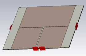
To implement the hybrid ring based on the multilayer structure, the overall size calculated above are used. In a space of decoupled input arms, the divider is decomposed into two parts and placed on several dielectrics (Fig. 4). Two clad dielectrics RO4003 are used. The dielectrics fit together and each half of divider is placed on the outside. Metallization between two dielectrics acts as a shield. The openings for the jumpers connecting the parts of the hybrid ring are etched in the shield (Fig. 4).
In addition, the size 100 × 70 × 1.52 mm of device specifies its volume equal to 10 640 mm3 (excluding the shielding case). A width of air space from a transmission line to a metal shield should be not less than three widths of a dielectric for the microstrip line. Consequently, the real volume of the product in case is 42 560 mm3 (10 640 × 4 mm3).
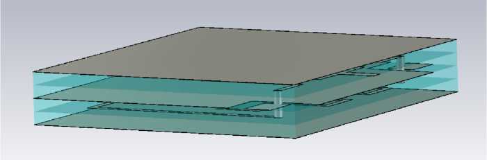
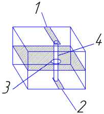
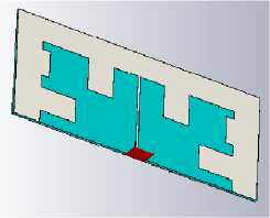
Fig. 4. A model of themultilayered divider with the jumpers. 1 and 2 are the transmission lines, 3 is via opening, and 4 is a jumper
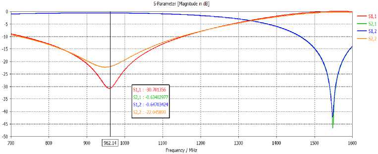
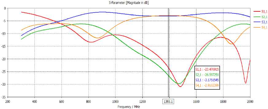
It follows from the calculation of the main characteristics of the multilayered hybrid ring (Fig. 5) that the multilayered power divider matches its single-layered analogue in amplitude characteristics while it is approximately 6 times more compact (size is 40 × 40 × 4.56 mm (7296 mm3)). As the device is implemented on the symmetrical line, the shielding case is situated back-to-back with the product (an impact of the case on the total volume of a product is neglectable).
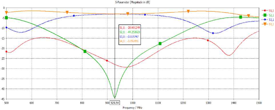
Fig. 5. Amplitude characteristics of the multilayered hybrid ring depending on a frequency
A shortcoming of such hybrid ring is existence of the openings. The shortcoming may be viewed in different ways such as technological and electrodynamical ones. In terms of technology, the openings imply the whole range of additional operations. Naturally, the openings are not an unsolvable problem. Today the process of obtaining the via openings is mastered and applied successfully to produce the low-frequency cards. In terms of thermodynamics, a jumper is a specific kind of transmission line (waveguide), so it should have a wave resistance about 50 Ohm. The layers may be connected by a slot line (Fig. 6).
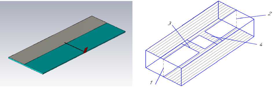
Fig. 6. A model of a volume slot line. 1 and 2 are coupled regions (slots), 3 and 4 are transmission lines
Instead of a jumper, in the hybrid ring it is possible to use a volume slot line, which consists of two metalized zones on opposite sides of a clad dielectric. Depending on the overlap value, it is possible to obtain a slot line with definite wave resistance.
Analysis of the calculation results for the amplitude characteristics of a volume slotted junction (Fig. 7) allows for the conclusion that the junction could be used in low-band devices permitting the signal bandwidth, which does not exceed 10 % of the carrier frequency value. The key feature of a slot line is its length, which should be equal to a quarter or one eighth part of the wavelength. For space saving, the slot lines are assembled in meander structures and their transit characteristics are compared with those of the previous model (Fig. 8 and 9).
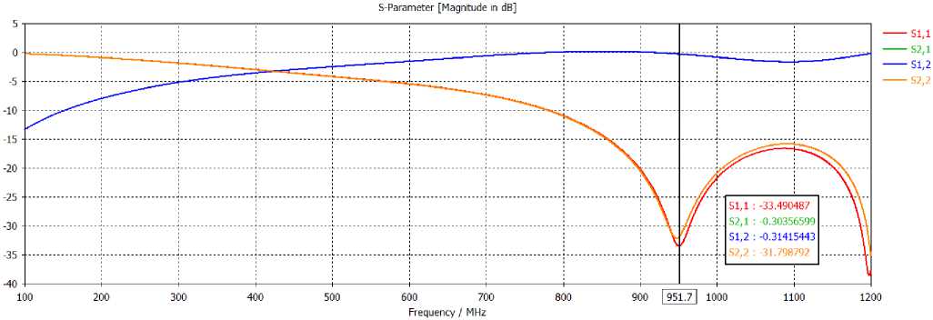
Fig. 7. Amplitude characteristics of a volume slotted junction
b)
Fig. 8. A model of a volume slotted junction assembled in a periodical meander structure (a), and its amplitude characteristics (b)
a)
b)
Fig. 9. A model of a volume slotted junction with a complex structure (a), and its amplitude characteristics (b)
a)
Being compared, the amplitude characteristics of the junctions (Fig. 7–9) demonstrate that while the number of the spot line creases grows, a marginal deterioration of the reflection factor and inconspicuous decrease of a routing signal value takes place.
A model of a hybrid ring implementation based on an elementary slot line without creases is presented in Fig. 10.
The hybrid ring has the overall size 70 × 50 × 3.04 mm (10 640 mm3).
A design process for each of the devices described above was performed in accordance with the following algorithm presented as a flow chart (Fig. 11).
b)
Fig. 10. A model of a hybrid ring with volume slot lines (a) and its amplitude characteristics (b)
a)
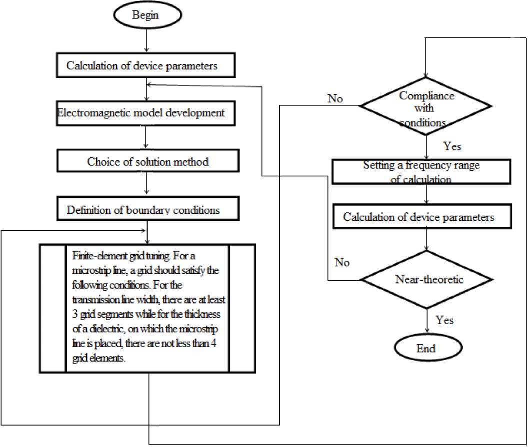
Fig. 11. A flow chart of a process algorithm for designing the microwave electronic devices
Conclusion
The paper introduces the multilayer technology to implement the microwave electronic devices such as directional couplers, phase shifters, filters, various power dividers, and combiners, etc. The application of the technology allows making a real progress in achieving weight-size minimum. It has been demonstrated by the example of the hybrid ring implemented in both traditional microstrip and multilayered constructs. With equal level of the electrical characteristics, the multilayered hybrid divider has a volume 6 times less than the microstrip one.
A significant advantage of the technology is a feasibility of a high packing density for the complex radiotechnical devices using the microwave electronic components.
References Development of a multilayered hybrid power divider
- Малорацкий, Л.Г. Микроминиатюризация элементов и устройств СВЧ/Л.Г. Малорацкий. -М.: Сов. радио, 1976. -216 с.
- Справочник по расчету и конструированию СВЧ полосковых устройств: справ./С.И. Бахарев, В.И. Вольман, Ю.Н. Либ; под ред. В.И. Вольмана. -М.: Радио и связь, 1982. -328 с.
- Малорацкий, Л.Г. Проектирование и расчет СВЧ элементов на полосковых линиях/Л.Г. Малорацкий, Л.Р. Явич. -М.: Сов. радио, 1972. -232 с.
- ГОСТ 21702-76. Устройства СВЧ. Полосковые линии. -М: Изд-во стандартов, 1977. -4 с.
- Фельштейн, А.Л. Синтез четырехполюсников и восьмиполюсников на СВЧ/А.Л. Фельдштейн, Л.Р. Явич. -2-е изд. -М.: Связь, 1971. -385 с.
