Digital Twin Aggregated into a High-Efficiency Charge-Discharge Device of the Power Supply System of a Spacecraft

Author: Krasnobaev Yu.V., Golubev E.A., Korshun K.V., Yablonsky A.P.
Journal: Siberian Aerospace Journal @vestnik-sibsau-en
Section: Aviation and spacecraft engineering
Article in issue: 2 vol.26, 2025.
Free access
The power supply system (PSS) of a spacecraft (SC) is one of its most critical systems. The generation of electrical energy in modern SC PSS is typically carried out by solar panels (SP). In the absence of energy generation from the SP or during periods of low energy output, the necessary electrical energy is supplied to the load from battery packs (BP) through a charge-discharge device (CDD). Usually, the CDD is connected in parallel to the output buses of the PSS and, in battery discharge mode, provides stable voltage to the load. The replenishment of energy in the BP — its charging — occurs during time inter-vals when the energy generated by the SP exceeds the energy consumed by the load. Additionally, the CDD can provide voltage stabilization at the load. The article presents the power circuit of a pulse converter capable of reversing the flow of energy and operating in a buck-boost mode with high efficiency. It is shown that using the power circuit of this pulse converter in the CDD of SC power supply systems can improve several of their characteristics, namely, energy-mass and reliability metrics, enhance efficiency, and improve the quality of the output voltage of the PSS while reducing the level of generated electromagnetic interference. The article includes research results on the CDD, with the power section designed according to a prom-ising scheme obtained using a simulation model and a physical prototype. It is demonstrated that the synthesized control law allows for maintaining the astatism of the output voltage and a short duration of tran-sient processes. However, it was found that the simulation model of the CDD provides a shorter duration of transient processes compared to the physical prototype. This is explained by the fact that due to the short time interval during which the controlling microcontroller must perform calculations for switching mo-ments of the power transistors, the mathematical expressions used for calculations had to be simplified. The aim of the work is to find a technical solution for generating control signals that allows for the elimination of complex mathematical calculations of the switching moments of the power transistors in realtime. To achieve this, it is proposed to precalculate the switching moments of the power transistors for the entire range of power transmitted through the CDD and for the entire range of possible voltages on the BP. The obtained values of the switching moments of the power transistors in the form of tables should be recorded in the memory of the microcontroller controlling the power circuit of the CDD and used for control purposes. The article discusses the methodology for obtaining tables of switching moments for the power transis-tors of the CDD, which essentially serve as a digital twin of the CDD, and provides an example of such tables.
Power supply system, battery pack, pulse voltage converter, charge-discharge device, digital twin
Short address: https://sciup.org/148331243
IDR: 148331243 | UDC: 621.314 | DOI: 10.31772/2712-8970-2025-26-2-239-251
Text of the scientific article Digital Twin Aggregated into a High-Efficiency Charge-Discharge Device of the Power Supply System of a Spacecraft
The most important service system of a spacecraft (SC) is a power supply system (PSS). It is designed to generate electrical energy, its storage and the supply of electrical energy of a given quality to target energy consumers and other service systems of a spacecraft during its entire active life [1]. The generation of electrical energy in modern PSSs of a SC is usually carried out by battery packs (BP); and specified voltage quality on the load is provided by pulse voltage stabilizers (PVS). If there is no generation of energy from BPs or if the level of generated energy is low, the required electrical energy is transferred to the load from storage batteries (SB) through a charge-discharge device (CDD). Normally, a CDD is connected in parallel to the output busses of a PSS and in the discharge mode of a BP it provides stable tension on the load. BP energy replenishment is when its charge occurs at time intervals when the energy being generated by a BP exceeds the energy being consumed by the load. In this case a CDD can also provide voltage stabilization on load [2-4].
Advanced charge-discharge device
A charge-discharge device is by definition a pulse voltage converter and it has a set of requirements for energy mass characteristics, performance, reliability, ability to provide the required quality of voltage at the output of a PSS, low level of generated electromagnetic interference and a number of other characteristics. A buck-boost reversible pulse converter (RPC) [5-8] has the ability to provide the best performance for all the above-mentioned set of requirements. Its circuit diagram is shown in Figure 1.
The power chain of an RPC can be connected by side 1 to a BP, and by side 2 to the output busses of a PSS. The symmetry of an RPC power chain makes it possible to reverse the energy flow with the corresponding change in the switching algorithm of the RPC power keys executed on VT 1 – VT 4 transistors, and to ensure both the PB charge and the stabilization of the PSS output voltage at the BP discharge. Thus, one set of electrical radio elements provides both modes of operation of a CDD and significantly increases the energy mass characteristics of a CDD [7; 8]. In addition, the small number of electrical radioelements in an RPC improves its reliability.
High performance of this converter, in a number of modes exceeding 99%, is ensured by the method of control of power transitors [5; 6] called by its authors ‘new strategy of modulation.’
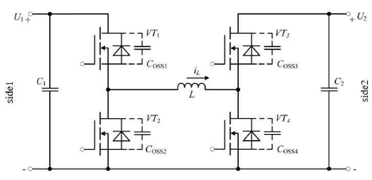
Рис. 1. Схема силовой цепи реверсивного импульсного преобразователя (РИП)
Fig. 1. Circuit diagram of the reversible pulse converter (RPC)
A new transistor switching strategy proposed in [5; 6] allows combining the advantages of converters with pulse-width modulation (PWM) in terms of good adjustment characteristics, and resonant converters in terms of providing high performance. The new switching strategy is that each of the pairs of transistors VT1 – VT2 and VT3 – VT4 forms some delay of the transistor activation relative to the moment of the pair’s transistor activation by tdel. This delay in the activation of a pair transistor looks like «dead» time needed to eliminate through currents in similar transistor inverters [9], but its purpose is different. After switching off one of the pair transistors, an oscillatory process begins in the LC-circuit formed by the inductance of the L throttle and parasitic capacitances Coss of the power transistors. After the tdel time expires, the parasitic capacitance Coss of the switched-off transistor is discharged; the voltage sign on this transistor changes and the technological diode of the transistor is unblanked. In this case, the voltage on the transistor is equal to the voltage on an open technological diode and does not exceed one volt. At this voltage, the transistor is switched on without dynamic losses in «soft switching» mode. Switching off the transistor at a voltage close to zero in the ‘soft switching’ mode is provided by the discharged parasitic capacitance Coss of the switched transistor [10]. Providing «soft switching» modes for transistors allows reducing the level of electromagnetic interference generated by RPCs and improving reliability by decreasing the thermal loads on the transistors.
The required quality of the voltage at the RPC output, namely the short duration of the transition processes and the astatism of the output voltage, is provided by the synthesis of the pulse duration law of controlling the power transitors of an RPC using the developed method of bringing the system with a PWM to the system with a pulse-amplitude modulation (PAM) [11]. This method makes it possible to apply polynomial equations of synthesis and to provide the minimum possible duration of transition processes and astatism of output voltage in an RPC [12; 13].
Figures 2 and 3 show timing diagrams of the iL current of the L throttle of the RPC and the control signals U contr .VT 1 – U contr .VT 4 by the transitors VT1 – VT4, respectively. The difference between the figures is that in Figure 2 the timing diagrams are shown when the RPC works in high power transfer mode, and in Figure 3 it works in low power transfer mode. When the RPC works, the t1 time is modified by the synthesized law of PAM, the t 2 time is calculated in mathematical terms, and the t 3 time is set by a comparator, which actuates at the moment when the iL current of the L throttle is equal to the I 0 value of the reverse current of the L throttle. This reverse current I 0 of the throttle has a negative value and is closed through the open transistors VT2 and VT4 on the time interval t 3 - T. This current of the L throttle of reverse direction slightly reduces the performance of the RPC because of static losses in the transistors and the throttle itself, but it allows ensuring the process of recharging the parasitic capacitances C oss of the transistors and exclude dynamic losses. The value of this current is determined by the condition [5; 6]:
To test the synthesized control law, an RPC simulation model has been developed. In the RPC model the t1 time changes according to the synthesized law of PWM, the t2 time is calculated by mathematical expressions using a graph-analytical method for solving equations, and the t3 time is set by a comparator, which actuates at the moment of equality of the iL current of the L throttle to the I0 value of reverse current of the L throttle.
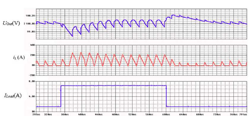
The timing diagrams illustrating the transient processes in the RPC obtained by computer modelling are shown in Figure 4. The conversion frequency in the RPC is chosen to be 50 kHz; the capacitance of the output filter is 500 μF, and its internal active resistance is 0.006 Ohm. The voltage on AB (side 1 ) is assumed to be 65 V, and at the output of the voltage pulse converter (side 2 ) it is 100 V. The timing diagrams (from top downward) show the U out voltage at the output of the voltage pulse converter, iL current of the throttle of the voltage pulse converter and iL load current.
From the analysis of the timing diagrams it follows that the new steady state mode occurs after 100 ms and there is no static voltage stabilization error.
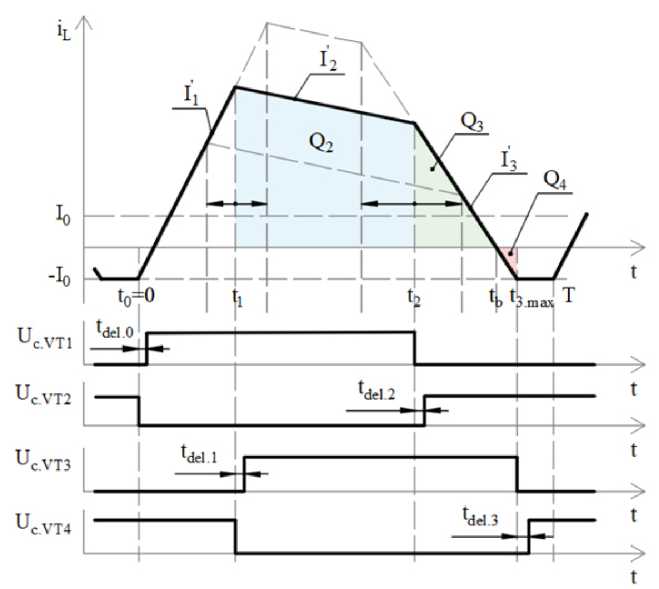
Рис. 2. Временные диаграммы тока i L дросселя РИП и сигналов управления транзисторами в режиме передачи большой мощности
Fig. 2. Timing diagrams of the inductor current i L of the RPC and control signals for the transistors in high power transfer mode
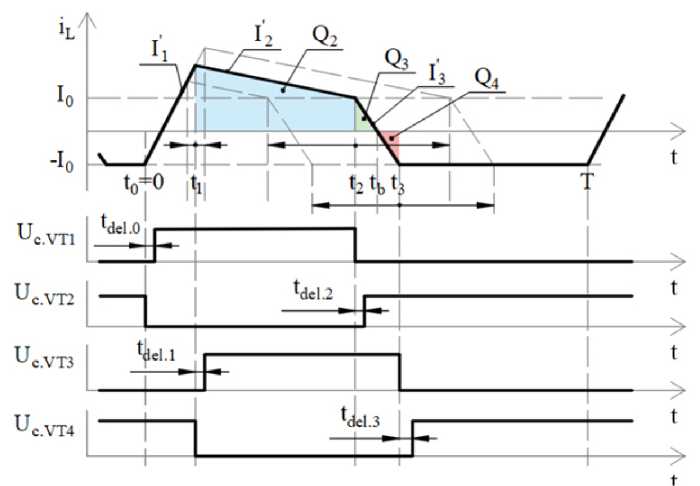
Рис. 3. Временные диаграммы тока i L дросселя РИП и сигналов управления транзисторами в режиме передачи малой мощности
Fig. 3. Timing diagrams of the inductor current i L of the RPC and control signals for the transistors in low power transfer mode
tfusj
Рис. 4. Временные диаграммы, иллюстрирующие переходные процессы в РИП
Fig. 4. Timing diagrams illustrating the transient processes in the RPC
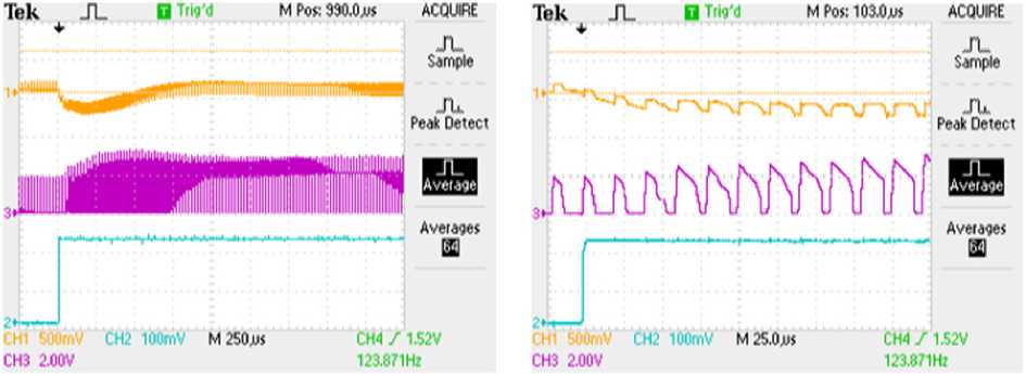
To check the feasibility of implementating the RPC being considered, its physical prototype with control from a microcontroller has been made. The power part of the RPC prototype is made according to the diagram shown in Figure 1, and has the following parameters: inductance of the throttle L = 8 µH, capacitance of the output capacitor C = 1000 µF, conversion period T = 20 ms. The voltage at the output of the RPC U out = 50 V and the voltage at the input U in = 45 V. In the RPC prototype, the microcontroller calculates the t 1 time (it changes according to the synthesized law of PWM) and the t 2 time (it is calculated mathematically using equations describing the trajectory of the current change of the L throttle [14]). The t 3 time is set by a comparator and actuates at the moment of equality of the i L current of the L throttle to the I 0 value of reverse current of the L throttle. The oscillograms illustrating the work of the RPC model are presented in Figure 5. The oscillograms (from top downward) show the U out voltage at the output of the voltage pulse converter (scale - 500 mV/div.), i L current of the RPC throttle (scale - 10 A/div.) and i L load current (2 A/div.) with step increase in load current. In Figure 5 a the selected scale on the time axis is 250 ms/div.; in Figure 5 b it is 25 ms/div.
а б
Рис. 5. Осциллограммы, иллюстрирующие работу макета РИП
Fig. 5. Oscillograms illustrating the operation of the RPС prototype
The comparison of the results of simulating transient processes in the RPC model shown in Figure 4 and the results of the experimental studies of transient processes in the RPC prototype showed that in both cases the astatism of the RPC output voltage is ensured. Nevertheless, the duration of the transient process from the moment of resentment to the moment of transition to the steady state mode in the RPC model is significantly longer. This is due to the fact that the time interval from the t 3.max time to the T time (see Figure 2) in the RPC model is taken to perform the computational procedures. This time interval, at the selected conversion period T = 20 ms and t 3.max = 0.9 T, equals 2 ms. Because of the short duration of this time interval, it is necessary to simplify mathematical expressions according to which the times t 1 and t 2 are calculated. This has led to an increase in the duration of the transient process and the amplitude of the RPC output voltage deviation.
Therefore, it can be considered relevant to find a solution that allows determining the exact values of the times t 1 and t 2 during small time intervals, in accordance with which switching transistors are supposed to be made [15]. An alternative solution to this problem can be the preliminary calculation of the times t 1 – t 3, where some P power averaged over the Т conversion period is transmitted to the output of the RPC. In this case, a system of tables should be obtained, where the value of P changes with some step and for each of its values the times t 1 – t 3 are given in the table. In addition to the step-by-step change of the P power value, the tables should show a step-by-step change of the voltage on the AB, i.e. on the side 1 of the RPC. The step-by-step voltage change on the AB shall cover the entire allowable range of the AB voltage change. The calculation of the values of the times t 1 , t 2 and t 3 is made for the parameters of the power chain of the RPC, namely the inductance of the L throttle, T conversion period and the accepted value I 0 of the reverse current of the L throttle. This tabular data system reflects the processes in the RPC and is essentially a digital twin of the RPC. Since this digital twin (DT) is planned to be entered into the memory of the microcontroller controlling the RPC, it can be defined as an aggregatable digital twin. The method of obtaining a digital twin of the RPC and the example of the DT are presented below.
The timing diagrams of the i L current of the RPC throttle and its transient control signals in modes when large and small power is transmitted through the RPC are shown in Figure 2 and Figure 3 respectively. The rates I′ 1 , I′ 2 and I′ 3 of changes in the i L current of the RPC throttle for the time intervals t 0 – t 1, t 1 – t 2 and t 2 – t 3 are found respectively by the following expressions [14]:
I′1 = UL.1 / L = U1 / L,(2)
I′2 = UL.2 = (U1 – U2) / L,(3)
I′3 = UL.3/ L = –U2 / L,(4)
where U1 and U2 is voltage on the sides 1 and 2 of the RPC respectively and L is RPC throttle induc- tance. In [14] using the expressions (2)–(4), the currents I1, I2 and I3 of the L throttle are determined for the times t1, t2 and t3 respectively:
I1 = I′1t1 = U1t1 / L,(5)
I2 = I1 + I′2(t2 – t1) = I1 + (U1 – U2)(t2 – t1) / L,(6)
I3 = I2 + I′3(t3 – t2) = I2 – U2(t3 – t2) / L.(7)
and the tb time, in which the iL current of the throttle is equal to zero, is determined as tb = t3 + I0 / I′3 = t3 + I0U2 / L.(9)
The energy transfer onto side 2 occurs in the time interval from t 1 to t 3.max . The areas of the figures shown in Figure 2 as Q 2 and Q 3 correspond to the charge transmitted during the T period onto side 2 ; and the area of the figure indicated in Figure 2 as Q 4 corresponds to the charge taken for the T period from side 2 . The charges Q 2 , Q 3 and Q 4 obtained using the expressions (5)-(9) are determined as
Q2 = (I1 + I2)(t2 – t1) / 2,(10)
Q3 = (tb – t2)I2 / 2,(11)
Q4 = (t3 – tb)I0 / 2.(12)
The net charge being transmitted by the RPC onto side 2 during the T period is determined as
Qtrans.2= Q2 + Q3 – Q4.(13)
The energy being transmitted by the RPC during the T period onto side 2 is defined by the expression
WT = Qtrans.2U2,(14)
and the power on side 2 of the RPC is defined as
P2 = WT / T.(15)
In low power transfer mode (see Figure 3) the t 2 time depends on the t 1 time and corresponds to the moment when the I 2 current is equal to the I 0 current. In this mode, the throttle current changes according to the timing diagrams shown in Figure 3 а , the rate of rise and fall of the throttle current is determined by the expressions (2), (3) and (4). This moment is calculated according to the expression:
t 2 = (2 I 0 L – t 1 U 2 ) / ( U 1 – U 2 ). (16)
In these conditions, the regulation of the power transmitted by the CDD to the BP charge is carried out only by the displacement of the t 1 time of switching the right pair of the transistors.
When the throttle current changes in accordance with the timing diagrams shown in Figure 3, the rate of rise and fall of the throttle current is defined by the expressions (2) and (4), respectively; and the net charge Q trans.2 transmitted over the T period onto side 2 is determined in the same way as in high power transfer mode using the formulae (10) - (13).
To determine the times t 1 , t 2 and t 3 for switching RPC transistors, an algorithm has been developed using the expressions (10)-(16). The block diagram of this algorithm is shown in Figures 6 and 7.
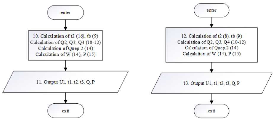
The calculation process using this algorithm is the following: in block 1 , the source data T , U 1 , U 2 , I 0 , t 1 , L , U step are introduced. Further the condition that the voltage on side 1 is less than the voltage on side 2 is checked. If it is true, the program proceeds to block 2 where the output parameter calculation subroutine for low power mode is called once. The subroutine consists of two blocks: 10 and 11 . In block 10 the switching moments of the RPC transistors, intermediate and net charges, energy and power being transmitted to side 2 are calculated. In block 11 the values obtained are written to a . csv . table. After completing block 2 , it is checked that the switching time t 3 is less than the maximum switching time t 3 .max. If this condition is true, the calculation of output parameters for low-power mode is repeated cyclically with an increase in the t 1 time after each cycle iteration. Once the condition is no longer valid, block 5 returns to the original t 1 and sets the maximum difference module between the times t 1 and t 2 . The program then cyclically calculates output parameters already for high-power transfer mode (blocks 7 , 12 , 13 ), also increasing t 1 after each iteration. Blocks 12 and 13 are similar to blocks 11 and 12 except that the time of switching t 3 is selected fixed. Once the maximum modulus of the difference between the times t 1 and t 2 is reached, we believe that the digital twin table for the current U 1 is obtained and in block 9 there is an increase in voltage on side 1 at a given step, after which the algorithm of the table is repeated, but already for the new U 1 .
As a result of the multiple program launch for different U 1 voltage values on side 1 of the RPC, which change with a given step, the values of the moments t 1 , t 2 and t 3 of switching the transistors of the RPC and the values of the corresponding to them Q charge transmitted to side 2 of the RPC for the T period and Р power on side 2 of the RPC are obtained. The obtained values of the moments t 1 , t 2 and t 3 of the Q charge and Р power are combined into a set of tables, an example of which fragmentarily for the voltage U 2 = 100 V on side 2 of the conversion period T = 20 ms and the inductance of the throttle L = 20 μH is shown in Figure 8. The complete set of such tables reflects energy conversion processes in the RPC, and is essentially a DT of the RPC. This DT can be used for modelling and process studies in the RPC, but its main purpose is to be integrated into an RPC feedback circuit in order to exclude calculations of the times t 1, t 2 and t 3, in which RPC transistors are switched. These DTs are called aggregatable.
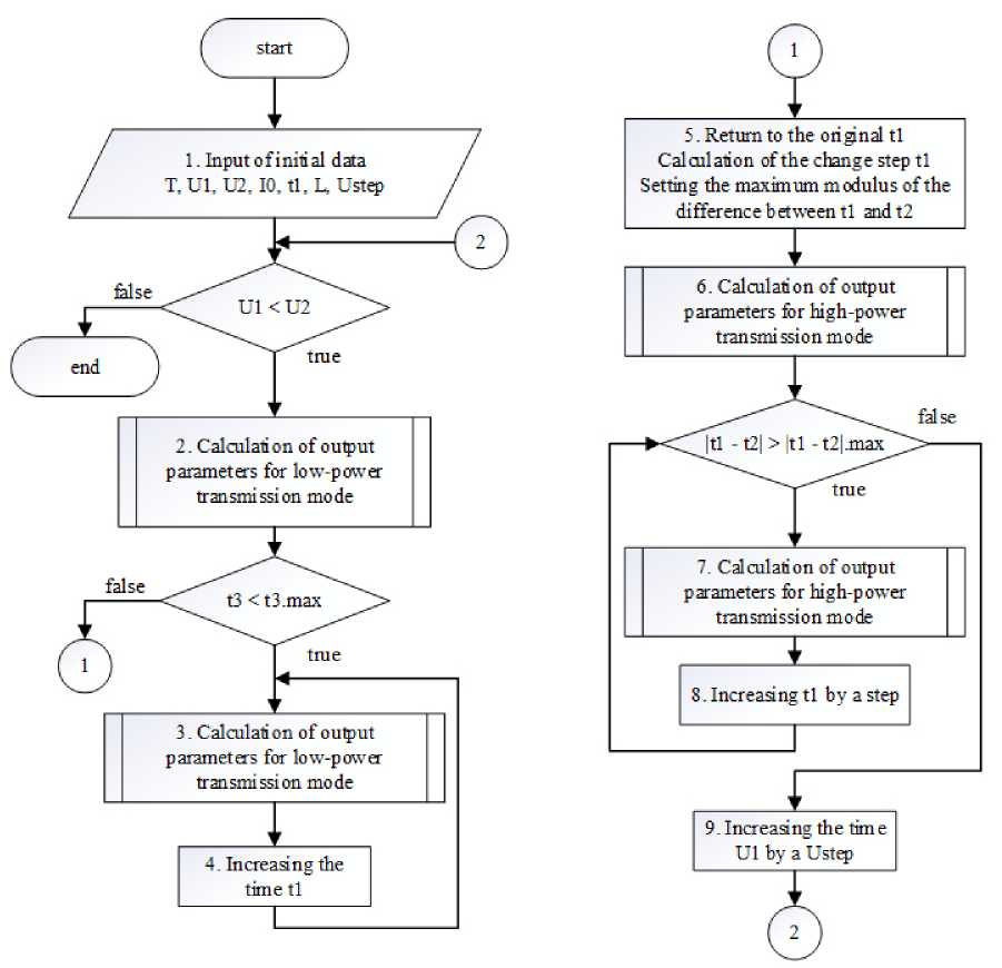
Рис. 6. Алгоритм получения таблиц для цифрового двойника
Fig. 6. Algorithm for generating tables for the digital twin
б
Рис. 7. Подпрограммы расчета данных при малой ( а ) и большой ( б ) передаваемой мощности
Fig. 7. Subroutines for data calculatiоn at low ( a ) and high ( b ) transmitted power
In addition to the times t 1 , t 2 , t 3 and the Q charge and Р power corresponding to them transmitted during the T period onto side 2 , the first table shows the length of the delays t del of the activation of the corresponding pair transistors in the vicinity of the times t 1 , t 2 and t 3 . The calculations are performed for the IRFB 4227 transistor parameters according to the methodology described in [10].
|
# |
£4 V |
US |
tl, US |
tb US |
tdtlQ, US |
td |
td |
tdflb US |
0. uC |
p, w |
||||||||||||||||||
|
1 |
75 |
1.00 |
2,40 |
2.80 |
0.21 |
0.18 |
0.21 |
0.21 |
2.63 |
13.13 |
||||||||||||||||||
|
2 |
75 |
1.11 |
2.85 |
3.25 |
0.21 |
0.18 |
0.21 |
0.21 |
3.63 |
18.15 |
||||||||||||||||||
|
3 |
75 |
1.21 |
3.25 |
3.65 |
0.21 |
0.18 |
0.21 |
0.21 |
4.64 |
23.19 |
||||||||||||||||||
|
• |
# |
Ui. 1- |
tj, US |
US |
tb US |
tdtl o, US |
tdel J, US |
tdtl 2. US |
tM J, US |
Q. uC |
p, w |
5,64 |
28.21 |
|||||||||||||||
|
j |
66 |
1.00 |
1,76 |
2.16 |
0.21 |
0.18 |
0,21 |
0,21 |
1,26 |
6,31 |
80.75 |
403.77 |
||||||||||||||||
|
-J |
1 1Л |
О |
О ТЛ |
n 0 1 |
Л 1 e |
П Э 1 |
л O I |
11.33 |
81,78 |
408.91 |
||||||||||||||||||
|
# |
Ui, V |
h, us |
ti. US |
ti, US |
Im. o, us |
tdtl 1, US |
tdtl 2. US |
tdeti. US |
Q. uC |
P, w |
16,35 |
82.82 |
414.09 |
|||||||||||||||
|
21.36 |
||||||||||||||||||||||||||||
|
1 |
65 |
1.00 |
1.71 |
2.11 |
0.21 |
0.18 |
0.21 |
0.21 |
1.16 |
5.80 |
173.96 |
869.82 |
||||||||||||||||
|
2 |
65 |
1.21 |
2.31 |
2.71 |
0.21 |
0.18 |
0.21 |
0.21 |
2.17 |
10.83 |
395,22 |
174.94 |
874.70 |
|||||||||||||||
|
3 |
65 |
1.38 |
2.79 |
3.19 |
0.21 |
0.18 |
0.21 |
0.21 |
3,17 |
15.86 |
400.33 |
175.88 |
879.39 |
|||||||||||||||
|
4 |
65 |
1.52 |
3.21 |
3.61 |
0.21 |
0.18 |
0.21 |
0.21 |
4.17 |
20.86 |
405.49 |
176,78 |
883.89 |
|||||||||||||||
|
• |
||||||||||||||||||||||||||||
|
78 |
65 |
5.43 |
14.38 |
14.78 |
0.21 |
0.11 |
0,15 |
0.21 |
78.96 |
394.79 |
772.43 |
|||||||||||||||||
|
79 |
65 |
5.47 |
14.47 |
14.87 |
0.21 |
0.11 |
0.14 |
0.21 |
79.98 |
399.91 |
775.32 |
|||||||||||||||||
|
80 |
65 |
5.50 |
14.57 |
14.97 |
0.21 |
0.11 |
0.14 |
0.21 |
81.01 |
405.07 |
778,01 |
|||||||||||||||||
|
780 50 |
||||||||||||||||||||||||||||
|
147 |
65 |
8.09 |
15.25 |
18.00 |
0.21 |
0.09 |
0.10 |
0.21 |
152.35 |
761.76 |
||||||||||||||||||
|
148 |
65 |
8.14 |
15.18 |
18.00 |
0.21 |
0.08 |
0.10 |
0.21 |
152.86 |
764.29 |
||||||||||||||||||
|
149 |
65 |
8.19 |
15.10 |
18.00 |
0.21 |
0.08 |
0.10 |
0.21 |
153.33 |
766.63 |
||||||||||||||||||
|
150 |
65 |
8.24 |
15.02 |
18.00 |
0.21 |
0.08 |
0.09 |
0.21 |
153.75 |
768.77 |
||||||||||||||||||
Рис. 8. Набор таблиц цифрового двойника РИП (фрагментарно)
Fig. 8. Set of tables for the digital twin of the RPC (fragmentary)
Conclusion
The paper describes the results of studying the operation of a reversible pulse energy converter, promising for use as a charge-discharge device in the electrical power supply systems of spacecraft. Using process modelling on a digital computer system and with the use of a physical prototype of the
RPC, the performance of the RPC has been confirmed and high quality of the stabilized voltage at the RPC output has been achieved.
Herewith it has been discovered that the physical prototype of an RPC has a longer duration of transient processes with stabilization of the output voltage compared to the model of the RPC. This is due to the large number of calculations on part of the conversion period and the insufficient speed of the control microcontroller.
It has been proposed to solve the problem of insufficient speed of control microcontroller using the preliminary calculations of switching moments of RPC transistors for possible modes of operation and saving the results of calculations in the form of a system of tables, which are a digital twin of the RPC from the point of view of power control and transfer.
An algorithm for calculating switching times of transistors and an example of the resulting table system have been presented.
