Effect of laser processing on the parameters of gallium arsenide Schottky diodes

Author: Bekbergenov S.E., Bazarbayeva F.M.
Journal: Форум молодых ученых @forum-nauka
Article in issue: 12 (76), 2022.
Free access
The article considers the effect of laser processing on the parameters of gallium arsenide Schottky diodes. In the experiment, diode structures with a Pt-n-n+-GaAs Schottky barrier were used, formed on epitaxial GaAs structures with a dopant concentration in the n-layer of 1 3 1016 cm-3 and its thickness of ~5 6 μm.
Parameters, diode, structure, barrier, schottky, laser, plate, diameter
Short address: https://sciup.org/140297064
IDR: 140297064 | UDC: 53
Text of the scientific article Effect of laser processing on the parameters of gallium arsenide Schottky diodes
Interest in the use of beam processing in technological processes is primarily due to the real possibility to control the parameters of both individual elements in some parts of the plate, and in general over the entire area of the working plate. Such types of processing include the impact on the semiconductor of laser radiation. In most well-known works devoted to laser processing of diode structures with a Schottky barrier, the effect of their influence on the change in the parameters of barrier structures is studied up to the evolution of the barrier contact into an ohmic one [1 –3]. At the same time, there are practically no studies on the formation of diode structures with a Schottky barrier with close or identical parameters on a wafer using laser irradiation. In this work, such an attempt was made.
In the experiment, diode structures with a Pt-n-n+-GaAs Schottky barrier were used, formed on epitaxial GaAs structures with a dopant concentration in the n-layer of 1 3 1016 cm-3 and its thickness of ~5 6 μm. The dopant concentration in the n+ substrate was 2·1018 cm-3, the substrate thickness was ~300 µm. The diameter of the Schottky barrier was ~1.2 mm.
The ohmic contact was obtained on the basis of gold–germanium evetectics followed by the deposition of a ~1 µm thick gold layer. The samples were irradiated with a single pulse with a duration of ~10 ns from a laser with λ=1.06 μm at energy densities of 10-6 10-5 J/cm2. Before and after irradiation, the forward and reverse branches of current-voltage characteristics (CVCs) of diode structures at room temperature were measured, from which the ideality factor n, Schottky barrier height φb, saturation current Is, and avalanche breakdown voltage VB were determined. The capacitive-voltage characteristics (CV characteristics) were also measured, from which the dopant concentration (doping level ND) and the capacitive cutoff voltage Vi were determined.
The forward branches of the I–V characteristics of the initial samples were described by the known dependence of the current I on the applied voltage V where
IS
= A • T 2
(
• S • exp
V
1 : ^ » .) k ■ T )
I = I s • exp
( eV
V n • k • T
- 1
saturation current, e-electron charge, k-constant
Boltzmann, T-temperature, Richardson's A-constant, S-Schottky diode area.
The values of n and φb calculated from this dependence are shown in Figs. a, b. From fig. a, b. it can be seen that in the original plate there is a significant spread in the parameters of forward-biased diodes with a Schottky barrier.
As each of the diodes was irradiated, a change in the parameters n and φb was observed. In this case, individual laser treatment of the diodes made it possible to adjust the values of n and φb in such a way as to ensure the minimum spread of these parameters. On fig. a, b. the distribution histograms of n and φb after individual irradiation of Schottky barriers corresponding to this condition are given. It can be seen that for 80% of the diodes, the ideality factor has significantly decreased, and for 75%, the height of the Schottky barrier has increased. In accordance with those shown in fig.
By changing n and φb, the saturation current IS decreased significantly, by more than an order of magnitude.
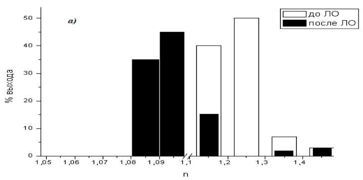
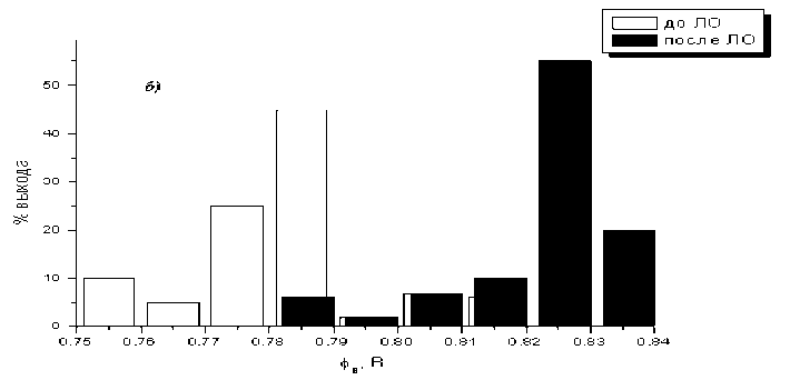
Fig. Distribution histograms of the ideality factor of Schottky diodes Pt-n-n+-GaAs before and after LA (a). Barrier height distribution histogram Schottky before and after LT (b), (λ=1.06 µm, τ=10ns, Р=3 □ 10-6 J/cm2)
At the same time, the dopant concentration calculated from the CV characteristics remained practically unchanged after laser exposure, which is in accordance with the experimental calculated data on the magnitude of the avalanche breakdown voltage of Schottky barriers, which for a concentration of ~1.1 □ 1016 cm-3 was 80 V. The reverse current of diode structures in the entire measured voltage range, up to the breakdown voltage, changed slightly after exposure to laser radiation, decreasing by a factor of 1.5– 2 with increasing radiation energy density. In this case, the capacitive cutoff voltage increased insignificantly. The noted changes in the parameters of Schottky barriers, as can be seen from the data presented, are observed at relatively low energy densities of laser radiation, at which phase transformations do not yet occur at the metalsemiconductor interface.
Measurements of the current-voltage characteristics carried out after a year of storage of the diode structures at room temperature showed that the parameters of the Schottky barriers on 100 diode cells formed on the n–n+ GaAs structure retained their parameters practically unchanged.
Thus, using laser irradiation of diode structures with a Schottky barrier on a GaAs wafer, by individually processing each diode, it is possible to obtain a high yield of diodes with identical Schottky barrier parameters.
References Effect of laser processing on the parameters of gallium arsenide Schottky diodes
- Джаманбалин К.К., Дмитриев А.Г. Эволюция барьерного контакта GaAs-Ni в омический при воздействии лазерного излучения. //ФТП. 1990. т.24. №11. с.2024-2028.
- Воронков В.П., Вяткин А.П., Иванов Б.В., Кулешов С.М., Рухадзе З.А. Вольтамперные характеристики контактов Pd-GaAs подвергнутых лазерному отжигу. //ФТП. 1989. т.23. №3 С.562-564.
- Бер Б.Я. Дайнова И.Р., Коробов В.А., Кулагина М.М., Прощепа Г.В., Пятаев В.З., Островский А.Ю., Этинбург М.М. Лазерное формирование омических контактов к арсениду галлия n-типа. //Письма в ЖТФ. 1991. т. 17. №20. С.74-79.
