Electronic structure of SnO 2 when doped with Sb and V

Author: Dobrosmislov Sergei S., Kirko Vladimir I., Nagibin Genadiy E., Popov Zahar I.
Journal: Журнал Сибирского федерального университета. Серия: Техника и технологии @technologies-sfu
Article in issue: 2 т.7, 2014.
Free access
There was carried out theoretical and experimental investigation of the influence of Sb and V dopes on the electrophysical properties of the SnO2-based ceramic materials. Modeling was done with the help of the program package VASP within the density functional formalism. The SnO2-based ceramics was synthesized according to the standard technology at the sintering temperature 1300 ºС with different Sb dope concentrations (1 to 5 %). The material made with V dopes had a low electrical conductivity. The structure investigation showed Sb being completely dissolved in the SnO2. The calculations showed that the activation energies are Egap(SbSn47O96)= 1.19 eV and Egap(VSn47O96)= 1.33 eV. The experimental investigation showed that the increase of the stibium oxide concentration leads to the decrease of the band-gap energy from 1.33 eV to 0.75 eV. The difference between the calculated activation energy value of the Sb-doped SnO2 and that obtained from the experiments is 19 %.
Ceramics, tin dioxide, electrical conductivity, voltage-current characteristic (vcc), energy-band structure, quantum-chemical modeling
Short address: https://sciup.org/146114829
IDR: 146114829 | UDC: 666.3
Электронная структура диоксида олова при легировании Sb и V
Проведены теоретические и экспериментальные исследования влияния легирующих добавок V и Sb на электрофизические свойства керамического материала на основе диоксида олова. Моделирование осуществлялось с использованием программного пакета VASP в рамках формализма функционала плотности. Керамика на основе диоксида олова синтезировалась по классической технологии при температуре спекания 1300 ºС, с различной концентрацией легирующих добавок сурьмы(от 1 до 5 % ). Материал, полученный при использование ванадия, обладал низкой электропроводностью. Исследование структуры показало полное растворение сурьмы в диоксиде олова. Проведенные расчеты показали, что энергия активации составляет Egap(SbSn47O96)= 1,19 эВ и Egap(VSn47O96)= 1,33 эВ. Экспериментальные исследования свидетельствуют о том, что увеличение концентрации оксида сурьмы приводит к снижению ширины запрещённой зоны с 1,33 до 0,75 eV. Различие между рассчитанным значением энергии активации диоксида олова, легированного сурьмой, и экспериментальными исследованиями составляет 19 %.
Text of the scientific article Electronic structure of SnO 2 when doped with Sb and V
The SnO2-based chemically resistant material of a high electrical conductivity is being widely used in many industries [1] – electronics, electrotechnology, electrochemistry, catalysis, biotechnology, metallurgy, atomic and chemical industries, etc. [2]. Pure tin dioxide is badly sintered that is caused by domination of the evaporation-condensation process over diffusion [3], as well as low conductivity associated with the high activation energy (4.3 eV). To improve sinterability glassforming dopes are used such as MnO 2 [4], CoO[5], CuO[6]. The investigations carried out formerly revealed that the ceramics obtained with the manganese (IV) and copper (II) oxides combination had the best physical-mechanical properties [7]. To improve electrophysical properties there are widely used Sb2O3[8] and V2O5[9]. While sintering the Sb and V dissolution in the SnO2 crystal lattice occurs [10].
However, the influence of the Sb and V atoms on the SnO2 electronic structure is not well investigated. The difficulty lies in the nonuniform ceramics structure because electrical conductivity is a function of the sintered material boundaries [11] and as a consequence depends on many factors such as the grain size, porosity, averagepore size, etc.
Modelling the energy-band structure and experimental investigation of the electrical physical properties will allow studying thoroughly the dope influence on the tin dioxide electronic structure.
The aim of the present paper is to investigate theoretically and experimentally the influence of Sb and V atoms on the electronic structure of tin dioxide in rutile phase.
Research technique
Structure modeling. All calculations are done within the density functional formalism (DFT) [12, 13] with the help of the program package VASP (Vienna Ab-initio Simulation Package) [14, 15]. The program above uses the pseudopotential method and expansion of the wave functionson plane wave basis. In the program to reduce a number of basic functions effectively and increase calculating speed Vanderbilt pseudopotentials are used for all atoms [16]. When optimizing the geometry all atoms’ coordinates in a supercell are variated by the conjugate gradient method with the usage of forces acting on atoms. The geometry optimization is being conducted until forces acting on every atom become lower than 0.05 eV/Å.
The synthesis technique. The furnace charge preparation → pressing the powder with 5 % polyvinylalcohol (PVA) → sintering at 1300 ºС.
For physical-mechanical tests the ceramic specimens were made in the form of cylinders 15 mm in diameter and of 10 mm height. For electrophysical measurements the specimens had the rectangular shape 5×4×50 mm.
The experimental technique. The investigation of physical-mechanical properties of the specimens was carried out according to the State Standards 24468-80, 530-95, 20419-83. The resistivity within the temperature range 20–1000 °С was measured with the four-point probe method [17]. To measure mechanical characteristics there was used the instrument Instron 3369. Phase composition, elements distribution and material structure will be identified by the X-ray phase analyzer XRD 6000 and electron microscope JEOL JSM-6490 LV.
Energy-band structure calculation
Tin dioxide is a semiconductor with the forbidden band energy 3.54 eV [18] and rutile crystal lattice structure.
Brillouin zones for the structure and calculated SnO 2 energy-band structure [19] are presented in Fig. 1.
There were calculated energy-band structures for supercells SbSn 47 O 96 and VSn 47 O 96 . When calculating the energy-band structure every direction in the reciprocal space was divided into 5 dots. Energy-band structure for SbSn 47 O 96 is presented in Fig. 2.
When doping SnO2 with V and Sb the activation energy decreases. At equal dope concentrations the band-gap energy, however, is greater by 0.14 eV when doping SnO 2 with vanadium atoms. The calculations carried out also showed that stibium as a dopant distorts the materials’ conduction levels much more. This may be caused by stronger interaction energy of stibium with tin dioxide.
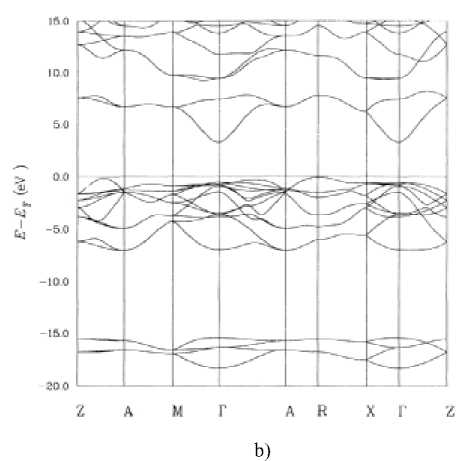
Fig. 1. (a) Brillouin zones for the rutile structure, (b) calculated SnO 2 energy-band structure
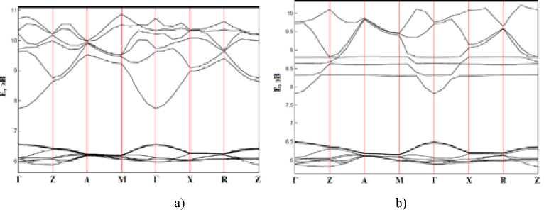
Fig. 2. Calculated energy-band structure: SbSn 47 O 96 (E fermi = 7.14 eV) E gap (SbSn 47 O 96 ) = 1.19 eV; VSn 47 O 96 (E fermi =
7.15 eV) E gap (VSn 47 O 96 ) = 1.33 eV
Experimental results
The vanadium oxide influences negatively on the physical-mechanical properties of SnO 2 . This may be caused by its poor solubility. Stibium oxide doesn’t have an influence on the properties. Most probably, a complete dissolution of stibium takes place in the SnO 2 crystallattice and the influence on the sinterability is absent.
The synthesized material structure
In case of the usage of MnO 2 – CuO dopes CuMnO x phase forms (mainly CuMn 2 O 4 , Cu 1.5 Mn 1.5 O 4 ) that is a glass phase on the grains’ boundaries and contributes to sintering [7]. A slight shift of the SnO2 crystal lattice picks witnesses the manganese oxide dissolution (Fig. 3).
Table 1. Physical-mechanical properties of the SnO 2 -based ceramics
|
№ |
Furnace charge composition |
Sintering temperature, ºС |
Density, kg/m3 |
Open porosity, % |
Strength, MPa |
Resistivity mOhm*m, T=1000 °C |
|
1 |
95 %SnO 2 -1 %Sb 2 O 3 - 2 %MnO 2 -2 %CuO |
1300 |
6121 |
1,77 |
432 |
0,28 |
|
2 |
94 %SnO 2 -2 %Sb2O 3 - 2 %MnO 2 -2 %CuO |
1300 |
6315 |
2,15 |
413 |
0,27 |
|
3 |
93 %SnO 2 -3 %Sb 2 O 3 - 2 %MnO 2 -2 %CuO |
1300 |
6215 |
2,42 |
399 |
0,24 |
|
4 |
92 %SnO 2 -4 %Sb 2 O 3 - 2 %MnO 2 -2 %CuO |
1300 |
6127 |
2,88 |
424 |
0,23 |
|
5 |
91 %SnO 2 -5 %Sb 2 O 3 - 2 %MnO 2 -2 %CuO |
1300 |
6206 |
4,84 |
401 |
0,2 |
|
6 |
94 %SnO 2 -2 %V 2 O 5 -2 %CuO |
1300 |
4621 |
28.4 |
51.9 |
- |
|
7 |
94 %SnO 2 -2 %V 2 O 5 -2 %MnO 2 |
1300 |
5389 |
16.4 |
192.7 |
- |
|
8 |
94 %SnO 2 -2 %V 2 O 5 -2 %AgO |
1300 |
5008 |
23.03 |
58.1 |
3,9 |
Electrophysical properties of the SnO2-based ceramics
The investigation of the electrophysical properties of the material with the V 2 O 5 dope revealed that at temperatures about 1000 ºС electrical resistance remains high. This means either that the vanadium solubility in the SnO 2 crystal structure is low, or the binding energy V – O is high.
For semiconductors there is characteristic an exponential relationship between the resistivity and temperature [20]:
ρ = ρ 0 ∙ exp( E a /2 kT ), (3)
where ρ0 – an initial electrical resistivity, Ohm*m; Ea – the band-gap energy, J; k – the Boltzmann constant; T – temperature.
|
^ Ду - W i Г' г, г ^А.Ь- \ ^^ ^J»^ еу^, * №, 4 А* ViTZLieV ^ »Л-" >’ Z Г Л зДг* /• > / «" . г . г 2- * * •, . * ,\ |
Spectrum |
0 |
Ж |
|
|
Spectrum 1 |
75.13 |
0.56 |
24.3 i |
|
|
Spectrum 2 |
69.03 |
0 |
30.97 |
|
|
Spectrut 3 \ |
53.40 |
0.75 |
40.35 |
|
|
Spectrum 4 |
77.06 |
0 |
22.94 |
|
|
Spectrum 5 |
76.30 |
0 |
23.70 |
|
|
ma^ |
77.06 |
0.75 |
40.85 |
|
|
min. |
58.40 |
0.56 |
22.94 |
Fig. 4. Raster electron microscopyphotography of the 94 %SnO 2 -2 %Sb 2 O 3 -2 %CuO-2 %MnO 2 ceramics (JEOL JSM-6490 LV), x500
The resistivity measurement results for the ceramic material with different stibium oxide concentrations are presented in Fig. 5.
In Fig. 5b there are presented the resistivity measurement results for the ceramic materials with different stibium oxide concentrations in the logarithmic coordinate.
As follows from the experimental results, an increase of the stibium oxide concentration leads to the band-gap energy decrease from 1.33 eV to 0.75 eV.
When increasing the stibium oxide concentration up to 5 % there takes place a qualitative change of the VCC curve shape. This may be associated with a partial and chaotic Sb atoms dissolution in the SnO 2 crystal lattice.
Conclusions
Theoretical investigation showed that at equal V or Sb dope concentrations the band-gap energy is greater by 0.14 eV when doping SnO 2 with vanadium atoms.
Table 2. The ceramic materials’ activation energy
|
Composition |
95 %SnO 2 -1 %Sb 2 O 3 -2 %MnO 2 -2 %CuO |
94 %SnO 2 - 2 %Sb2O 3 - 2 %MnO 2 - 2 %CuO |
93 %SnO 2 -3 %Sb 2 O 3 -2 %MnO 2 -2 %CuO |
92 %SnO 2 -4 %Sb 2 O 3 -2 %MnO 2 -2 %CuO |
91 %SnO 2 -5 %Sb 2 O 3 -2 %MnO 2 -2 %CuO |
|
Е Act , eV |
1.33 |
1.33 |
1 |
1 |
0.75 |
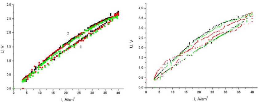
Fig. 6. Voltage-current characteristics (VCCs) of the specimens at threefold measurement (Т=1000ºС): 1 – Current strength increasing; 2 -Current strength decreasing: (а) 94 %SnO 2 -2 %Sb 2 O 3 -2 %CuO-2 %MnO 2 (б) 91 %SnO 2 -5 %Sb 2 O 3 -2 %CuO-2 %MnO 2
The difference between the calculated Sb-doped SnO 2 activation energy and that obtained from the experiments is 19 % that in case of ceramics is satisfactory.
The V-doped material made according to the standard ceramic technology has a low electrical conductivity. This may be associated with a poor solubility of vanadium in the tin dioxide and requires a change of the synthesis technique.
The experimental investigation showed that the increase of the stibium oxide concentration leads to the decrease of the band-gap energy from 1.33 eV to 0.75 eV.
The reported study was partially supported by RFBR, research project No. 14-02-31309.
