Enhancing Leakage Power in CPU Cache Using Inverted Architecture

Author: Bilal A. Shehada, Ahmed M. Serdah, Aiman Abu Samra
Journal: International Journal of Modern Education and Computer Science (IJMECS) @ijmecs
Article in issue: 2 vol.5, 2013.
Free access
Power consumption is an increasingly pressing problem in modern processor design. Since the on-chip caches usually consume a significant amount of power so power and energy consumption parameters have become one of the most important design constraint. It is one of the most attractive targets for power reduction. This paper presents an approach to enhance the dynamic power consumption of CPU cache using inverted cache architecture. Our assumption tries to reduce dynamic write power dissipation based on number of ones and zeros in the in-coming cache block data using bit to indicate is the block is mostly one or zero. This architecture reduces the dynamic write power by 17 %. We use Proteus Simulator to test that proposed circuit and performed the experiments on a modified version of the cacti6.0 simulator.
SRAM, Cache, Inverter, Dynamic power, Static power, CMOS
Short address: https://sciup.org/15014518
IDR: 15014518
Text of the scientific article Enhancing Leakage Power in CPU Cache Using Inverted Architecture
Published Online February 2013 in MECS
Modern microprocessors employ on-chip caches. This is due to the fact that caches can significantly reduce the speed gap between processor and main memory. For high speed clock frequency, the on-chip caches are usually implemented using packed static random access memory (SRAM) cells. The numbers of transistor of these caches are increasing resulting an increaseing in the power consumption.
-
A. Satatic and Daynamic Power
Electrical power can be defined as the product of the electrical current thro ugh times th e voltage at the terminals of a power consumer. The static power (Pstatic) is dissipated due to leakage currents amounts to less than 5% of the total power dissipated at 0.25μm. It has beenobserved that the leakage power increases by about a factor of 7.5 for each technological generation and is expected to account for a significant portion of the total power in deep sub-micron technologies [1]. Therefore, the leakage power component grows to 20-25% at 130 nm [2]. The dynamic component Pdynamic of the total power is dissipated during the switching between logic levels, due to charging and discharging of the capacitance, and due to a small short circuit current. For example, when the input signals for the CMOS inverter switches from one level logic level to the opposite, then there will be a short instance when both the pMOS and nMOS transistors are open. During that time instant a small short circuit current Isc flows from Vdd to Gnd. Short circuit power can consume up to 30% of the total power budget if the circuit is active and the transition times of the transistors are substantially long. However, through a careful design to transition edges, the short circuit power component can be kept below 10-15% [3]. In CMOS circuits, this component accounts for 70-90% of the total power dissipation [3].
In recent years the heat that resulted from power consumption in cache due to dynamic power caused by transactions in SRAM cache restricts the development of cache. Froe example the DEC21164 dissipates 25% and the StrongArm- 110 dissipates 42% of its total power in caches. Moreover, the power consumption for the new emerging nano-scale technology is getting worse. The decrease of threshold voltage affects negatively leakage, i.e., static power, and hence the total power consumption. For this reason, numerous techniques have been proposed to reduce cache memory power. The techniques target both dynamic power and static power consumption.
-
B. Power Consumption Trends In Integrated Circuits
Power provides challenges as processors are scaled and power must be brought in and distributed around the chip, while modern processors use hundreds of pins and multiple interconnect layers for just power and ground and power is wasted as heat and must be reduced. Increase in the number of transistors switching, and the frequency with which they switch, dominates the decrease in load capacitance and voltage, leading to an overall growth in power consumption and energy [4].The earlier microprocessors consumed tenths of a watt, while a 3.2 GHz Pentium 4 Extreme Edition consumes 135 watts. The distribution of energy, heat removal and avoiding hot spots have become increasingly difficult challenges. in the past it was raw silicon area but with modern technology power is now the major limitation to using transistors. Today most of the microprocessors turn off the clock of inactive modules to save energy and dynamic power but Increasing the number of transistors increases power even if they are turned off, and leakage current increases in processors with smaller transistor sizes.
Caches are used to keep the most frequently used data readily available and easily accessible, increasing overall application performance. In the world of memory hierarchy[], a rule of thumb of relative access cost is summarized in this table:
TABLE I: summarize relative access cost for each type of RAM
|
Relative Latency |
Memory System Level |
|
1x |
L1 Cache |
|
10x |
Higher Cache Levels |
|
100x |
Main Memory |
What this means is that using data already in a Level 1 (L1) cache is 100 times faster than fetching the data from the main memory.
Important to realize that performance optimizations can be very specific they depend on the exact architecture of the machine (processor, memory, etc), the exact version of the compiler, the exact version of the operating system and the particular configuration of the program that we are trying to optimize.
The rest of the paper is organized as follows: related work is discussed in Section II. In Section III .describe SRAM Cell Design .In Section IV, we describe the design and implementation. In next section, V Simulation and Experiments Finally, conclusions are presented in the last section.
-
II. RELATED WORK
Many papers are introduced to reduce cache power including Low Power Cache Architecture [5] the idea is to separate Cache into two banks one which stores, mostly data that contains more zeros and the other bank stores data that have mostly Is in its contents. This separation aims to reduce switching activity when replacing data in c ac h e lines. The paper shows up to 35% power reduction for small sized caches and about 6-10% for medium sized caches. However, this paper has a problem in cache size, which is halving or doubling witch in the first case increase the miss rate and in the second case increase, the cost and one of the major problems it is increasing of the miss rate.
A Variable Bitline Data Cache for low power design [5] proposes a Variable Bitline Data Cache (VBDC) which exploits the popularity of NWV stored in the cache. In VBDC design, the cache data array is divided into several sub-arrays to adapt each data pattern with the different bitline length to access. The VBDC can shut off the corresponding unused high arrays to reduce its dynamic and static power consumption. The VBDC achieves low power consumption through reducing the bitline length.
Low power cache architecture with security mechanism [7] presents a novel easily implemented cache architecture which has an added small cache and adopts certain operation mechanism. Compared with traditional cache archi t ectur e , it has reduction in miss rate ranging between 20% and 50%, and has about 8.5% of reduction in power consumption, and is secure at the same time. This paper presents both theoretical analysis and experimental results.
Frequent V a l u e D a t a C a c h e [8] the idea of this paper is how this frequent value phenomenon can be exploited in designing a cache that trades off performance with energy efficiency. It proposed the design of the Frequent Value Cache (FVC) in which storing a frequent value requires few bits as they are stored in the encoded form while all other values are stored in the uuencoded form using 32 bits. The data array is partitioned into two arrays such that if a frequent value is accessed only the first data array is accessed; otherwise an additional cycle is needed to access the second data array.
Low power architecture cache for embedded systems [9]introduce a novel low power cache architecture for embedded system based on low power architecture with modification the idea is to separate cache associatively into two banks mostly zero and mostly ones for reduce cache miss.
Dynamic Zero Compression for Cache Energy Reduction introduce a novel technique for cache [10] energy reduction, dynamic zero compression (DZC), which exploits the prevalence of zero bytes stored in the cache. DZC adds an additional zero indicator bit (ZIB) to each cache byte that indicates whether the byte contains all zero bits.
Saving register-file static power by monitoring instruction sequence in ROB [11] introduce a monitoring mechanism is built in the ROB and the register file to identify the timing of usage for each register. This mechanism can be integrated with a DVS approach on the datapath to power down (or up) the supply voltages to a register when it is idle (or active).
A leakage-aware L2 cache management technique for producer–consumer sharing in low-power chip multiprocessors [12] proposes a novel leakage management technique for applications with producer– consumer sharing patterns. By exploiting particular access sequences observed in producer–consumer sharing patterns and the spatial locality of shared buffers, our technique enables a more aggressive turnoff of L2 cache blocks of these buffers.
On the design of low-power cache memories for homogeneous multi-core processors [13] investigate the impact of level-1 cache (CL1) parameters, level-2 cache (CL2) parameters, and cache organizations on the power consumption and performance of multi-core systems. We simulate two 4-core architectures - both with private CL1s, but one with shared CL2 and the other one with private CL2s.
-
III. SRAM CELL DESIGN
Static random access memory (SRAM) has been widely used as the representative memory for logic LSIs.
This is because SRAM array operates fast as logic circuits operate, and consumes a little power at standby mode. Another advantage of SRAM cell is that it is fabricated by same process as logic, so that it does not need extra process cost. These features of SRAM cannot be attained by the other memories such as DRAM and Flash memories. SRAM memory cell array normally occupies around 40% of logic LSI nowadays, so that the nature of logic LSI such as operating speed, power, supply voltage, and chip size is limited by the characteristics of SRAM memory array.
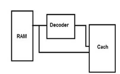
Fig.1 proposed inverted rchitecture
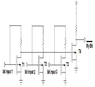
Fig.2 decoder Circuit
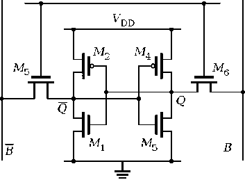
Fig.3 SRAM Circuit
Therefore, the good design of SRAM cell and SRAM cell array is inevitable to obtain high performance, low power, low cost, and reliable logic LSI. An SRAM cell is the key SRAM component storing binary information. A typical SRAM cell uses two cross-coupled inverters forming a latch and access transistors. Access transistors enable access to the cell during read and write operations and provide cell isolation during the not-accessed state. An SRAM cell is designed to provide non-destructive read access, write capability and data storage for as long as cell is powered [13]. A 6T CMOS SRAM cell is the most popular SRAM cell due to its superior robustness, low power and low-voltage operation.
Power consumption in a digital integrated circuit is governed by using (1):
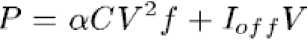
Where α is the average switching activity factor of the transistors, C is capacitance, V is the power supply voltage, f is the clock frequency, and Ioff is the leakage current. The first term of the equation is dynamic power and the second term is static power.
-
A. SRAM Read Operation
In the 6-transistor circuit depicted in Fig.3 during the read operation, one node of the RAM cell pulls the bit line up through the access transistor and the PFET-load and another node pulls the bit line down through the pass transistor and NFET load.
During a read operation both bit lines (BL and BL bar) are pre-charged to V DD . The word line (W) is initially help low. Assume “1 “i s stored at the Q. If the word line transitions high, it enables both transistors M5 and M6. Transistors M3 and M2 are “OFF” while M1 and M4 are “ON”.
-
B. SRAM Write Operation
When the word line is selected, Q5and Q6 is on and the level stored in Q5 and Q6 are passed to the bit lines. Logic “1” when Q1 is off andQ2is on, Q5is at Vdd, C6is at Vss. Logic “0”vwhen Q3vis off and Q4 is on, Q5 is at Vss, Q6 is at V dd .
-
C. Static Noise Margin of SRAM Cells
NMH =VOH –VIH (2)
NML =VIL-VOL (3)
where VIL is the maximum input voltage level recognized as logical “0”, VIH is the minimum input voltage level recognized as a logical “1”, VOL is the maximum logical “0” output voltage, VOH is the minimum logical “1” output voltage. One important index to evaluate an electrical stability is static noise margin (SNM). This index represents the margin voltage in which data upset occurs during read operation. To estimate the SNM, the word line and a pair of bit lines are connected to VDD shown in Fig. 4.
The SNM is simulated as follows:
-
1. While raising the N0 voltage from 0 V to VDD, measure the N1 voltage and N1–N0 relations are plotted.
-
2. While raising the N1 voltage from 0 V to
-
3. VDD, measure the N0 voltage and N0–N1 relations are plotted.
-
4. Draw squares as large as possible between the line
A and the line B (Squares C and D).
-
1. A length of diagonal line of the smaller square is designed as the SNM.
These A and B lines are called as a “butterfly curb.” In Fig. 5, the butterfly curbs are shown at VDD D 0:6V and 1.1V. An SRAM cell provides a smaller noise margin at lower voltage. The asymmetry of butterfly curbs increases as the threshold voltage (Vth) variation in a cell increases. As a result, the SNM decreases.
Lower Vth of driver MOSFET decreases the SNM. The ratio of the gate width of driver MOS to that of an access MOS is called ˇ ratio. Larger ˇ ratio increases the SNM. This is because the N0 voltage rise by _VN can be restrained by increasing the driver MOS current and decreasing the access MOS current. Generally, in the SRAM cell, the ˇ ratio is over 1.5.
Because the full CMOS 6-T memory cell statically retains data, it does not need special treatment like refresh. At read operation, fast access time is achieved because complementary bit line signals make it possible to use differential amplifier. Therefore, SRAM is used as cache memory.
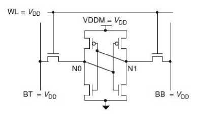
Fig. 4. Connections of the word line and a pair of bit lines to estimate the SNM
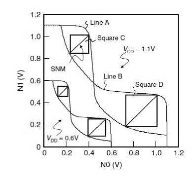
Fig.5. Butterfly curbs are shown at VDD D 0:6V and V
-
IV. PROPOSED DESIGN AND IMPLEMENTATION
Leakage power consumption becomes a major design issue in realizing low-power microprocessors as the process technology advances. We introduce a novel low power on- chip cache Architecture, which reduces dynamic power dissipation in the Cache. Our design is based on low power architecture [1] with modification.
By assuming that all data that will enter to the cache must be mostly zeroes so if data is mostly ones we try to invert it and add one flag bit in the cache to indicate that data is inverted.
We attach new bit we named it, invert bit flag this bit calculated before new data added to the cache when cache miss or cache write occurs, and they have value 0 if the data mostly zeros or 1 if the data stream is mostly ones means that the data must be inverted. this value is calculated using comparator (or simple decoder) witch have data bus input and only one bit output as shown in fig.1 .The comparator circuits not exceed than hundreds transistor and today s cache circuit contain millions of a transistor so the power effected of this comparator is approximate nothing compared with the total power of cache .
We can use fig.1 to classify data mostly ones or mostly zeros. Our design depends on voltage divider concept. We connect the v dd of the transistor to the input and connect all of the output to a transistor of the input to this transistor is enough to operate it then the data is mostly zeros if not data is mostly ones. For example if we have 3 input data 110 then T1 and T2 will operate T3 will not operate the input of T4 is enough to operate it the output of T4 (my_bit ) is 0 that s means the data input is mostly ones.
We know that there is no power consumption in inverting operation because we have data and inverted data in the same sram cell. Memory core is composed of memory cells that are arranged in rows and columns. Fig. 2 shows the typical 6- transistor memory cell design.
In our design as shown in fig. 6, we enhance SRAM cell by adding 2 transistors (M7 & M8) one at the end of Data (M7) and other to Data' (M8) and connect its V DD to inverted bit and inverted bit' respectively. When data input is 1 and inverted bit is 0 then M7 be OFF and M8 ON then data out will be 1 (B"=B), data input is 1 and inverted bit is 1 then M7 be ON and M8 OFF then data out will be 0, data input is 0 and inverted bit is 0 then M7 be OFF and M8 ON then data out will be 0 ,data input is 0 and inverted bit is 1 then M7 be ON and M8 OFF then data out will be 1 as shown in table1. Fig.7 a. shows an example using typical model of SRAM cache and Fig.7.b shows our enhancement.
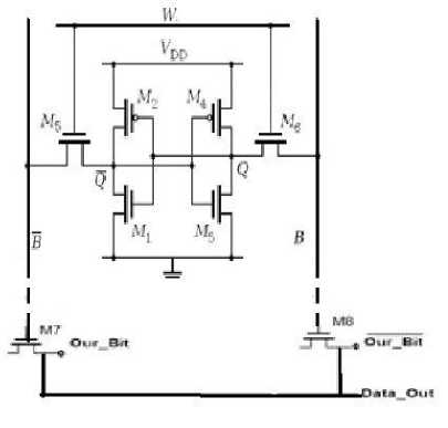
Fig.6 proposed circuit design
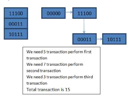
Fig.7. a example shows number of transaction in typical SRAM
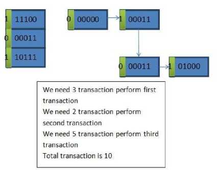
Fig.7. b example shows number of transaction in proposed SRAM
Table II: output bits
|
out |
Data |
Inverted_Bit |
|
0 |
0 |
0 |
|
1 |
1 |
0 |
|
1 |
0 |
1 |
|
0 |
1 |
1 |
In our design we assume that block size divided into 8 part each part has its own inverted bit indicator.
-
V. SIMULATION AND EXPERIMENTS
We evaluate the effectiveness of the proposed approach. We use proteus simulator to test that our circuit and we performed our experiments on a modified version of the cacti6.0 [14] simulator using four threads. In our experiment we use 64 byte block size (512 bit ), we divide the block size into 8 parts, each part has its own inverted bit, actually the overhead of our design is 1/64 (1.5625%), with changing cache size, set of Associative is 2 and technology 32 nanometer and obtain the result as shown in Fig.8. In other experiment steps we use 64 byte block size (512 bit ), we divide the block size into 8 parts, each part has its own inverted bit, actually the overhead of our design is 1/64 (1.5625%), with changing set of Associative, cache size 64kbyte- and technology 32 nanometer and obtain the result as shown in Fig.9.
-
VI. CONCLUSION
In this paper, we proposed an inverted low power cache architecture which reduces dynamic write power dissipation based on number of ones and zeros in the in- coming cache block data using bit to indicate is the block is mostly one or zero. The architecture reduces the dynamic write power by 17 % and this value increase if the block size decreased.
Power consumption in mW
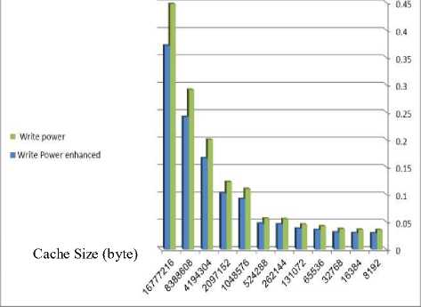
Fig.8 . simulation result using 64 byte block size, set of Associative is 2 and technology 32 nanometer
■ Write power
■ Write Power enchanced
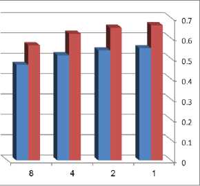
Fig.9. simulatio n result using 64 byte block size and technology 32 nanometer
References Enhancing Leakage Power in CPU Cache Using Inverted Architecture
- S. Borkar, Design Challenges of Technology Scaling, IEEE Micro, 19(4):23–29, 1999.
- R. Aitken, G. Kuo, and E. Wan, Low-Power Flow Enable Multi-Supply Voltage ICs, EETimes, http://www.eetimes.com/news/design/show Article. 2005.
- J. Hennessy, D. Patterson, Computer Architecture A Quantitative Approach, Fourth edition, 2007.
- J. M. Rabaey, A. Chandrakasan, and B. Nikolic, Digital Integrated Circuits. Pearson Education International, 2 edition, 2003 , London u.a.
- M. Nakkar and N. Ahmed, Low Power Cache Architecture, Int System on Chip for Real Time Applications, IEEE, 2006.
- Y. Jiongyao, T. Watanabe, A Variable Bitline Data Cache for low power design, Microelectronics and Electronics (PrimeAsia), Asia Pacific Conference on Postgraduate Research in, 2010.
- Ch. Li, F. Qiao, H. Yang, Low power cache architecture with security mechanism, Education Technology and Computer (ICETC), 2nd International Conference on, 2010.
- J. Yang and R. Gupta, Energy Efficient Frequent Value Data Cache Design, Int. Symp. On Microarchitecture, Nov, 2002.
- A. Abu Samraa , A. Alsalhi and R. Abutair, Low Power Architecture Cache For Embedded Systems, Alazhar University journal 2010.
- L. Villa, M. Zhang and K. Asanovi´c, Dynamic Zero Compression for Cache Energy Reduction, 33rd International Symposium on Microarchitecture, Monterey, CA, December 2000.
- W. Shieh, H. Chen , Saving Register- File Static Power By Monitoring Instruction Sequence In ROB, Journal of Systems Architecture 57, 2011.
- H. Kim, J. Kim, A Leakage- Aware L2 Cache Management Technique For Producer–Consumer Sharing In Low-Power Chip Multiprocessors, J. Parallel Distrib. Comput. 71, 2011.
- A. Pavlov, M. Sachdev, CMOS SRAM Circuit Design and Parametric Test in Nano-Scaled Technologies.
- http://www.hpl.hp.com/research/cacti/.
- A. Asaduzzaman, M. Rani, F.N. Sibai, On The Design Of Low-Power Cache Memories For Homogeneous Multi-Core Processors Microelectronics (ICM), International Conference, 2010.
- K. Bhattacharya, S. Kim and N. Ranganathan Improving the Reliability of On-chip L2 Cache Using Redundancy, Computer Design, ICCD 2007, 25th International Conference, 2007.
