Fault Tolerant ALU using Parity Preserving Reversible Logic Gates

Author: Shaveta Thakral, Dipali Bansal
Journal: International Journal of Modern Education and Computer Science (IJMECS) @ijmecs
Article in issue: 8 vol.8, 2016.
Free access
Demand of reliable computing has been a major concern since the dawn of the electronic digital computer age. Reliable computing has various applications not only in the field of military, aerospace and communication but even contemporary commercial applications to fulfill today's automated life style. The tremendous growth in fabrication from small scale integration (SSI) to giant scale integration (GSI) is facing power dissipation as one of the main barriers. To overcome this barrier, researchers need to enter into the reversible logic domain. Making a reversible circuit robust or fault tolerant is much more difficult than a conventional logic circuit. Fault tolerance can be achieved in a system by using parity bits. The main aim of this paper is to come up with a new fault tolerant ALU design based on parity preserving reversible logic gates with improved quantum cost and power overhead as compare to existing fault tolerance based ALU designs. The most stringent requirement for fault tolerant ALU is in real time control system where faulty computation jeopardizes human life or other catastrophic effects.Implentation of proposed design is done using Xilinx ISE design suit 14.2 tool and its performance over existing ALU designs is qualitatively analyzed.
ALU, Fault tolerant, Power Dissipation, GSI, Quantum Cost, Reliable computing
Short address: https://sciup.org/15014894
IDR: 15014894
Text of the scientific article Fault Tolerant ALU using Parity Preserving Reversible Logic Gates
Published Online August 2016 in MECS DOI: 10.5815/ijmecs.2016.08.07
-
I. Introduction
In 1961, Landauer [1] stated that “amount of energy dissipated for every bit erasure during an irreversible operation is given by KTln2 joules where K is Boltzman’s constant and T is the operating temperature. In 1973, Bennett [2] proposed the solution to R. Landauer statement and showed that KTln2 energy dissipation would not occur, if computation is done in a reversible manner since amount of energy dissipated in a system depends directly on numbers of bits erased during computation. Classical gates like two input AND, OR, NAND, NOR, XOR and XNOR are irreversible as we can't uniquely reconstruct input states from output states. Here two-bit input state is mapped to one-bit output state
leads to the erasure of one bit and consequently loss of energy. We can avoid this energy loss by mapping n bit input states to n bit output states so that input states can be uniquely recovered from output states and under such circumstances, a gate is said to be reversible. The number of inputs in a reversible logic circuit should be equal to number of outputs and fan out is not allowed.
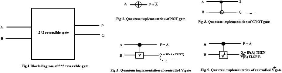
The quantum cost of a reversible gate is total number of 1x1 and 2x2 reversible gates required in the design. The quantum costs of all reversible 1x1, as well as 2x2 gates, are taken as one. Since every reversible gate consists of various 1 x 1 or 2 x 2 quantum gates are taken from NCV gate library containing combinations of NOT, CNOT and controlled V and controlled V+ gates, therefore the quantum cost of a reversible gate can be calculated by counting the numbers of NOT, Controlled-V, Controlled-V+ and CNOT gates. Integrated qubit gates are also used in the quantum implementation of reversible logic gates. Integrated qubits are a combination of Feynman gate and either controlled V or controlled V+ gate. Quantum cost of integrated qubit gate is also one Quantum cost for any reversible logic circuit should be as low as possible. As NCV gate library contains following set of quantum gates i.e. NOT gate, CNOT gate and controlled V and controlled V+ gates. Controlled V and controlled V+ gates are basically types of controlled square root of NOT gates. In both of these gates, when control input is 0 then second input is propagated as it is to output, Two V gates in series operation becomes CNOT gate or inverter. Similarly two V+ gates activated in series operation becomes CNOT or inverter gate and one V and another V+ gate in series operation become an Identity gate or buffer. Here block diagram of a 2*2 reversible gate is presented in Fig.1 with A and B as input and P and Q as output. Here quantum implementation of NOT gate, CNOT gate and Controlled V and controlled V+ gates is given in Fig.2, Fig.3, Fig.4 and Fig.5 respectively .Quantum implementation of integrated qubit gates can be implemented by cascading quantum implementation of CNOT gate with controlled V gate or with controlled V+ gate.
0 = Аф В
Q = IF(A) THEN V(B)ELSEB
-
II. Background on Fault Tolerance
Reliability is a major concern in reversible computing. Although reversible circuits are information lossless; they can recover bit loss occurring in the system but they are not able to detect bit error in the system. Hence fault tolerant reversible systems need to be developed to achieve robustness and reliable systems which are highly demanded by ultra low power integrated circuits.
-
A. Fault Tolerance Reversible Systems
A fault in a system is some deviation from the expected behavior of the system leads to malfunctionality. Faults may occur due to a variety of factors, including hardware failure, software failure, bugs, operator or user error, and some other network problems. Fault tolerant system continues to operate satisfactorily even in the presence of faults [3]. A fault-tolerant system may be able to tolerate one or more fault-types including -transient software and hardware design errors, operator errors or any other physical damage.
Aim of this paper is to incorporate fault tolerance property into ALU design using parity preserving reversible logic gates. It will not only reduce hardware overhead but also avoid extra design efforts for introducing fault tolerant system Parity preserving reversible logic gates are also called as conservative reversible logic gates or fault tolerant gates.
-
B. Parity Preserving and Conservative Reversible Logic Gates
Parity checking is one of the methods for error detection in digital logic system. In parity preserving reversible circuit, parity preserving reversible logic gates [4] are used in which parity if input vector must match parity of output vector. A reversible circuit will be parity preserving if its individual gate is parity preserving. As parity preserving reversible logic gates used between fault side and output are information lossless. Hence an error at fault side will be immediately seen at output. Parity preserving reversible gates allows detecting such faults at output which won’t affect more than a single logical signal. Conservative logic gates exhibit property that there are equal numbers of 1’s in output as there are in input. Every conservative gate is parity preserving but every parity preserving gate is not conservative.
There are many parity preserving logic gates reported in literature. Among them are Fredkin gate with quantum cost of 5, double Feynman gate with quantum cost of 2, NFT gate and MNFT gate with quantum cost of 7, Islam gate [5] and modified Islam gate (MIG) with quantum cost of 7, Five variables parity preserving gate (F2PG) with quantum cost of 14.Other gates found in literature are PPHCG, PCMF (Parity conserving multifunctional) and PPPG gate. It has been found that among existing 24 2*2 reversible logic gates, only 4 are parity preserving and among them only 2 are conservative. Similarly among existing 40320 3*3 reversible logic gates, only 576 are parity preserving and among them only 36 are conservative. Only Fredkin gate and PCMF are parity preserving as well as conservative. Others are parity preserving but not conservative. Quantum implementation of Fredkin gate, double Feynman gate, MNFT gate, MIG gate and F2PG gate is given in Fig.6 to Fig.10 respectively.
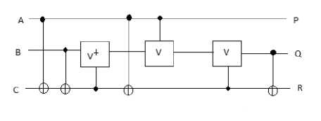
Fig.6. Quantum implementation of fredkin gate
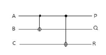
Fig.7. Quantum implementation of double feynman gate (DFG)
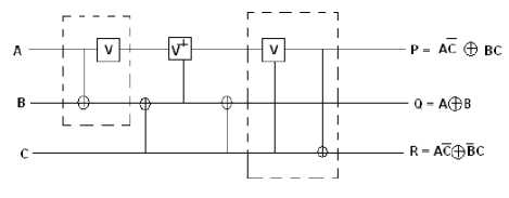
Fig.8.Quantum implementation of MNFT gate
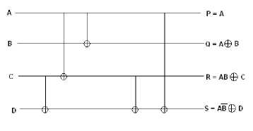
Fig.10.Quantum implementation of F2PG gate
-
III. Related Work
-
A. Arithmetic and Logical Unit
ALU is a data processing unit, which is an important part in CPU. Different kinds of computers have different ALUs. In logical operations, there are NOT, OR, AND, XOR, etc. while in arithmetic operations there are addition, subtraction, etc. For generating a reversible ALU, each of these general elements, as shown in Fig.11, is buildup with the help of reversible logic. The several sub-modules in the design are adder like BCD adder, Multiplier, and a logical unit. All the operations are done simultaneously. Depending on the control signal, the needed result is offered at the output.
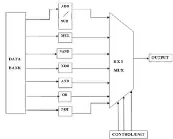
Fig.11. Block diagram of ALU
After a detailed analysis of the various designs of ALU, It has been concluded that each ALU could be divided on following two parameters based on their design.
-
1. Dedicated Design
-
2. Control Unit with Adder
In the similar fashion these ALUs are also divided into further two categories, named as:
-
1. Single line output
-
2. Multi line output
So all the possible categories of various ALU designs are summarized in Table 1.
Table 1. Categories of Various ALU Designs
|
Design Structure/Number of Output Lines |
Single Line Output |
Multi Lines Output |
|
Dedicated Design |
Design 1,2,3 |
Design 5 |
|
Control Circuit based Design |
Design 4 |
Not existing |
-
B. Existing ALU Designs
Existing ALU designs with their proposed methodologies are given below:
Design1. Matthew et al.[6] proposed a novel 5*5 reversible logic gate popular as MG i.e. Morrison gate that is used in designing of a novel reversible ALU along with HNG gate . Reversible ALU designed with MG and HNG gates performs arithmetic operations such as addition and subtraction and logical operations as AND, OR, NAND, NOR, XOR, and buffer. After that, the comparison heading towards the flowing factors such as the ripple-carry, carry-select, logged stone carry-ahead adders is being observed. Fig 12 shows here with proposed methodology.
Fig.12. Reversible ALU with MG and HNG gates
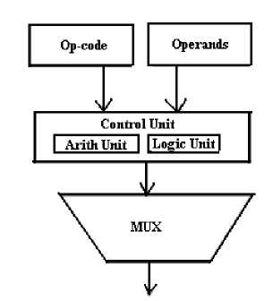
Fig.13. Reversible ALU based on control circuit
Design 2 and Design3.Syamala and Tilak [7] have proposed two approaches of ALU design i.e. control structure based reversible one-bit ALU and multiplexer based reversible one-bit ALU with further two types. Type 1 reversible one-bit ALU designing is done by using Peres gate, Feynman Gate, and Fredkin gate and Type 2 reversible one-bit ALU designing is done by Feynman gate, Fredkin gate, Peres gate, DPG gate and YAG gate. Control structure based reversible one-bit ALU designing is done by combinations of Toffoli, Feynman, and Fredkin gates. Control structure based ALU has been found to be complex to design due to various controls and slow in operation because of larger logic depth simultaneously with benefits of smaller logic width and less number of constant inputs. Fig 13 shows here with proposed methodology.
Design 4. Zhijin et al. [8] proposed ALU design which consists of two main parts i.e. reversible function generator as control unit and reversible mode selection unit. These two parts are cascaded by combinations of Toffoli and NOT gates. Arithmetic and logical operations performed by this ALU are addition, subtraction, inversion, NOR, NAND, XOR, XNOR, AND, OR, Buffer. Fig 14 shows here with proposed methodology.
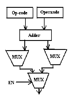
Fig.14. Multiplexer based reversible one-bit ALU
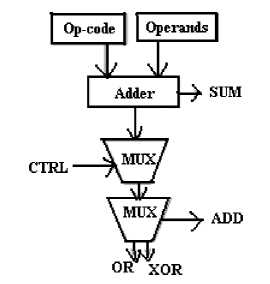
Fig.15. Dedicated design with Multi output
Design 5. Ravi et al. [9] discussed realization of with the help of a carry save adder block which are not based on propagation of carry bits. This approach results in improved of 20% and 17% regarding the gate count and quantum cost respectively, while comparing with earlier works in reversible ALU designs. This design has a dedicated unit for the logical and the arithmetic operations, which is a combination of Carry save adder,
Fredkin, Toffoli and CNOT reversible logic gates. But having the multiple outputs, to make this ALU functional more gates need to be added so that it can be implemented logically. Fig 15 shows here with proposed methodology.
The most stringent requirement for fault tolerant ALU is in real time control system where faulty computation jeopardizes human life or other catastrophic effects [10]. Section IV describes methodology for proposed fault tolerant ALU. Section V describes comparison and results. Section VI describes conclusion.
-
IV. Proposed Fault Tolerant Alu
The proposed ALU consist of the control unit and the reversible adder circuit. The control unit computes the function, input to the adder circuit, using which the output function is calculated. ALU is constituted of the Fredkin, double Feynman and NFT which are parity preserving gates, will hold the parity for the complete operation, this provides the ALU to function smoothly in harsh conditions and the output given by the system can be trusted as it will be verified using the parity.The proposed Fault tolerant Reversible 1- bit ALU is configured to perform 5 logical and 7 arithmetic operations as shown in Table 2 and 3 respectively.
Table 2. Function Table for Logical Operations
|
S 0 |
S 1 |
S 2 |
C |
Output |
Function |
|
0 |
0 |
1 |
x |
A+B |
OR |
|
1 |
0 |
1 |
x |
A.B |
AND |
|
0 |
1 |
1 |
x |
АфВ |
XOR |
|
1 |
1 |
1 |
x |
A' |
NOT |
|
1 |
1 |
0 |
1 |
A |
Transfer A |
Arithmetic and logical operations performed by this ALU are addition, subtraction, increment, inversion, XOR, AND, OR, Buffer.
Table 3. Function Table for Arithmetic Operations
|
S 0 |
S 1 |
S 2 |
C |
Output |
Function |
|
0 |
0 |
0 |
0 |
A |
Transfer A |
|
0 |
0 |
0 |
1 |
A+1 |
Increment A |
|
1 |
0 |
0 |
0 |
A+B |
Addition |
|
1 |
0 |
0 |
1 |
A+B+1 |
Add with Carry |
|
0 |
1 |
0 |
0 |
A+B' |
Subtract with Borrow |
|
0 |
1 |
0 |
1 |
A+B'+1 |
Subtraction |
|
1 |
1 |
0 |
0 |
A-1 |
Decrement A |
Proposed fault tolerant ALU circuit comprises of one NFT gate, two double Feynman gates and three Fredkin gates which are parity preserving reversible logic gates and one HNG gate. Proposed circuit in total consists of 7 reversible logic gates and quantum cost of circuit is 30.There are six ancillary inputs and six garbage outputs which need to be added to maintain reversibility. Power consumed by proposed fault tolerant ALU is 27.37 mw. Divide and conquer approach principle cascades n number of 1 bit ALU to implement n bit ALU. It is the additional advantage of proposed fault tolerant ALU which makes it suitable for high word length demanded by modern processors. The block diagram of proposed ALU design is shown in Fig.16 and simulation waveform is shown in Fig.17
-
V. Comparison and Results
The proposed work is compared with existing ALU designs based on quantum cost; the number of gates, divide and conquer approach, types of gate used, garbage outputs and fault tolerance property. Design 5 consists of least number of gates, produces less garbage outputs and quantum cost obtained is also very less as compare to design 1. It performs 8 arithmetic and logical operations. The main limitation of circuit is absence of divide and conquers approach and fault tolerance property. Design 4
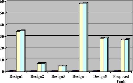
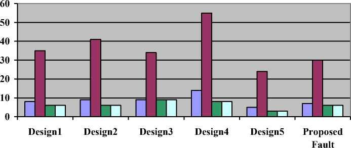
performs highest number of arithmetic and logical operations yet suffers from high quantum cost and absence of fault tolerance property. Design 3 performs very few arithmetic and logical operations yet quantum cost is comparatively high. The proposed ALU holds the minimum quantum cost which support 12 operations and consequently it reduces power consumption, complexity and hardware overhead. Power consumption and other optimization metrics comparison of various ALU designs is given in Table 4 and Table 5 respectively. Proposed fault tolerant ALU based on divide and conquer approach prove to be an efficient design more in terms of power and other optimization metrics like number of operations, number of gates, quantum cost and number of garbage outputs as compare to existing designs as shown in Fig.18 and Fig. 19.
Table 4. Power Consumption Comparison of Various ALU Designs
|
Power consumption(mw) Parameter |
Design1 [6] |
Design2 [7] |
Design3 [7] |
Design 4 [8] |
Design 5[9] |
Proposed Fault tolerant ALU |
|
Logic |
0.19 |
0.02 |
0.01 |
0.16 |
0.06 |
0.04 |
|
Signals |
0.47 |
0.07 |
0.04 |
0.36 |
0.18 |
0.25 |
|
IOS |
34.36 |
6.95 |
4.67 |
57.99 |
28.49 |
27.08 |
|
Total |
35.01 |
7.04 |
4.72 |
58.52 |
28.73 |
27.37 |
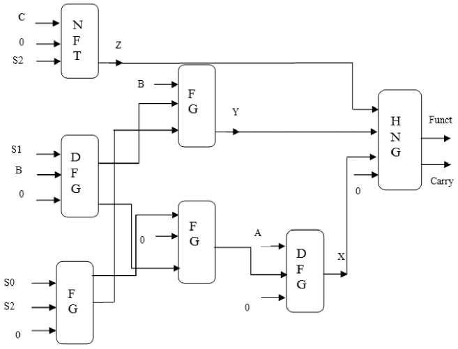
Fig.16. Block diagram of fault tolerant ALU
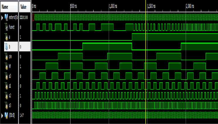
Fig.17. Simulation waveform of fault tolerant ALU
Table 5. Optimization Metrics Comparison of Various ALU Designs
|
ALU DESIGNS/Papers |
Design1 [6] |
Design2 [7] |
Design3 [7] |
Design 4 [8] |
Design 5 [9] |
Proposed Fault tolerant ALU |
|
No. of Gates |
8 |
9 |
9 |
14 |
5 |
7 |
|
Quantum Cost |
35 |
41 |
34 |
55 |
24 |
30 |
|
Arithmetic & Logic operations |
9 |
5 |
4 |
29 |
8 |
12 |
|
N bit ALU(Divide & conquer approach) |
Not possible |
Not possible |
Not possible |
Possible |
Not possible |
Possible |
|
Type of Gates Used |
HNG, MG, Feynman, Fredkin |
Feynman, Fredkin, Toffoli |
Feynman, Fredkin, Peres |
CNOT, Toffoli |
CSA, Toffoli, Fredkin, CNOT |
Fredkin,double Feynman, NFT and HNG |
|
Garbage outputs |
6 |
6 |
9 |
8 |
3 |
6 |
|
Fault tolerance |
No |
No |
No |
No |
No |
Yes |
Tolerant ALU
-
□ Logic □ Signals □ IOS □ Total
Fig.18. Power consumption comparison of various ALU designs
Tolerant ALU
-
□ NO. of Gates □ Quantum Cost □ Garbage Outputs □ No. of operations
Fig.19. Optimization metrics comparison of various ALU designs
-
VI. Conclusions
The proposed ALU Design promises the efficient and the most reliable way to achieve the Fault tolerant reversible design. The RTL code is written using VHDL and simulated using Xilinx ISE design suit 14.2 tool and its performance over existing ALU designs is qualitatively analyzed. Fault tolerance approach using parity preserving gates in combination with other methods will prove to be advantageous for ultra low power robust integrated circuit demanded by many industrial and commercial applications.
References Fault Tolerant ALU using Parity Preserving Reversible Logic Gates
- R.Landauer, "Irreversibility and heat generation in the computing process", IBM Journal of Research and Development, vol.5, no.3, pp.183-191, 1961
- C.Bennett," Logical reversibility of computation",IBM Journal of Research and Development, vol.17, no.6, pp.525-532,1973
- B.Sen, S. Ganeriwal and B.Sikdar,"Reversible logic-based fault-tolerant nanocircuits in QCA", ISRN Electronics, pp.1-9, 2013
- R.Saligram, S.H. Shridhar, A.S. Kulkarni, , H.R, B. and M.K, "Design of parity preserving logic based fault tolerant reversible arithmetic logic unit", International Journal of VLSI Design & Communication Systems, vol. 4, no.3, pp.53-68,2013
- M.Islam and Z.Begum,"Reversible logic synthesis of fault tolerant carry skip BCD adder", Journal of Bangladesh Academy of Sciences,vol. 32, no.2., 2009
- M.Morrison, M. Lewandowski,R. Meana,and N.Ranganathan, "Design of a novel reversible ALU using an enhanced carry look- ahead adder",. 11th IEEE International Conference on Nanotechnology. Portland, Oregon, USA, IEEE, pp.1436-1440,2011
- Y.Syamala and A.TIlak," Reversible arithmetic logic unit",Electronics Computer Technology (ICECT), 3rd International Conference, Kanyakumari.IEEE, pp.207-211,2011
- Z.Guan, W. Li, W.Ding, Y. Hang and L.Ni, L,"An arithmetic logic unit design based on reversible logic gates",Communications, Computers and Signal Processing (PacRim), 2011 IEEE Pacific Rim Conference, Victoria, BC: IEEE, pp.925-931,2011
- R.Singh, S. Upadhyay, S. S, J.KB, and H.SA, "Efficient design of arithmetic logic unit using reversible logic gates, International Journal of Advanced Research in Computer Engineering & Technology (IJARCET), vol.3, no. 4, pp.1474-1477,2014
- V.Veravalli, "Fault tolerance for arithmetic and logic unit",IEEE Southeastcon ,Atlanta, GA,IEEE, pp.329-334,2009
- T.Rakshith and R.Saligram," Parity preserving logic based fault tolerant reversible ALU", Information & Communication Technologies (ICT), 2013 IEEE Conference. JeJu Island, IEEE, pp.485-490, 2013
- N.Sharma, R. Sachdeva, U.Saraswat,R.Yadav and G.Kaur, "Power efficient arithmetic logic unit design using reversible logic",International Journal of Computer Applications, vol.128, no.6, pp.36-41,2015
- A.Majumdar, S. Nayyar and J.Sengar,"Fault tolerant ALU system",Computing Sciences (ICCS), 2012 International Conference, Phagwara, IEEE, pp.255-260,2012
- V.Khorasani,B. Vahdat and M.Mortazavi, "Analyzing area penalty of 32-Bit fault tolerant ALU using BCH code, Digital System Design (DSD), 2011 14th Euromicro Conference, Oulu, IEEE, pp.409-413, 2011
- K.Arunachalam, M. Perumalsamy, C. Sundaram, and J.Kumar, " Design and implementation of a reversible logic based 8-Bit arithmetic and logic Unit", International Journal of Computers and Applications.,Vol.36, no.2, pp. 49-55,2014
