FPGA Implementation of Secure Force (64-Bit) Low Complexity Encryption Algorithm
 Low Complexity Encryption Algorithm")
Author: Shujaat Khan, M. Sohail Ibrahim, Mansoor Ebrahim, Haseeb Amjad
Journal: International Journal of Computer Network and Information Security(IJCNIS) @ijcnis
Article in issue: 12 vol.7, 2015.
Free access
Field-Programmable Gate Arrays (FPGAs) have turned out to be a well-liked target for implementing cryptographic block ciphers, a well-designed FPGA solution can combine some of the algorithmic flexibility and cost efficiency of an equivalent software implementation with throughputs that are comparable to custom ASIC designs. The recently proposed Secure Force (SF) shows good results in terms of resource utilization compared to older ciphers. SF appears as a promising choice for power and resource constrained secure systems and is well suited to an FPGA implementation. In this paper we explore the design decisions that lead to area/delay tradeoffs in a full loop-unroll implementation of SF-64 on FPGA. This work provides hardware characteristics of SF along with implementation results that are optimal in terms of throughput, latency, power utilization and area efficiency.
SF (Secure Force), FPGA, ASIC, WSN (Wireless Sensor Networks), security algorithms, Hardware implementation
Short address: https://sciup.org/15011483
IDR: 15011483
Text of the scientific article FPGA Implementation of Secure Force (64-Bit) Low Complexity Encryption Algorithm
Published Online November 2015 in MECS
Reconfigurable hardware devices are highly captivating platforms for the implementation of encryption algorithms. FPGA implementation of such algorithms is a field of interest for researchers. For the last fifteen years, various implementations with different design tradeoffs have been proposed [2], [3], [4], [5], [6]. Each implementation has its own parametric definition for efficiency of which area, computation cost, power dissipation etc. are a few to name. Data security algorithms can be implemented on FPGA platform in different architectures, such as Iterative Looping, Iterative Looping with Partial Loop Unrolling, Full Loop Unrolling, Pipelining, and Sub-Pipelining [2]. The Secure Force shows good results on image and data encryption on general hardware platform [8]. This paper presents a full loop-unroll architecture of SF (64-bit) implementation on FPGA platform, which provides high throughput at the expense of very low hardware resource utilization. Loop unrolling, also known as loop unwinding, is a loop transformation practice that attempts to optimize the design execution speed at the expense of resource utilization (space-time tradeoff).
In this paper, we have proposed a 64-bit implementation of SF on Altera Cyclone II (EP2C35F672C6N) FPGA using 422/354/139 LEs, which resulted in 2.3/2.6/3.43 Gbps throughput consuming 117.18/117.17/117.12mW power. The rest of the paper is organized as; the literature review is presented in sectio 2, in section 3 we define the working of SF algorithm and its architecture. In section 4 the performance evaluation criteria is discussed. The test results based on these evaluation criteria are presented in section 5. Finally, the paper concludes in the section 6.
-
II. Related Work
This section discusses the detailed research by many scholars in the field of data encryption in WSN. Bahram Rashidi[24] presented an FPGA implementation of an optimized combinational logic based Rijndael S-BOX in AES algorithm. Their attempt is to implement the complex mathematical equations using optimized and combinational logic circuits in order to minimize the dynamic power on FPGA. Their S-BOX implementation acheived a maximum clock frequency of 209.61MHz at the expense of 29mW dynamic power, with the S-BOX logic area of 45 slices. Bahram Rashidi[25] attempt another FPGA implementation of a low power 128-bit Advanced Encryption Standard (AES) algorithm based on a novel asynchronous self-timed architecture for encryption of audio signals. The self-timed architectures are based on asynchronous circuits that perform their function based on hand shake signals. These circuits perform their function independently from other modules which makes these circuits independent of a clock pulse. This work of Bahram Rashidi[25] resulted in a complete AES algorithm implementation on FPGA with 100MHz maximum clock frequency and 283mW power consumption with the logic resource utilization of 2856 slices on a Xilinx Vertix IV FPGA. Joseph Zambreno[6] attempt a hardware implementation of AES on FPGA where they explored the design decisions that lead to area/delay tradeoffs in a single core implementaion. Hoang Trang[11] proposed an efficient FPGA implementation of the AES algorithm. They used iterative looping approach with the block and key size of 128-bits look-up table implementation of AES S-BOX. Tim Good[13] proposed two implementaions of AES algorithm on FPGA that are claimed to be the smallest and the fastest implementations of AES on FPGA. The proposed fastest implementaion acheived a throughput of 25Gbps while the smallest only requires as low as 2 block memories and 124 slices to achieve 2.2Mbps throughput. Jingli Zheng[26] proposed a light weight symmetric key algorithm based on feistal structure. Their algorithm architecture is similar to our proposed algorithm in many ways such as; it has less number of encryption rounds and the scrambling of data is done in a simplified way, which makes their algorithm computationally inexpensive as compared to other benchmark algorithms. Thus, low complexity algorithms perform better when low battery power, efficient resource utilization, and adequate security is required. Hassen Mestiri[27] attempt efficient FPGA hardware implementation of Secure Hash Function SHA-2. They optimized SHA-256 and SHA-512, and implemented their proposed design on Xilinx Vertix-5 FPGA with logic area as low as 387 slices for SHA-256 which resulted in a throughput of 1.58Gbps with the maximum operating frequency of 202.54 MHz. For SHA-512, the area is 874 slices with 2.20 Gbps throughput and 176.06 MHz maximum operating frequency.
It is evident from the summary of our literature review that low complexity and light weight symmetric key algorithms are suitable for hardware imlementations as they require less area and their performance is comparable with standard encryption algorithms such as DES and AES in terms of throughput, power and operating frequency.
-
III. The Secure Force Algorithm
Due to the advancement in the communication technology, various applications come up with numerous challenges including power, security, scalability, and design simulation problems [17], [18], [19]. Power constrained networks like Wireless Sensor Networks (WSN) demand an algorithm which can provide a reliable security with low power utilization. Recently proposed
Secure Force algorithm is one of the candidates for WSN. The design of SF algorithm provides low-complexity architecture for implementation in WSN. To ensure energy efficient implementation, it is suggested to lower the number of encryption rounds [23]. In SF each encryption round encompass six simple arithmetic operations on 4-bit data to ensure security. This creates the adequate confusion and diffusion of data to confront various types of attacks. The key expansion process, implemented at the decoder, involves complex mathematical operations such as multiplication, permutation, rotation and transportation to generate keys for the encryption process. This shifted the computational burden to the decoder and indirectly, this will help to increase the lifespan of the sensor nodes. However, the generated keys must be transmitted securely to the encoder for the encryption process. The LEAP (Localized Encryption and Authentication Protocol) is employed for this case which is energy efficient, robust and secure key management protocol designed for WSN. Overall, the process of SF algorithm consists of 4 major blocks. The detail description of search block of the proposed algorithm can be found in [1].
Key Expansion Block: Key expansion is the primary process that is used to generate different keys for encryption and decryption. Different operations are performed in order to create confusion and diffusion. This is to reduce the possibility of weak key as well as to increase the key strength. The round keys (Kr) are derived from the input cipher key by means of the key schedule. The process consists of two components: key expansion and round key selection. The key expansion performs logical operations (XOR, XNOR), left shifting (LS), matrix multiplication using fix matrix (FM), permutation using P-table and transposition using T-table. The block diagram of key expansion block is shown in fig. 1.
Key Management Protocol: The key can be securely sent to the encoder with the aid of LEAP [7]. It is a simple and energy efficient protocol designed for large scale WSN, which allows secure key establishment through the use of four types of keys. They are known as the individual key, group key, cluster key, and pair wise shared key.
Encryption Block: The encryption process is initiated once the keys generated by the key expansion block are securely received by the encoder through the secure communication channel created by using the LEAP protocol. In the encryption process, simple operations, which include AND, OR, XOR, XNOR, left shift (LS), substitution (S boxes) and swapping operations, are performed to create confusion and diffusion. The detailed block diagram of the encryption block is shown in fig. 2.
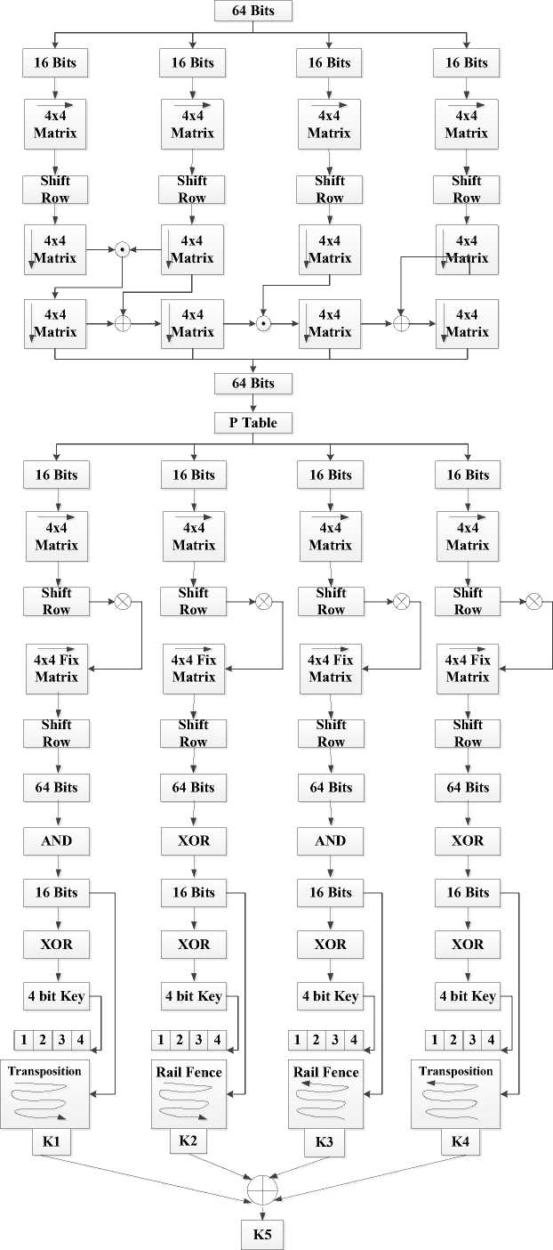
Fig. 1. Block Diagram of Key Expansion Block
64 Bits
V 1 *
32 Bits 32 Bits
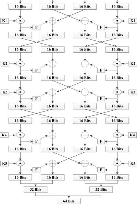
Fig. 2. Block Diagram of Encryption Process
Decryption Block: The decryption process is just the reverse of the encryption process described above.
-
IV. Proposed Secure Force Architecture For Fpga Implementation
Implementation of a cryptographic algorithm on hardware holds many choices of implementation techniques including pipelining, loop unrolling (full, partial, and e.t.c.), datapath width optimization, and substitution box designs. However, the full parallel loop unroll architecture is preferred where high throughput is required [13].
The proposed full loop-unroll FPGA architecture for SF consists of three modules; key generation module, encryption module, and decryption module. The top level entity named SF combines all three modules together to form a complete single-unit to implement it on Altera DE2 board. First, a 64-bit key passes through the key generator which generates K1, K2, K3, K4, and K5 that are also 64-bit keys for all five rounds as mentioned in [1]. These five keys (K1 to K5) will be used by the encryption block which takes the plain text from the IOs and converts it into a cipher text of 64-bits by applying the encryption process, which consists of five rounds. In each round different keys from K1 to K5 will be used. In the final step, the encrypted message with the same key used for encryption is passed to the decryption block which applies the reverse encryption process which also consists of five rounds, and uses the same keys (K1 to K5) to decrypt the encrypted message back to a plain text.
In order to investigate the performance of individual block each encryption, decryption and key expansion block is implemented separately. The detailed description of sub-modules of SF will be given in their respective sections.
Key Expansion Block
Key expansion is the primary process that is used to generate keys for encryption and decryption process. Different operations are performed in order to create confusion and diffusion. This is to reduce the possibility of weak keys as well as to increase the key strength. The round keys (Kr) are derived from the input cipher key by means of the key schedule. The process consists of two components: key expansion and round key selection. The key expansion performs logical operations (XOR, XNOR), left shifting (LS), matrix multiplication using fix matrix (FM), permutation using P-table and transposition using T-table. The detailed block diagram of key expansion and round scheduling is available in [1].
The proposed architecture divides the key expansion sub-blocks into two categories
Bit Position Interchange Module
Shifting Module, Transpose, and P-Table are the modules that utilize no logic elements as these modules involve the interchange of the bits position only.
Functional Logic Block
Logical operations (XOR, XNOR, AND, OR), Fixed matrix multiplication, Transposition, and Adder block are the functional logic blocks of SF key expansion process. In these blocks, arithmetic and logic operations are performed. The logical operation block performs simple logic functions whereas the fixed matrix multiplication, transposition and adder block are custom designed to simplify the complex arithmetic operations to reduce the resource utilization and computational delay.
Fixed Matrix Multiplication: As proposed in [1], the key expansion block requires the multiplication of four fixed matrices. The fixed matrix multiplication produces bounded results. We exploited this and applied the distributed arithmetic technique [9], which converts this complex multiplication task into simple pattern look-up problem. Fig. 3, shows the fixed multiplication block, there are four of such multiplication blocks in the design. Since the multiplication produces bounded results every time, so, using distributed arithmetic techniques, the result of each multiplication bit is achieved by matching the multiplication result pattern on a look-up table.
Adder Block: The adder block is the sub-block of the fixed matrix multiplication process. We designed a lookup table for all possible outcomes of the fixed matrix multiplication and repeatedly used this block with different input bits configurations. The implementation of adder block is shown in Fig. 4.
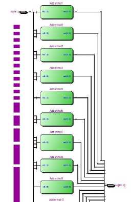
Fig. 3. Fixed Matrix Multiplication Block
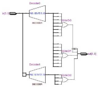
Fig. 4. Adder Block
Transposition Block: This block also interchanges the bits position, but this interchange process is the function of 4-bit inputs generated from the XOR block (logical operations). This conditional interchanging takes place with the help of multiple multiplexors as shown in Fig. 5.
include simple logical operators, shifting block, ED-block/F-block (encryption-decryption or functional block), and substitution (S-boxes). The circuit diagram of encryption and decryption blocks are shown in Fig. 6 and Fig. 7 respectively.
The proposed architecture for SF Encryption and Decryption contains the following categories of modules.
Bit Position Interchange Module
Shifting blocks are the bit position interchanging modules used in the ED function. In these blocks only the interchange of bits take place, and no logical operations are performed, hence this module occupy no hardware resources.
Functional Logic Block
Logical operations (XOR, XNOR, AND, OR), ED function (F-function), and SBOX are the functional logic blocks of SF Encryption/Decryption process. In these blocks, complex logic operations are performed. The logical operation block performs simple logic functions such as XOR, XNOR, AND whereas the complex logical operation of F-function is custom designed as ED (Encryption/Decryption) block, and to simplify the design implementation, substitution(S-boxes) are designed separately.
F-Function (ED function): It is the major element of encryption algorithm that induces diffusion of data. It performs substitution, AND, OR and left shifting (LS) operations on 16 bits of data as shown in Fig. 8.
Substitution Box (S-BOX): F function uses four different types of SBOXs, constructed by using different operations to mix the data and to make the result more complex. SBOX results are generated in such a way that the middle part of each 4 bits data is considered as the column selector and the corner bits are considered as the row selector. Hardware implementation of SBOXs is shown in Fig. 9 to Fig. 12.
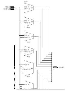
Fig. 5. Transposition Block
Encryption/Decryption Block
Encryption and decryption can be done with the same operations using different approaches. These blocks
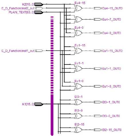
Fig. 6. Top level view of encryption block
E D Function:in5t1
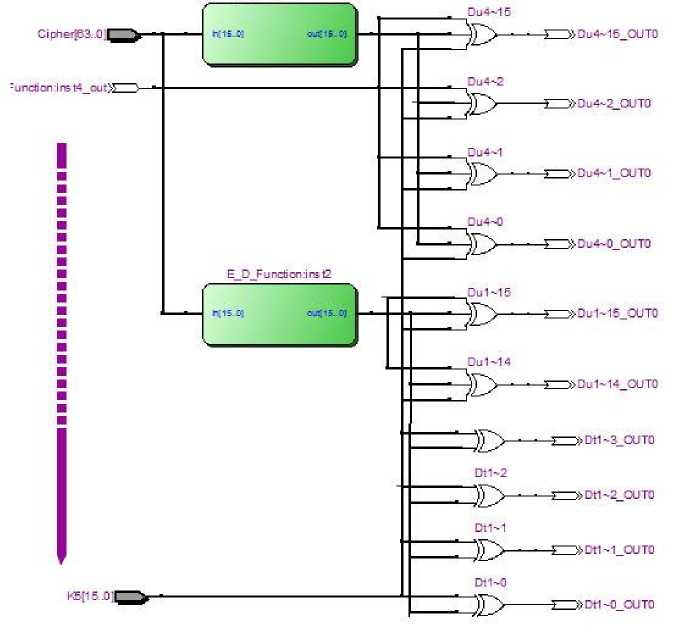
Fig. 7. Top level view of decryption block with ED-Function
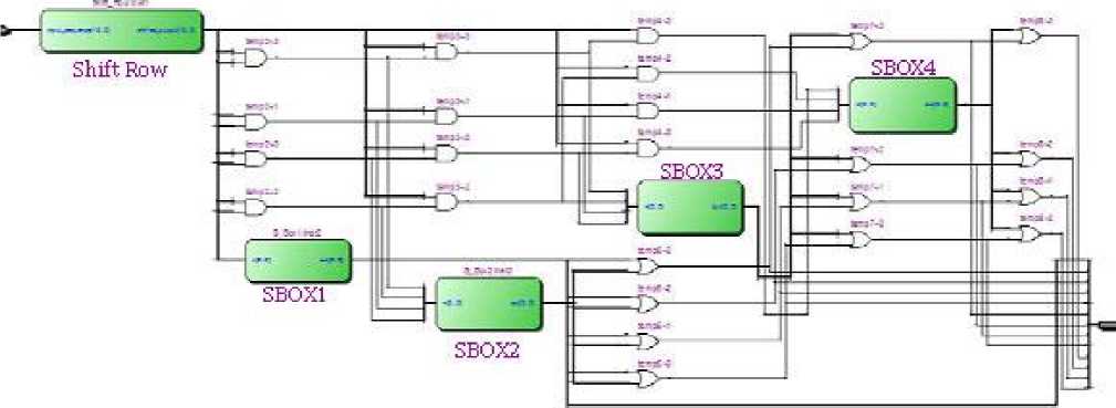
Fig. 8. ED-Function internal view
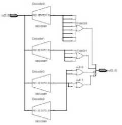
Fig. 9. SBOX1
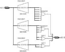
Fig. 10. SBOX2
Fig. 11. SBOX3
Fig. 12. SBOX4
-
V. Performance Evaluation Criteria
Evaluation of SF algorithm on FPGA was carried out on certain well know parameters used by various authors [10], [11], [12], [13], [14], [15] for the assessment of the performance of their proposed FPGA based designs. A brief description of the design evaluation parameters of SF implementation are mentioned below.
Propagation Delay
Propagation Delay is defined as the length of time which exists between the edges of a signal propagating from an input of a circuit to the output. Since the proposed design is based on a full loop-unroll architecture, so propagation delay is suggested as the amount of time required for the slowest signal to propagate from the input of the circuit to the output.
Maximum Operating Frequency
The maximum operating frequency defines the maximum clock rate at which the circuit can process the data without generating errors. It can be calculated as
MOF =
1 MPD
Where MOF is maximum operating frequency and MPD is maximum propagation delay.
Throughput
The amount of data that can be encrypted/decrypted in one second defines the throughput of hardware based encryption circuit. The throughput is measured in bits per second and can be calculated by the given relation:
Throughput = frequency x wordsize (2)
Area
The area utilization of an FPGA based design is proportional to the number of IOs and the number of Logic Elements (LE) used. An LE contains [16].
-
• A four-input look-up table (LUT)
-
• A programmable register and carry chain connection.
-
• A register chain connection.
-
• The ability to drive all types of interconnects
-
• Support for register packing and feedback.
Power Consumption
The power consumption in FPGAs is divided into three components
-
1) Static Power
This is the power consumed by the FPGA when no signals are toggling. This can be the pre-program static power and it can also be the power being consumed by the device when there is no clock signal provided.
-
2) Dynamic Power
This is the additional power consumed by the circuit related signals which include the charging and discharging of capacitive loads and the toggling of signals. Higher clock frequencies result in higher dynamic power.
-
3) I/O Power
The I/O power is the power consumed by the I/O blocks.
-
VI. Experimental Results
-
A. Propagation Delay
Propagation delay reports longest delay in nanoseconds between the edges of a signal propagating from an input port to an output port.
-
• RR shows the longest delay measured from rising edge to rising edge.
-
• FF shows the longest delay measured from falling edge to falling edge.
Note that, in propagation delay, the highest delay (worst-case) is important. The propagation delay results for encryption, decryption and key expansion block are shown in table 1, table 2 and table 3. The timing/propagation delay results are mentioned in nanoseconds.
Table 1. Propagation Delay for Encryption
|
PARAMETER |
RR (ns) |
FF (ns) |
|
MEAN TIME |
19.83971 |
19.8397111 |
|
MAX TIME |
27.847 |
27.847 |
|
STD TIME |
6.349543 |
6.34954339 |
Table 2. Propagation Delay for Decryption
|
PARAMETER |
RR (ns) |
FF (ns) |
|
MEAN TIME |
18.4047 |
18.4046963 |
|
MAX TIME |
24.638 |
24.638 |
|
STD TIME |
5.647841 |
5.64784058 |
Table 3. Propagation Delay for Key Expansion
|
PARAMETER |
RR (ns) |
FF (ns) |
|
MEAN TIME |
13.04696 |
13.0469631 |
|
MAX TIME |
18.681 |
18.681 |
|
STD TIME |
2.844862 |
2.84486153 |
The results depicted in table 1 and table 2 show a slightly high propagation delay, and it is due to the fact that the proposed implementation is based on full-loop-unroll architecture which elongates the electrical paths in the circuit (since each loop iteration is unrolled and is transformed into a separate circuit). Another reason for the higher propagation delay is that the experimental setup was carried out on an educational purpose FPGA board (Altera DE2), which is incomparable to the professional development boards used in [6], [13], [14], [20].
Table 4 shows the comparison of SF with some popular implementations of Advance Encryption Standard (AES) on FPGA platforms. It shows that the proposed implementation can attain a maximum operating frequency of 35.9/40.6 MHz with 2.3/2.6 Gbps throughput for encryption/decryption where as key expansion process can be executed at 53.5 MHz(max) to provide 3.43 Gbps throughput.
Table 4. Maximum Operating Frequency and Throughput
|
Design |
Max. Operating Frequency (MHz) |
Throughput (Mbps) |
|
[20] |
140.390 |
352 |
|
[14] |
350 |
4100 |
|
[11] |
287 |
647 |
|
[13] |
196.1 |
25107 |
|
[6] |
184.16 |
23570 |
|
SF(64) |
35.9/40.6/53.5 |
2300/2600/3430 |
SF performs reasonably well in throughput and maximum operating frequency. The table shows the comparison of SF with some recent research work on the implementation of cryptographic algorithm on reconfigurable hardware/FPGA. Despite the fact that the propagation delay of proposed SF design is slightly high which is due to incompetent hardware used, SF shows very promising results in terms of throughput and maximum operating frequency.
Area
Area is the measure of Logic Element utilization of a circuit. The table 5 shows that SF can be implemented on Altera Cyclone II FPGA with as low as 354 Logic Elements (LE). Area/resource utilization is also calculated in terms of the number of slices (LCs in terms of Xilinx FPGA). The slice (LC) to logic element (LE) ratio is 1.125:1 as provided in [21].
Table 5. Logic Resource (Area) Utilization
|
Design |
Device |
(Slices) Enc/Dec |
% Area |
|
[20] |
XCV600BG560-6 |
1853 |
26 |
|
[14] |
Vertix-5 |
800/1100 |
- |
|
[11] |
XC3S200 |
148 |
3.43 |
|
[13] |
XC3S2000-5 |
17425 |
37.82 |
|
[6] |
XC2V4000 |
16938 |
73.52 |
|
SF(64) |
EP2C35F672C6N |
476/400/160 |
1.27/1.07/0.42 |
The resource utilization results indicate that SF (64-bit) is a very light-weight algorithm in terms of area/resource utilization. Table 5 shows that SF uses 1.27/1.07 percent of the FPGA’s hardware resources which is among the most area efficient implementations listed in the table 5. As listed in the table [11] has the lowest resource utilization but it is evident from table 4 that there is a lack of performance in terms of throughput, while SF, in contrast shows high throughput at the cost of very low logic resource utilization. The Throughput/Area ratio of above mentioned implementations are as follows 0.19[20], 5.125/3.723 [14], 4.37[11], 1.44[13], 1.39[6], and
4.83/6.5/21.44 for SF (64) proposed. According to the literature review depicted in the table 4 and table 5, it is evident that on FPGA perform SF can perform better than many other standard AES implementations, in terms of throughput/area ratio. As far as we know this implementation of SF is the first FPGA implementation with such throughput/area ratio.
Power Consumption
Power consumption of a circuit is divided in Static, Dynamic and IO Power consumption as mentioned in section 4. The table 6 presents the total power, static power and IO power consumption.
Table 6. Power Dissipation for Encryption/Decryption/Key-Expansion in mili-Watts
|
Total Thermal Power Dissipation |
117.18/117.17/117.12 |
|
Core Static Thermal Power Dissipation |
79.95/79.95/79.95 |
|
I/O Thermal Power Dissipation |
37.23/37.22/37.17 |
In our literature review, we observed that many researchers have mentioned the dynamic power of their design. Dynamic power is the power dissipation caused by the clock (or switching of transistors). The proposed FPGA implementation of SF is based on full-loop unroll architecture which has no clock (switching activity) hence it has zero dynamic power, but for comparison purpose we have calculated the dynamic power of our design mathematically as [22]:
P = C X a X f X V2 (3)
Where is assumed as the capacitive load of the IO, (50% activity on every clock) is the average switching activity, is the operating frequency, and is the IO voltage which yields 141.45mW of total dynamic power.
-
VII. Conclusion
In this paper we implemented the SF (64-bit) on FPGA platform using Full Loop Unrolling technique. The proposed FPGA design performs reasonably well in terms of power consumption and resource utilization. The FPGA implementation of SF provides throughput of 2.3/2.6/3.43 Gbps by using only 476/400/160 slices and 117.18/117.17/117.12mW power, which is comparable with various implementations of AES. The proposed implementation is the first FPGA implementation of Secure Force (SF-64) algorithm. Complete Verilog code for altera DE2 board FPGA and MATLAB code for software implementation is freely available online at authors research gate link:
-
[1] Ebrahim, Mansoor, and Chai Wai Chong. "Secure Force: A low-complexity cryptographic algorithm for Wireless Sensor Network (WSN)." Control System, Computing and Engineering (ICCSCE), 2013 IEEE International Conference on. IEEE, 2013.
-
[2] Elbirt, Adam J., et al. "An FPGA-based performance evaluation of the AES block cipher candidate algorithm finalists." Very Large Scale Integration (VLSI) Systems, IEEE Transactions on 9.4 (2001): 545-557.
-
[3] Standaert, Francois-Xavier, et al. "Efficient implementation of Rijndael encryption in reconfigurable hardware: improvements and design tradeoffs."
Cryptographic Hardware and Embedded Systems-CHES 2003. Springer Berlin Heidelberg, 2003. 334-350.
-
[4] Ji, Bing, Liejun Wang, and Qinghua Yang. "New Version of AES-ECC Encryption System Based on FPGA in WSNs." Journal of Software Engineering 9.1 (2015): 8795.
-
[5] Chodowiec, Paweł, and Kris Gaj. "Very compact FPGA implementation of the AES algorithm." Cryptographic Hardware and Embedded Systems-CHES 2003. Springer Berlin Heidelberg, 2003. 319-333.
-
[6] Zambreno, Joseph, David Nguyen, and Alok Choudhary. "Exploring area/delay tradeoffs in an AES FPGA implementation." Field Programmable Logic and Application. Springer Berlin Heidelberg, 2004. 575-585.
-
[7] E. Biham and A. Shamir, “Differential cryptanalysis of data encryption standard”. Berlin, Germany: SpringerVerlag, 1993.
-
[8] Khan, Shujaat, Mansoor Ebrahim, and Kafeel Ahmed Khan. "Performance Evaluation of Secure Force Symmetric Key Algorithm." (2015).
-
[9] Llamocca, Daniel, Marios Pattichis, and G. Alonzo Vera. "Partial reconfigurable FIR filtering system using distributed arithmetic." International Journal of Reconfigurable Computing 2010 (2010): 4.
-
[10] Gaj, Kris, Ekawat Homsirikamol, and Marcin Rogawski. "Fair and comprehensive methodology for comparing hardware performance of fourteen round two SHA-3 candidates using FPGAs." Cryptographic Hardware and Embedded Systems, CHES 2010 . Springer Berlin Heidelberg, 2010. 264-278.
-
[11] Huang, Chi-Wu, et al. "Compact FPGA implementation of 32-bits AES algorithm using Block RAM." TENCON 2007-2007 IEEE Region 10 Conference . IEEE, 2007.
-
[12] Chang, Chi-Jeng, et al. "High throughput 32-bit AES implementation in FPGA." Circuits and Systems, 2008. APCCAS 2008. IEEE Asia Pacific Conference on . IEEE, 2008.
-
[13] Good, Tim, and Mohammed Benaissa. "AES on FPGA from the fastest to the smallest." Cryptographic Hardware and Embedded Systems–CHES 2005 . Springer Berlin Heidelberg, 2005. 427-440.
-
[14] Bulens, Philippe, et al. "Implementation of the AES-128 on Virtex-5 FPGAs." Progress in Cryptology– AFRICACRYPT 2008 . Springer Berlin Heidelberg, 2008. 16-26.
-
[15] Kong, Jia Hao, Li-Minn Ang, and Kah Phooi Seng. "A comprehensive survey of modern symmetric
cryptographic solutions for resource constrained environments." Journal of Network and Computer
Applications 49 (2015): 15-50.
-
[16] Altera ® Cyclone II Architecture. Website: http://www.altera.com/literature/hb/cyc2/cyc2_cii51002.p df.
-
[17] M. Ebrahim, S. Khan and U.B. Khalid,” Symmetric algorithm survey: a comparative analysis”. International Journal of Computer Applications 61(20), January 2013, pp. 12-19. USA
-
[18] Ebrahim, Mansoor, Shujaat Khan, and Syed Sheraz Ul Hasan Mohani. "Peer-to-Peer Network Simulators: an Analytical Review." Asian Journal of Engineering Science and Technology (2012).
-
[19] Ebrahim, Mansoor, Shujaat Khan, and UmerBin Khalid. "Security Risk Analysis in Peer 2 Peer System; An Approach towards Surmounting Security Challenges." Asian Journal of Engineering Science and Technology (2012).
-
[20] Borkar, Atul M., R. V. Kshirsagar, and M. V. Vyawahare. "FPGA implementation of AES algorithm." Electronics Computer Technology (ICECT), 2011 3rd International Conference on . Vol. 3. IEEE, 2011.
-
[21] Šćekić, Ognjen. "FPGA Comparative Analysis."
-
[22] Dynamic Power Reduction in Flash FPGAs. AC323, Microsemi.
-
[23] R. Chandramouli, S. Bapatla, and K. P. Subbalakshmi, “Battery power-aware encryption”, ACM Transactions on Information and System Security, Vol. 9, No. 2, May 2006, pp. 162–18.
-
[24] Rashidi, Bahram, and Bahman Rashidi. "Implementation of an optimized and pipelined combinational logic rijndael S-Box on FPGA." International Journal of Computer Network and Information Security (IJCNIS) 5.1 (2013): 41.
-
[25] Rashidi, Bahram, and Bahman Rashidi. "FPGA Based A New Low Power and Self-Timed AES 128-bit Encryption Algorithm for Encryption Audio Signal." International Journal of Computer Network and Information Security (IJCNIS) 5.2 (2013): 10.
-
[26] Zheng, Jingli, Zhengbing Hu, and Chuiwei Lu. "A Lightweight Symmetric Encryption Algorithm Based on Feistel Cryptosystem Structure." International Journal of Computer Network and Information Security (IJCNIS) 7.1 (2014): 16.
-
[27] Mestiri, Hassen, et al. "Efficient FPGA Hardware Implementation of Secure Hash Function SHA-2." International Journal of Computer Network and Information Security (IJCNIS) 7.1 (2014): 9.
References FPGA Implementation of Secure Force (64-Bit) Low Complexity Encryption Algorithm
- Ebrahim, Mansoor, and Chai Wai Chong. "Secure Force: A low-complexity cryptographic algorithm for Wireless Sensor Network (WSN)." Control System, Computing and Engineering (ICCSCE), 2013 IEEE International Conference on. IEEE, 2013.
- Elbirt, Adam J., et al. "An FPGA-based performance evaluation of the AES block cipher candidate algorithm finalists." Very Large Scale Integration (VLSI) Systems, IEEE Transactions on 9.4 (2001): 545-557.
- Standaert, Francois-Xavier, et al. "Efficient implementation of Rijndael encryption in reconfigurable hardware: improvements and design tradeoffs." Cryptographic Hardware and Embedded Systems-CHES 2003. Springer Berlin Heidelberg, 2003. 334-350.
- Ji, Bing, Liejun Wang, and Qinghua Yang. "New Version of AES-ECC Encryption System Based on FPGA in WSNs." Journal of Software Engineering 9.1 (2015): 87-95.
- Chodowiec, Paweł, and Kris Gaj. "Very compact FPGA implementation of the AES algorithm." Cryptographic Hardware and Embedded Systems-CHES 2003. Springer Berlin Heidelberg, 2003. 319-333.
- Zambreno, Joseph, David Nguyen, and Alok Choudhary. "Exploring area/delay tradeoffs in an AES FPGA implementation." Field Programmable Logic and Application. Springer Berlin Heidelberg, 2004. 575-585.
- E. Biham and A. Shamir, "Differential cryptanalysis of data encryption standard". Berlin, Germany: Springer-Verlag, 1993.
- Khan, Shujaat, Mansoor Ebrahim, and Kafeel Ahmed Khan. "Performance Evaluation of Secure Force Symmetric Key Algorithm." (2015).
- Llamocca, Daniel, Marios Pattichis, and G. Alonzo Vera. "Partial reconfigurable FIR filtering system using distributed arithmetic." International Journal of Reconfigurable Computing 2010 (2010): 4.
- Gaj, Kris, Ekawat Homsirikamol, and Marcin Rogawski. "Fair and comprehensive methodology for comparing hardware performance of fourteen round two SHA-3 candidates using FPGAs." Cryptographic Hardware and Embedded Systems, CHES 2010. Springer Berlin Heidelberg, 2010. 264-278.
- Huang, Chi-Wu, et al. "Compact FPGA implementation of 32-bits AES algorithm using Block RAM." TENCON 2007-2007 IEEE Region 10 Conference. IEEE, 2007.
- Chang, Chi-Jeng, et al. "High throughput 32-bit AES implementation in FPGA." Circuits and Systems, 2008. APCCAS 2008. IEEE Asia Pacific Conference on. IEEE, 2008.
- Good, Tim, and Mohammed Benaissa. "AES on FPGA from the fastest to the smallest." Cryptographic Hardware and Embedded Systems–CHES 2005. Springer Berlin Heidelberg, 2005. 427-440.
- Bulens, Philippe, et al. "Implementation of the AES-128 on Virtex-5 FPGAs." Progress in Cryptology–AFRICACRYPT 2008. Springer Berlin Heidelberg, 2008. 16-26.
- Kong, Jia Hao, Li-Minn Ang, and Kah Phooi Seng. "A comprehensive survey of modern symmetric cryptographic solutions for resource constrained environments." Journal of Network and Computer Applications 49 (2015): 15-50.
- Altera ® Cyclone II Architecture. Website: http://www.altera.com/literature/hb/cyc2/cyc2_cii51002.pdf.
- M. Ebrahim, S. Khan and U.B. Khalid," Symmetric algorithm survey: a comparative analysis". International Journal of Computer Applications 61(20), January 2013, pp. 12-19. USA
- Ebrahim, Mansoor, Shujaat Khan, and Syed Sheraz Ul Hasan Mohani. "Peer-to-Peer Network Simulators: an Analytical Review." Asian Journal of Engineering Science and Technology (2012).
- Ebrahim, Mansoor, Shujaat Khan, and UmerBin Khalid. "Security Risk Analysis in Peer 2 Peer System; An Approach towards Surmounting Security Challenges." Asian Journal of Engineering Science and Technology (2012).
- Borkar, Atul M., R. V. Kshirsagar, and M. V. Vyawahare. "FPGA implementation of AES algorithm." Electronics Computer Technology (ICECT), 2011 3rd International Conference on. Vol. 3. IEEE, 2011.
- Šćekić, Ognjen., Ognjen. "FPGA Comparative Analysis."
- Dynamic Power Reduction in Flash FPGAs. AC323, Microsemi.
- R. Chandramouli, S. Bapatla, and K. P. Subbalakshmi, "Battery power-aware encryption", ACM Transactions on Information and System Security, Vol. 9, No. 2, May 2006, pp. 162–
- Rashidi, Bahram, and Bahman Rashidi. "Implementation of an optimized and pipelined combinational logic rijndael S-Box on FPGA." International Journal of Computer Network and Information Security (IJCNIS) 5.1 (2013): 41.
- Rashidi, Bahram, and Bahman Rashidi. "FPGA Based A New Low Power and Self-Timed AES 128-bit Encryption Algorithm for Encryption Audio Signal."International Journal of Computer Network and Information Security (IJCNIS)5.2 (2013): 10.
- Zheng, Jingli, Zhengbing Hu, and Chuiwei Lu. "A Light-weight Symmetric Encryption Algorithm Based on Feistel Cryptosystem Structure." International Journal of Computer Network and Information Security (IJCNIS) 7.1 (2014): 16.
- Mestiri, Hassen, et al. "Efficient FPGA Hardware Implementation of Secure Hash Function SHA-2." International Journal of Computer Network and Information Security (IJCNIS) 7.1 (2014): 9.
