
Frictional scanning probe lithography of advanced materials for dielectric nanophotonics
Journal: Computer Optics @computer-optics
Section: Дифракционная оптика, оптические технологии
Article in issue: 2 т.50, 2026.
Free access
Creating photonic circuits based on advanced dielectric nanophotonic materials is complicated by the difficulty of selecting effective etchants when using standard lithography methods. We propose a universal approach of frictional mechanical scanning probe lithography, which consists of the local removal of material using a sharp diamond probe tip. We demonstrate planar waveguides and disk microresonators made from 200 nm thick GaP layer grown on sapphire substrate and a 40 nm thick MoSe2microdisk cavities exhibiting an optical quality factor reaching 100.
Similar articles in the section Electrical engineering
Short address: https://sciup.org/140314861
IDS: 140314861 | DOI: 10.18287/COJ1838
Text of the scientific article Frictional scanning probe lithography of advanced materials for dielectric nanophotonics
The miniaturization of photonic devices necessitates the utilization of materials that facilitate light localization. There are several approaches that provide localization. Among these, plasmonics [1] and dielectric nanophotonics [2] can be distinguished. A notable disadvantage of plasmonics is the relatively substantial losses associated with it, which result in significant light attenuation within plasmonic waveguides. Objects of dielectric nanophotonics, which are typically wide-bandgap semiconductors or dielectrics, are not subject to this disadvantage. However, the localization of light in these materials is contingent upon the fulfillment of a specific condition. Specifically, the dimensions of the object must satisfy the inequality x < X/2 n, where x represents the object's sizes, X denotes the wavelength of light, and n indicates the refractive index. Consequently, to ensure effective localization, it is imperative to utilize materials with the highest attainable refractive index.
Among the well-known classical semiconductor materials, Si [3] and GaP [4] can be distinguished with a refractive index reaching 3.5. However, Si is not transparent in the visible range. It is noteworthy that classical lithography methods (photolithography, electron lithography) have been demonstrated to be effective for Si and GaP, and photonic circuit units have been demonstrated [5, 6]. In recent years, there has been an active search for materials with a high refractive index, with parameters that exceed those of Si and GaP. Among these materials, van der Waals (vdW) materials, hexagonal boron nitride (hBN), transition metal dichalcogenides (TMD) with a refractive index reaching 5, and halide perovskites are particularly noteworthy [7, 8]. It is important to note that the rate of emergence of promising materials for dielectric nanophotonics is currently increasing [9].
Conversely, the utilization of proven electron beam lithography (EBL) and photo lithography approaches remain elusive for these materials, primarily due to the necessity of identifying effective etchants. Additionally, emerged mask resist removers can etch the material besides the resist. However, a sufficient progress of the EBL implementation for the TMD [10 – 13] and hBN [14] was recently demonstrated [15]. Besides the abovementioned methods a maskless focused ion beam milling can be used. Unfortunately, this approach induces defects in the TMD [16].
Consequently, the development of a universal lithography method that facilitates the fabrication of prototypes of photonic circuit units is crucial. Recently, a frictional mechanical scanning probe lithography (f-SPL) method was developed. The utilization of the f-SPL method has yielded several notable outcomes, including the fabrication of planar resonator gratings from quasi-two-dimensional halide perovskites [17] and the facilitation of exciton-polaritons at ambient temperatures. The creation of microdisk resonators with a diameter of approximately 2 micrometers from WS 2 [18] and GaAs [19] has been achieved, exhibiting an optical quality factor reaching 700 in the visible range [18].
The aim of this study was to examine the potential of scanning probe lithography for the fabrication of photonic circuit nodes from promising dielectric nanophotonics materials.
Samples and methods
In order to create an optical cavity that localizes light, it is necessary to take into account not only the use of high refractive index materials, but also the refractive index of the environment. Therefore, it is essential that the refractive index of the substrate supporting the cavity be as low as possible. To realize this configuration, two different systems were proposed for the study. The first of these was the GaP layer that was grown on sapphire. The second was a bulk MoSe2 flakes exhibited a range of thicknesses, which were meticulously transferred onto a SiO2 substrate with a thickness of 200 nm. Sapphire exhibits a refractive index of 1.75, while SiO2 has a refractive index of 1.45. The GaP layer, with a thickness of 200 nanometers, was grown on a sapphire substrate by molecular beam epitaxy. A comprehensive overview of the growth process is provided in the reference [6].
The lithographic process was carried out on a Ntegra Aura atomic force microscope (AFM) (NT-MDT), employing DRP_IN (Tipsnano) probes equipped with single-crystal diamond tips with a curvature radius of 10 nm. The process employed the frictional mechanical scanning probe lithography (f-SPL), a method exhibiting a 20 nm lateral resolution of the lithography for the TMD monolayer [20 – 22]. In f-SPL method, material is removed from the surface in the contact area when the tip and the surface come into contact (the tip "scratches" the surface). It should be noted that for bulk structures the lateral resolution decreases with increasing of the carved nanogroove depth, when the depth of the microrelief exceeds the tip's curvature radius. Moreover, due to the complex and uncontrolled faceting of the pyramid, the shape of the nanogroove depends on the both pyramid shape and the probe’s moving direction [19, 23].
In the context of van der Waals material such as MoSe 2 , it has been observed that the degree of hardness within the layer significantly surpasses that of the perpendicular direction relative to the layer's plane. This phenomenon indicates that increasing the pressing force does not result in an increase in the cutting depth; rather, it leads to the peeling off the layers in a substantial area. To address this challenge, the frictional force lithography method was developed. The method is characterized as frictional due to the repetitive application of the lithographic pattern with minimal pressure force ( F ). This modest force enables the precise removal of several atomic or molecular layers with each repetition.
It is noteworthy that despite the high hardness of transition metal dichalcogenides, and the GaP, the diamond tip remained undamaged when the appropriate force was applied to the surface. The f-SPL method was employed to create disk microresonators and strip waveguides (see Fig. 1 a ). The vectoral lithographic pattern for the disk cavity is illustrated in Fig. 1 b . The template consists of concentric circles with a spacing smaller than the width of a single nanogroove created by the tip. This allows for efficient material removal and separation of the microdisk from the layer. The circles are slightly offset in the template due to manual selection of their centers in the AFM software. The utilization of GaP layers in lithography was meticulously chosen to showcase analogous capabilities to conventional lithography techniques in the fabrication of nanophotonic structures by f-SPL.
A micro-photoluminescence (PL) spectrum was measured for the MoSe2 disk cavities to detect the potential presence of whispering gallery modes (WGMs) induced by the disk shape of the cavity. The spectra were measured out at room temperature (300 K) using a Horiba LabRAM HR Evolution UV-VIS-NIR (Horiba Jobin Yvon, France) spectrometer equipped with a confocal microscope. The spectra were measured using the continuous-wave excitation at 532 nm of an Nd:YAG laser (Torus, Laser Quantum, UK) with a power on the samples of approximately 4 mW. The PL spectra were recorded using an 1800 grooves/mm grating and a nitrogen-cooled charge-coupled device (CCD) detector, with an Olympus MPLN 100×(NA=0.9) objective and a light spot diameter of approximately 1 µm.
The spectral positions of the experimental WGM features were calculated using a modeling technique implemented in the COMSOL Multiphysics software. WGM spectra in disks on SiO 2 substrates were simulated using COMSOL Multiphysics (version 6.1). As the pattern has rotational symmetry, we used a ’2D Axisymmetric’ model to increase the computation speed. The model uses ’Electromagnetic Waves, Frequency Domain’ physics from the optics module. Furthermore, the Q-factor of the WGM modes was calculated, taking into account material absorption and radiative losses [24].
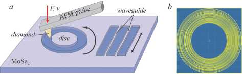
Fig. 1. (a) Scheme of the frictional scanning probe lithography method. AFM probe is repeatedly moved with a rate (ν) in a contact mode with a pressure force (F) according to the vectoral lithographic pattern. (b) Example of the vectoral lithographic pattern for the creation of the microdisk optical cavity. Yellow circles indicate places where the material will be removed
Results and discussion
Fig. 2 a and c present the AFM images of the GaP and MoSe 2 microdisks carved from the GaP layer deposited on sapphire and the MoSe2 flake on SiO2. The pressure force during the f-SPL was 2 ^N, and the scanning rate ( v ) was 10 ^m/ sec. Increasing of the scanning rate for the circular templates leads to the distortion of the circular shape due to temporal features of the AFM feedback loop and the AFM scanner. The lithographic pattern from Fig. 1 b was repeated ten times, and this process was sufficient to remove a 200-nm-thick GaP layer. The microdisks are characterized by relatively smooth edges and are considered to be an effective optical resonator. It is unfortunate that GaP is an indirect semiconductor. Consequently, the quality factor of the GaP cavity cannot be estimated from the PL experiment.
The shape of the carved cavity exhibits a slight deviation from a perfect circular disk (Fig. 2 a ), a consequence of the probe's pyramid shape during the f-SPL processing of the relatively thick GaP layer. It has been demonstrated that pyramids possess edges with varying angles of inclination. During the circular movement of the probe (see arrow at the left side of Fig. 1 a ), the pressure force between the pyramid and the GaP layer will be azimuthally nonuniform, which will result in azimuthally nonuniform disk edges [19].
As illustrated in Fig. 2 b , the stripe waveguides have been carved from the GaP layer. The material removal process was executed through a scanning procedure of the rectangular area in a contact mode with a pressure force of 2 ^N, with a scanning rate ( v ) of 300 ^m/ sec. In this linear scanning mode, the scanning rate can be significantly increased without distortion of the line shape. The waveguides were 30 ^m in length, with a width ranging from 1 to 1.8 ^m. The waveguides exhibit a non-ideal shape due to the drift of the sample during the acquisition of an AFM image in contact mode. Fig. 2 d shows an optical image of MoSe 2 microdisks created on a 40 nm thick flake, which were studied by the PL.
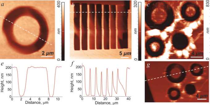
Fig. 2. Created by the f-SPL photonics units. AFM images (a, b, g) and the corresponding profiles (e, f, h) along the dashed lines. (a) AFM image of the GaP microdisk cavity. (b) AFM image of the GaP stripe waveguides (light stripes between dark nanogrooves).
AFM image of the MoSe 2 microdisk cavities (c) after the carving and (g) obtained during the cleaning (the right lower microdisk is shifted outside the scanning area by the probe). (d) Optical image of the MoSe 2 disk cavities carved from the 40 nm-thick flake
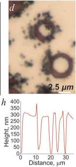
As illustrated in the Fig. 2 c – d , the removed material is dispersed throughout the processed area during the carving process. This phenomenon is particularly evident in the upper microdisk (Fig. 2 d ). The microdisk surface was cleaned by means of a scanning procedure in a contact mode subsequent to the carving. It is important to acknowledge that the DRP_IN cantilevers exhibit a high stiffness level of approximately 100 N/m. Consequently, scanning in a contact mode will result in the disk's movement. The disk was properly cleaned using an additional cantilever with a stiffness of 0.5 N/m. The lower disk depicted in the figure has been cleaned, and the removed material has been swept to the left. Fig. 2 g shows an AFM image if the cleaned surface with mikrodisks presented in Fig 2 c . From the AFM image in Fig. 2 b and the corresponding profile in Fig. 2 f one can notice a nonuniform depth removal of the GaP material between the waveguides. Possible explanation of this nonuniformity is the inhomogeneous mechanical properties of the polycrystalline epitaxial GaP layer. AFM topography profiles in Fig. 2 e and 2 h illustrate a material removal with the depth of 200 nm for the 200 nm-thick GaP layer and 300 nm for the 300 nm-thick MoSe 2 flake, correspondingly.
Fig. 3 shows an PL spectrum obtained for the MoSe 2 microdisk from Fig. 2 d (lower). The spectrum shows a broad peak with a maximum at the 910 nm. This peak is consistent with the indirect exciton transitions observed in a bulk MoSe 2 [21]. It is noteworthy that the bulk TMD materials exhibit indirect bandgaps, resulting in low PL intensity. However, the Purcell effect, a phenomenon in which the spontaneous emission rate of a system is enhanced by the presence of an optical cavity, can lead to an enhancement of the PL (luminescence) by several orders of magnitude [21]. This effect can be further exploited to achieve lasing generation [25]. The broad spectrum is modulated by the narrow features, which can be attributed to the WGM modes.
In order to verify the presence of the WGMs in such a thin MoSe 2 disk, a modeling procedure was carried out in the COMSOL Multiphysics software. The calculation was performed using a circularly symmetrical model, with the geometry representing the experiment [18]. It is noteworthy that the MoSe2 exhibit a substantial optical anisotropy [8], with distinct and disparate refractive indexes in the in-plane ( n o ) and out-of-plane ( n e ) directions. Furthermore, the refractive indexes demonstrate a significant dispersion. To ensure the accuracy of the calculation, multiple values corresponding to various wavelengths were considered. For the 920-nm case, the values of n o and n e are 4.6 and 3.06, respectively, and the extinction coefficient, k, is 0.013. For the 980-nm case, the values of n o and n e are 4.45 and 3.06, respectively, and k is 0.004 [10]. The diameter of the disk was of 2.8 µm.
As a result of the calculation, the observed WGM features in Fig. 3 a were labeled by the corresponding azimuthal and radial numbers. The observation of modes with unity radial number was determined by their superior Q-factor. The calculated position of the modes exhibited a high degree of agreement with the experimental results, with a deviation of less than several nanometers.
In order to estimate the efficacy of the f-SPL in creating MoSe 2 microdisk cavities, a comparison was made between the experimental and theoretical Q-factors (see Fig. 3c ). The upper inset of the figure displays a differential PL spectrum subsequent to the subtraction of the broad PL peak measured on the pristine MoSe 2 flake. The experimental Q-factor was calculated as the mode peak center position divided by the full width at half maximum of the peak. As illustrated in
Fig. 3 c , it is evident that the experimental values are approaching a value of 100, indicating a significant discrepancy between the experimental and calculated values. This discrepancy may be explained by the underestimation of the extinction coefficient or by the non-ideal edges of the carved microdisk. However, the WS 2 microdisks fabricated using the same techniques exhibited Q-factors that closely aligned with the model predictions, attaining a value of 700 [18].
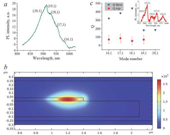
Fig. 3. (a) PL spectrum of the MoSe 2 microdisk cavity (lower disk shown in Fig. 2d). (b) Cross section of the axial symmetry model with a distribution of the square electrical field inside the MoSe 2 disk for the WGM with an azimuthal number of 19 and the unity radial number. (c) Experimental (red dots) and calculated (blue triangles) Q-factors of the observed WGM modes. Upper inset shows a PL spectrum obtained after the subtraction of the broad peak corresponding to the indirect exciton
It is noteworthy that the calculated Q-factor values are non-monotonically dependent on the azimuthal number. The phenomenon under observation can be explained by the equilibrium between the two effects. The initial phenomenon corresponds to an increase in extinction coefficient and material losses, as the mode number rises. The phenomenon of material losses is governed by the indirect exciton absorption. The second mechanism pertains to the enhancement of radial losses, which occur as the mode number of the disk, characterized by its relatively small diameter, rises.
Scanning probe lithography is conventionally criticized for the relatively low throughput, primarily due to its low scanning speed. However, this drawback can be overcome by using a parallel scanning in the many cantilever system and using a high-speed scanner [26]. In our particular case the AFM device was not specially optimized for the high throughput SPL and the probe moving speed was not exceed 300 μm/sec. Microdisk shown in Fig. 2 a was carved in 1 minute.
Conclusions
In summary, a frictional scanning probe lithography was successfully implemented to create microdisk cavities and stripe waveguides from a GaP layer that was grown on sapphire. The 30-micrometer-long and 1.5-micrometer-wide waveguides were demonstrated. The study of spectral features by means of microphotoluminescence was conducted using microdisk cavities that were carved from a 40-nm-thick MoSe 2 flake. The presence of whispering gallery modes was observed in the PL spectrum, with a quality factor that reached 100. Therefore, f-SPL can be implemented for the purpose of creating photonic circuit units.
Acknowledgements
The work is supported by Russian Science Foundation, 24-12-00209,