Групповые вычисления в неблокируемых системных сетях

Автор: Подлазов В.С.
Журнал: Программные системы: теория и приложения @programmnye-sistemy
Рубрика: Программное и аппаратное обеспечение распределенных и суперкомпьютерных систем
Статья в выпуске: 5 (68) т.16, 2025 года.
Бесплатный доступ
Рассмотрены неблокируемые оптоэлектронные сети, в которых выполняются групповые операции над множеством чисел за время передачи одного числа. Рассмотрено выполнение групповых операций исполнительными фотонными блоками, размещенными при каждом абоненте сети, и представлена схемотехника этих блоков. Исследована возможность выполнения групповых операции в циклических последовательностях узлов, задаваемых гамильтоновыми графами. Предложены процедуры построения этих циклических последовательностей и выполнения в них групповых операций. Рассмотрена возможность построения неблокируемой электронной системной сети на любое число абонентов. Предложен способ построения оптоэлектронной сети как тандемной сети, в которой оптоэлектронные переключатели управляются их аналогами из электронной сети.
Неблокируемые системные сети, групповые операции, фотонные и оптоэлектронные переключатели и коммутаторы, гамильтоновы циклы узлов сети, тандемные неблокируемые сети
Короткий адрес: https://sciup.org/143185288
IDR: 143185288 | УДК: 004.724.2+004.272.43 | DOI: 10.25209/2079-3316-2025-16-5-3-42
Group Computing in Non-blocking System Area Networks
This paper is devoted to non-blocking optoelectronic networks in which group operations over a set of numbers are executed during the transmission of one number. The execution of group operations by photonic units placed at each network user is considered, and the circuitry of these units is presented. The possibility of executing group operations in cyclic sequences of nodes defined by Hamilton graphs is investigated. Procedures for constructing such cyclic sequences and executing group operations in them are proposed. The possibility of designing a non-blocking electronic system area network for any number of users is studied. A method for designing an optoelectronic network as a tandem network with optoelectronic switches controlled by their analogs from the electronic network is described.
Текст научной статьи Групповые вычисления в неблокируемых системных сетях
In modern computing systems based on system area networks (SANs) being developed, data are transmitted together with commands, forming spatial data flow structures [1] . A particular case is computing systems with parallel data processing during their transmission in the network: a group operation over a set of numbers is executed while one number (the result of this operation) is transmitted via a common channel of the network. Such operations, called common channel computing (CCC) [2] , can be executed in direct channels without intermediate buffering (on-the-fly). The simplest examples of CCC operations are summing a set of numbers from different nodes or finding the maximum of them.
A channel is common if users can transmit signals into this channel in parallel with their overlapping, which can be used for group computations. A common channel is direct if it has only transmission delays of signals or their combination delays, without any clock delays. CCC operations can be executed in cyclic sequences of network nodes forming Hamilton graphs. In this case, CCC operations on non-intersecting graphs can be executed in parallel.
Each network node needs executive units for different CCC operations. They can be built in the element base of optical channel splitters in a purely photonic implementation (without electronic control of units) [3] . By assumption, first, network nodes have the capability to transmit/receive data to/from executive units by optical signals; second, executive units work only with these optical signals. Such units allow executing arithmetic and logical operations over numbers represented by optical signals without using special photonic arithmetic-logical units (ALUs).
Cyclic sequences of nodes with direct channels can be constructed in non-blocking SANs, which are conflict-free on arbitrary permutations of packets between nodes. In the element base of switches and channel splitters (multiplexers/demultiplexers), it is possible to design non- blocking SANs with direct channels of any size according to the number of network users [4 , 5] .
Based on the above properties, the objective of this paper is to develop a method for designing a non-blocking SAN that executes CCC operations on-the-fly over an arbitrary set of nodes under a photonic implementation of executive units.
The following tasks are solved to achieve the ob jective:
-
(1 ) selecting an appropriate method to change the values of bits in the channel based on their two-rail representation;
-
(2) selecting an appropriate element base for photonic executive units;
-
(3) developing basic elements for the photonic implementation of arbitrary logical functions;
-
(4 ) synchronizing the bitwise overlapping of numbers in a common channel;
-
(5) developing photonic units to execute CCC operations with numbers from different network nodes;
-
(6) developing a method to design a non-blocking SAN of arbitrary size in the elem ent base of switches and channel splitters of a given size;
-
(7) developing a method to execute group operations in a SAN by forming Hamilton loops of network nodes;
-
(8) developing a method to design a non-blocking photonic network as part of a tandem network in which photonic nodes are controlled by electronic nodes.
In Section 1, we present a method for building photonic CCC units and a circuitry for their implementation. Section 2 considers a method for designing non-blocking SANs with direct channels and forming Hamilton graphs in them, including a method for embedding CCC units. In Section 3, we describe a method for designing non-blocking optoelectronic networks with Mach–Zehnder interferometers as an application base for photonic executive units.
1. Distributed Arithmetic Based on Photonic Switches
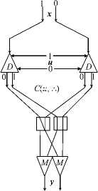
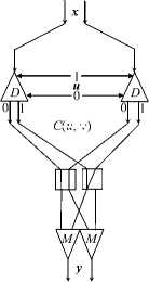
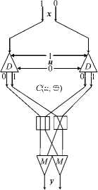
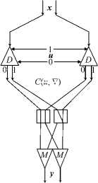
To execute CCC operations, logical variables are transmitted via the channel in the two-rail form (along two lines, 0 and 1). Value 0 is transmitted by a signal in line 0 in the absence of a signal in line 1, and value 1 is transmitted by a signal in line 1 in the absence of a signal in line 0. Lines 0 and 1 pass through the converter C i of each network node i. Each converter executes the unary operation O i of transforming an input logical variable x i to an output logical variable y i = O i x i .
The operation O i consists of the following transformations: repetition y i = x i (“=”), negation y i = — x i (“ — ”), change into the value y i = 0 (“0”), and change into the value y i = 1 (“1”).
C ( u , ∧ )
C ( u, л )
0 1 0 1
C ( u , ∨ )
C(u , v )
C ( u , ⊕ )
C(u , Ф )
1 0
C ( u , ∇ )
C ( u , V )
1 0
Figure 1. The circuits of logical functions from Table 1 for two-rail variables
Table 1. Logical functions by converter states for the adder
|
AND (logical conjunction) |
OR(logical disjunction) |
XOR(addition mod 2) |
Initial Run |
||||||||||||
|
ℵ = ∧ |
ℵ = ∨ |
ℵ = ⊕ |
ℵ = ∇ |
||||||||||||
|
x |
u |
O |
y |
x |
u |
O |
y |
x |
u |
O |
y |
x |
u |
O |
y |
|
0 |
0 |
«0» |
0 |
0 |
0 |
«=» |
0 |
0 |
0 |
«=» |
0 |
0 |
0 |
«=» |
0 |
|
0 |
1 |
«=» — |
0 |
0 |
1 |
«1» — |
1 |
0 |
1 |
«» — |
1 |
0 |
1 |
«0» — |
0 |
|
1 |
0 |
«0» |
0 |
1 |
0 |
«=» |
1 |
1 |
0 |
«=» |
1 |
1 |
0 |
«=» |
1 |
|
1 |
1 |
«=» |
1 |
1 |
1 |
«1» |
1 |
1 |
1 |
«» |
0 |
1 |
1 |
«0» |
0 |
The converter is used in four fixed states for which the operation O i is considered to be executed. Each state is defined by some configuration of a pair of fiber sections, given by the value of the two-rail control variable u i .
The circuits in Figure 1 show the use of such pairs of converters for implementing some logical functions on photonic demultiplexers D and multiplexers M for the two-rail variables x, u, and y .
For such circuits, we will follow the notation given at the bottom of Figure 1.
A photonic 1 x 2 demultiplexer D and a photonic 2 x 1 multiplexer M are used in Figure 1 . They are assembled from several thin-film layers of metamaterials with electro-optical or magneto-optical properties [6 , 7] . A peculiarity of these elements is that an optical signal is used to control switching. In the demultiplexer, they are converted into two control signals
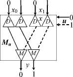
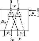
Figure 2. The circuits of a multiplexer and a demultiplexer for two-rail variables of an electronic or magnetic nature and supplied to a guide layer, which specifies two propagation directions for the information signal received at its optical input. As a result, the input optical signal is sent to one of the two optical outputs.
In this paper, one two-rail control variable is used; therefore, other single-layer devices with two outputs (demultiplexer) or inputs (multiplexer), such as gallium arsenide films [8] , can be selected. They allow building photonic logical elements directly controlled by light.
Table 1 provides the truth tables of the logical operations used in the circuits in Figure 1. Obviously, the operation ℵ is defined only by the pair of states of the converter C i , which are selected by the value of the variable u i . As a result, it is possible to execute the binary operation y i = x i ℵ u i (any of the sixteen logical operations) on a pair of the converters. Figure 2 also shows the circuits of a multiplexer (M u ) and demultiplexer (D u ) controlled by the variable u for two-rail variables.
When nodes are placed sequentially, it is possible to sum numbers at the nodes or select the maximum of them during the transmission of one number via the common channel. For this purpose, the numbers are transmitted as binary ones sequentially bitwise. To execute their addition, the numbers are transmitted with the least significant bits first; to find their maximum, with the most significant bits first.
In non-blocking SANs, there always exist cyclic sequences of nodes in the form of Hamilton graphs, and each such graph has a path passing through each node exactly once. This property directly follows from those of non-blocking networks ensuring conflict-free routing on arbitrary permutations of data packets. With the use of Hamilton loops, conflict-free data transmission is guaranteed and linear sequences of photonic units implementing group CCC operations are embedded in non-blocking networks. In this case, all data sources and sinks are defined.
---- [ Node 1 |
| Node 2 | x 21 si
U 2 (1)
;;H^ δ , ®)h —
P 2 i- 1
i
[ Nod e N ] ■■

- Ц С ( s i , V )| p 2 i
DL
δNi c (xN, л)
ε Ni
—* | С (AN , vf]
U N (1)
P Ni 1
• I M ( si ) I

■I С ( s i V )|
p Ni
DL
■I M ( s i )
y N ', y Ni
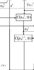
Figure 3. The N-node distributed adder
In each loop of nodes, an initial (first) node is separated to start the construction of the others (see the next section). This node triggers the command of the operation to be executed. For all nodes, the command sequentially synchronizes the start of executing a distributed operation r. At each node, there is a set of executive units, U (r), configured to execute individual operations. The operation command selects a particular executive unit. Each executive unit consists of circuits implementing the necessary logical operations in a definite sequence specified by their interconnections.
Figure 3 shows the units U 2 (1) and U N (1) at the second and N th nodes of the cyclic sequence that sum N numbers.
The initial first node of the network does not use its unit U 1 (1). It outputs slot X 1 , containing a binary multi-bit number starting from the least significant bits (on the two- rail value line), and slot S of the same bit length (on the two-rail synchronization line). In slot X 1 , the bits are transmitted by the variables x i 1 ; in slot S , by the variables s i , where i denotes the bit number. The first bit of slot S has value s 1 = 1 and the other bits s i = 0 for i > 1. The dots on the lines indicate the nodes of light signal separation by branching optical lines. The unit U 2 (1) of the distributed adder is connected to the first and second network nodes.
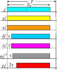
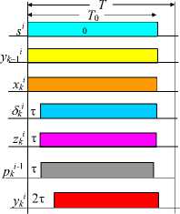
Figure 4. The timing diagram of the distributed adder
The circuits in Figure 3 are based on the well-known single-bit adder [9] , supplemented with a circuit to form the zero carry value from the previous bit for the first bit and a circuit to carry the value to the next bit through a one-bit delay line DL.
y.
Slots S , X 1 , and X 2 are supplied to the inputs of U 2 (1) synchronously bitwise; its output is slot Y 2 , containing the sum of numbers from slots X 1 and X 2 . In this unit, the values of the variables x i 1 and x i 2 are added mod 2 at the converter C (x ^ , ф ) to produce an intermediate result, i.e., the variable z 2 i . Together with the carry p i 2 -1 from the previous bit, the latter variable forms the output variable y 2 i of this bit at the converter C(p 2 , ф ) .
At the converter C(xl 2 , Л ), an intermediate variable 5 2 is obtained from the variables хг1 and x ^ . It is further used at the converter C (5 2 , Л ) to form the carry value p i 2 to the next bit. In turn, the last bit is generated from the intermediate variable ег2 obtained at the converter C(p - , Л ) from the result z 2 i and the carry value p i 2 - 1 from the previous bit.
The circuit C (s i , V ) forms the carry value from the previous bit for the first bit. The carry value in the first and other bits is passed through the multiplexer M (s i ).
Any kth node of the network (2
Figure 4 presents the timing diagram of the unit U 2 (1) in the first two bits with the following notations: T is the bit period; T 0 is the duration of active signals in it; τ is the time to tune the converter or multiplexer by the control variable u . Clearly, the output variable y 2 i appears in all bits
Node N i x N
y N –1 i
C ( x Ni , ∅ )
y Ni
si
zN– 1 i
#N– 1
U N (2)
s i
Figure 5. The N -node distributed maximizer
Table 2. Logical functions by converter states for the maximizer
Also, Figure 4 (left and right) shows the timing diagram of the units U 2 (1) and U k (1) of the distributed adder (in the same notation). Note that the right diagram is valid for any unit U k (1), k > 2. In other words, the output variable y k appears with a delay of 2т with respect to the beginning of the synchronization signals s i for any k and i (for any number of nodes and in all bits) and is given by signals of duration T 0 — 2т .
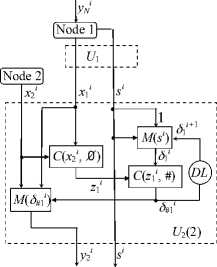
Along with the above CCC addition, the first node can also set the maximization operation (find the largest number of those placed at the network nodes). Following this command from the source node, an executive unit U k (2) (maximizer) is selected at each next node; see the circuit in Figure 5.
The units U k (2) also include circuits executing the logical functions from Table 2.
The first node of the network outputs to the unit U2(2) slot X1, containing a binary multi-bit number starting from the most significant bits (on the two-rail value line), and slot S of the same bit length (on the two-rail synchronization line). In slot X1, the bits are transmitted by the variables xi1 ; in slot S, by the variables si , where i denotes the bit number. The first bit of slot S has value 1 (s1 = 1) and the other bits are 0 (si = 0 for i > 1).
Any other node of the network (1 < k < N ) transmits to its unit U k (2) slot X k , containing the values of the variables x i k for each bit (on the value line). In addition, this unit receives slot S from the executive unit of the previous node.
Figure 5 (left) shows the circuit of the unit U 2 (2) connected to the first and second network nodes of the distributed maximizer. The dots indicate the nodes of light signal separation by branching optical lines. Optical signals can be attenuated using photonic amplifiers at the output of the units U k (2) [10] .
The variable J J must have the value 5 J = 1 for all bits i < j with x i > x 2 and the value J J =0 for all bits i > j (after the jth bit) with x j < x 2 . This value sequence of 5 1 is formed by the converters C (xl 2 , 0 ) and C (z J , #) together with the multiplexer M (s i ) and the one-bit delay line DL. The former converter generates the value of the intermediate variable z 1 i from those of the variables x i 1 and x i 2 , implementing logical switching (Table 2) for k > 2. The latter converter forms the value of the variable J i , implementing logical repetition ( Table 2) for k > 2. The multiplexer M (s i ) and the delay line DL produce the values of the variable 5 1+1 = J # 1 for the next bit.
For bits j < j with the value 5 J = 1 stored, the output variable y 2 = x J is obtained through the multiplexer M (5 # 1 ),. However, for bits j > j with the value 5 J = 0 stored, the output variable y 2 = x 2 is obtained through the multiplexer M (5 # 1 ). For the ith bit, the resulting value is y 2 = x j2 = 1.
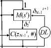
Figure 5 (right) presents the circuit of the unit U k (2), actually repeating for (k > 1) that of the unit U 2 (2) with x 1 replaced by y k-1 and 2 by k in the subscripts.
Figure 6 shows the timing diagram of forming different variables for the j th and (j + 1)th bits with the following notation: т is the tuning time of the converters and multiplexer; T and T 0 are the durations of the bit and the active signal in it. Obviously, the active signal is shortened by a time not exceeding 3т, which is independent of j.
Concluding section 1, note that the distributed photonic adder and maximizer can also be easily implemented in the electronic element base by replacing the delay line DL with a 1-bit shift register.
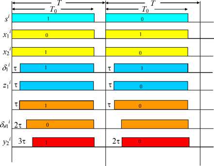
Figure 6. The timing diagram of the two-node maximizer for the jth bit
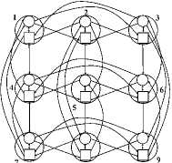
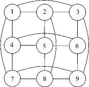
Figure 7. A two-dimensional ternary hypercube as a graph (left) and a digraph (right)
2. Hamilton Loops in Non-blocking System Area Networks
In section 2 we introduce non-blocking SANs as switches with the highest speed and complexity. Figures 7 –9 demonstrate principles for building non-blocking self-routing distributed switches. First (Figure 7, left), consider a two-dimensional m-ary hypercube as a graph. If processors and switches are distinguished at its nodes, the hypercube becomes a digraph (Figure 7, right), which can be represented in bipartite form as a quasicomplete digraph (Figure 8) . It can be built in the element base of m X m switches S o , 1 X m demultiplexers, and m X 1 multiplexers (Figure 9) , thereby forming the distributed switch S 1 (N 1 ,m). The latter is a self-routing and non-blocking switch on arbitrary permutations for N = m 2 users [4, 5] .
Connections in the switch S i (9, 3) are given by different incident tables
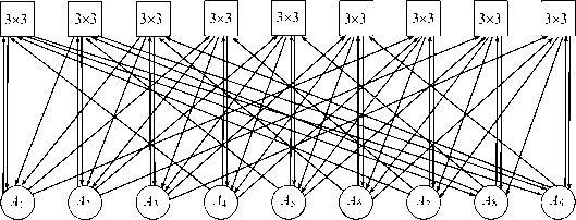
Figure 8. A quasicomplete digraph with m = 3
1 2 3456789
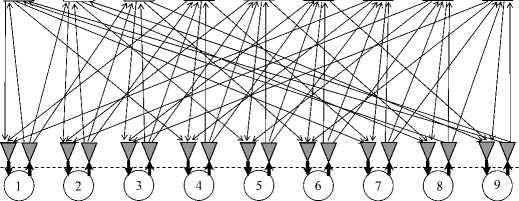
Figure 9. The switch S 1 (9, 3) with the quasicomplete digraph topology
Table 3. The incidence table for a quasicomplete digraph with m = 3
Table 4. The incidence table for a quasicomplete digraph with arbitrary m
|
Switches |
Channels from users |
Channels to users |
||||||
|
1 |
1 |
2 |
... |
m |
1 |
1 + m |
... |
1 + m(m — 1) |
|
2 |
1 |
2 |
... |
m |
2 |
2 + m |
... |
2 + m(m — 1) |
|
... |
1 |
2 |
... |
m |
... |
... |
... |
... |
|
m |
1 |
2 |
... |
m |
m |
m + m |
... |
m + m(m — 1) |
|
m + 1 |
m + 1 |
m + 2 |
... |
m + m |
1 |
1 + m |
... |
1 + m(m — 1) |
|
m + 2 |
m + 1 |
m + 2 |
... |
m + m |
2 |
2 + m |
... |
2 + m(m — 1) |
|
... |
m + 1 |
m + 2 |
... |
m + m |
... |
... |
... |
... |
|
m + m |
m + 1 |
m + 2 |
... |
m + m |
m |
m + m |
... |
m + m(m — 1) |
|
... |
... |
... |
... |
... |
... |
... |
... |
... |
|
m 2 — m + 1 |
m 2 — m + 1 |
m 2 — m + 2 |
... |
m 2 |
1 |
1 + m |
... |
1 + m(m — 1) |
|
... |
m 2 — m + 1 |
m 2 — m + 2 |
... |
m 2 |
2 |
2 + m |
... |
2 + m(m — 1) |
|
m 2 — 1 |
m 2 — m + 1 |
m 2 — m + 2 |
... |
m 2 |
... |
... |
... |
... |
|
m 2 |
m 2 — m + 1 |
m 2 — m + 2 |
... |
m 2 |
m |
m + m |
... |
m + m(m — 1) |
14 Viktor S. Podlazov EN RU
Table 5. The incidence table for the non-blocking switch 5 2 (27, 3)
|
K 1 (9,3) |
From users |
To users |
||||||||||||||||
|
1 |
1 |
2 |
3 |
10 |
11 |
12 |
19 |
20 |
21 |
1 |
4 |
7 |
10 |
13 |
16 |
19 |
22 |
25 |
|
2 |
1 |
2 |
3 |
10 |
11 |
12 |
19 |
20 |
21 |
2 |
5 |
8 |
11 |
14 |
17 |
20 |
23 |
26 |
|
3 |
1 |
2 |
3 |
10 |
11 |
12 |
19 |
20 |
21 |
3 |
6 |
9 |
12 |
15 |
18 |
21 |
24 |
27 |
|
4 |
4 |
5 |
6 |
13 |
14 |
15 |
22 |
23 |
24 |
1 |
4 |
7 |
10 |
13 |
16 |
19 |
22 |
25 |
|
5 |
4 |
5 |
6 |
13 |
14 |
15 |
22 |
23 |
24 |
2 |
5 |
8 |
11 |
14 |
17 |
20 |
23 |
26 |
|
6 |
4 |
5 |
6 |
13 |
14 |
15 |
22 |
23 |
24 |
3 |
6 |
9 |
12 |
15 |
18 |
21 |
24 |
27 |
|
7 |
7 |
8 |
9 |
16 |
17 |
18 |
25 |
26 |
27 |
1 |
4 |
7 |
10 |
13 |
16 |
19 |
22 |
25 |
|
8 |
7 |
8 |
9 |
16 |
17 |
18 |
25 |
26 |
27 |
2 |
5 |
8 |
11 |
14 |
17 |
20 |
23 |
26 |
|
9 |
7 |
8 |
9 |
16 |
17 |
18 |
25 |
26 |
27 |
3 |
6 |
9 |
12 |
15 |
18 |
21 |
24 |
27 |
Routing in the switch S 1 (N 1 ,m) is performed using the wormhole technique, i.e., by the output port numbers of the demultiplexer and switch.
With the internal scaling method [11] , the non-blocking switch S i+ 1 (N i+ 1 ,m) with N i +1 = m i +1 can be built from several non-blocking switches S i (N i ,m). More precisely, the switch S i +1 (N i +1 ,m) is obtained from N 1 switches S i (N i , m) and a layer of N i +1 couples of 1 x m demultiplexer and m x 1 multiplexer. Each switch S i (N i , m) is divided into parts of m ports; in each part, a separate switch S i (N i , m) is constructed from all switches with initial numbering in each part and end-to- end numbering across all parts.
Table 5 provides an example of the incidence table of a switch S 2 (27, 3) from the incidence tables of switches S 1 (9, 3).
The connections in the switch S i+ 1 (N i + 1 ,m) are constructed as follows. According to the source and sink numbers given, the switch S i (N i ,m) with both numbers (from the source and to the sink) is searched in the incidence table. The connection between the users is routed through the selected switch. For example, in Table 5 , source 2 and sink 23 are connected through the switch with number 2.
Routing in the switch S i (N i , m) is performed using the wormhole technique, i.e., by the output port numbers of the demultiplexers from the sources and further by the port numbers in switches S i-1 (N i-1 ,m').
The switch S i (N i , m) has the complexity C i , expressed in the number of switching points; see formula (1) . The number of channels in this switch, 3
L 1 = 2N j 2 , is significantly smaller than in the complete graph.
C 1 = 2(m 4 + m 3 ) = 2(N 2 + N - 3 )
(1) 3
L 1 = 2m 3 = 2N 1 2
The complexity and number of channels in the switch S i (N i ,m) are given by the recurrence relations C i = C i - i N i + 2mN i and L i = L i-1 N 1 + 2mN i . After straightforward transformations, we obtain the complexity and number of channels described by the formulas
|
2( i +1) 2( i +1) k S i = 2 ^ m k = 2 ^ N i i +1 |
|
|
(2) |
k=i+2 k=i+2 2 i +1 2 i +1 k L i =2 ^ m k = 2 ^ N i i +1 k=i+2 k=i+2 |
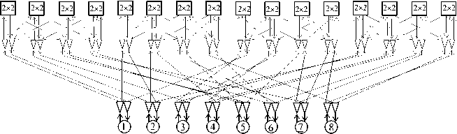
In non-blocking switches S i (N i ,m), it is possible to construct nonintersecting cyclic sequences of users (Hamilton graphs) with direct channels and completely defined nodes with initial data and the result. They are created by the sequential transmission of packets with intermediate sink addresses (in the form of packets of output port numbers) by the source nodes, with fixing the connections made.
As an illustrative example, Table 6 gives the incidence table of the switch S 2 (8, 2), and Figure 10 shows its circuit with two non-intersecting sequences of users. In this circuit, the connections for sequences 1-6-3-8-1 and 7-2-5-4-7 are highlighted in color, including initial users 1 and 7 creating them. The sequences are conflict-free by channels, and transmissions in them can be performed independently and in parallel.
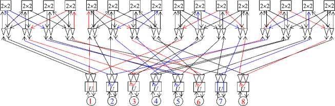
Between each user and its channel splitters, it is possible to insert the executive unit U of the CCC operation from Section 1 (in the electronic version, see Figure 11) . In the resulting SAN, different CCC operations can
Table 6. The inciden b the non-b itch
S 2 (8, 2) obtained from the switch S i (4,2)
|
Si (4, 2) |
From the source |
To the sink |
||||||
|
1 |
1 |
2 |
5 |
6 |
3 |
5 |
7 |
10 |
|
2 |
1 |
2 |
5 |
6 |
4 |
6 |
8 |
20 |
|
3 |
4 |
7 |
8 |
3 |
7 |
5 |
3 |
30 |
|
4 |
3 |
4 |
7 |
8 |
2 |
8 |
6 |
40 |
2 X 2
Figure 10. The switch S 2 (8, 2) with cyclic sequences 1-6-3-8-1 and 7-2-5-4-7
1-6-3-8-1, 7-2-5-4-7
Figure 11. The switch S 2 (8, 2) with executive nodes for
CCC operations be executed in cyclic sequences of nodes independently. The source nodes construct these cyclic sequences and set particular operations in them and, moreover, synchronize their execution (see section 1).
We compare the execution time of the group addition operation of numbers placed at N nodes of the networks similar to those in Figures 10 and 11.
In the first network, addition is executed by steps on a binary tree. The first step is to add, in parallel, the pairs of initial numbers at neighbor nodes, yielding N/2 intermediate sums of this step. At the ith step (1 < i < log 2 N ), the parallel addition of the intermediate sums of the (i — 1)th step is executed.
Let us introduce the following notation: T num is the time for transmitting a number to the network; τ is the average time for transmitting a number through the network to a neighbor node; δ is the time for executing addition at a node. Then the average addition time is given by
° = (T num + 5 ) log 2 N + T (1+2+ • • • + N/2)+ T = (T num + 5) log 2 N + TN.
A Hamilton loop of nodes is formed in the time
W = N(T + Tadd)+ Tcode, where Tadd is the time for transmitting an address to the network and Tcode is the time for transmitting the code of an operation under execution. Then the total time of the addition operation is
S = ° + W = (T num + 5) log 2 N +2TN + NT add + T code .
In the second network, the addition time (CCC operation) is given by
0 = Nt + NT add + T code + T num .
As a matter of fact, it includes the formation time of a Hamilton loop of nodes. Indeed, the CCC operation is executed on the trailing edge of the transmission of the operation code immediately after the transmission of the address packet for forming the Hamilton loop; hence, the additional transmission time over the network τ is not required here.
Obviously, S > 20. Note that the first operation is executed with program control of its steps whereas the second one is executed entirely in hardware, which even strengthens the above inequality.
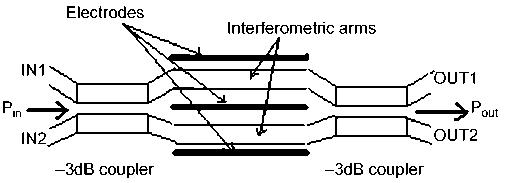
Figure 12. The switch 5 2 (8, 2) with executive nodes for
CCC operations
3. Non-blocking System Area Networks from Optoelectronic Switches Based on Mach–Zehnder Interferometers
An optical network for CCC can be built from optoelectronic switches based on Mach-Zehnder interferometers (MZI) [12 , 13] . A conventional 2 x 2 MZI switch involving electrooptical properties (a passive EO-MZI structure) consists of two equal-length interferometric arms connected between two couplers; see Figure 12.
It operates as follows: the first coupler is used to uniformly split light into two parts, which experience a net phase change of 2∆ϕ while passing through the interferometric arms. This phase difference is due to the pull-push effect of the field applied in opposite directions through the waveguides under the electrodes. As discovered for this structure, the output intensity is periodic with minima and maxima occurring at odd and even integer multiples of the voltage applied.
Therefore, light can be produced at the output ports through constructive or destructive interference phenomena. When the phase difference between the two arms is appropriately accumulated, it causes the appearance of recombined light in one of the output arms (i.e., the function of an optical 1 x 2 demultiplexer is realized).
Such switches can be used to assemble an optoelectronic 4 x 4 switch [13] with data transmission by optical signals and electronic control by a network node. Currently, the speed of such switches reaches up to 100 Gbps [14] and they have a fairly high packing density [15].
A non-blocking optical network can be based on tandem switching devices consisting of similar electronic and optoelectronic components. The former are involved in routing and route fixing as well as set the configuration of the latter. Tandem switching devices should have an identical configuration and operate in the master-slave mode for electronics and optics, respectively. The resulting non-blocking tandem network consists of copies of electronic and optoelectronic networks.
At the inputs/outputs of the second network, it is possible to place photonic executive nodes (Section 1) to execute CCC operations with higher speed and higher noise immunity.
Conclusion
In this paper, we have considered a method and circuitry for building non-blocking system area networks (SANs) to execute group operations in Hamilton loops of network nodes. Group operations are executed as common channel computing (CCC) operations with the highest speed. The SANs can have electronic and optoelectronic (tandem) implementation. The executive units of CCC operations can have both electronic and photonic implementation.
Note that the purely photonic implementation of executive units is one of the four innovations of this paper. The second innovation is the internal scaling method for non-blocking SANs with the digraph structure. The third one is a way to embed group operation circuits into a non-blocking SAN through the use of Hamilton loops. Finally, an innovation is the tandem method for organizing an optoelectronic non-blocking network.
