Hardware Design and Simulation of Sobel Edge Detection Algorithm

Author: Sohag Kabir, A S M Ashraful Alam
Journal: International Journal of Image, Graphics and Signal Processing(IJIGSP) @ijigsp
Article in issue: 5 vol.6, 2014.
Free access
In this paper, a hardware system for Sobel Edge Detection Algorithm is designed and simulated for a 128 pixel, 8-bit monochrome line-scan camera. The system is designed to detect objects as they move along a conveyor belt in a manufacturing environment, the camera will observe dark objects on a light conveyor belt. The edge detector is required to detect horizontal and vertical edges using Sobel edge detection method. The Sobel operator requires 3 lines and takes 3 pixels per line, thus using a 3×3 input block to process each pixel. The centre pixel of the 3×3 pixel block can be classified as an edge point or otherwise by thresholding the value from the operator. The FPGA based Sobel edge detector is designed and simulated using Altera Quartus II 8.1 web edition by targeting Cyclone II development boards.
Edge detection, Sobel Edge detection, Image Processing, FPGA, Hardware Design, Simulation
Short address: https://sciup.org/15013291
IDR: 15013291
Text of the scientific article Hardware Design and Simulation of Sobel Edge Detection Algorithm
Published Online April 2014 in MECS DOI: 10.5815/ijigsp.2014.05.02
Edge detection is the process that efforts to define significant variations of the intensity level in the image with regards to the physical events that have originated them [1, 2]. The objective of discovering distinct changes in the brightness of image is to capture important activities and changes in the entities of the image. Application of an edge detection algorithm to an image may considerably decrease the amount of details to be processed and therefore narrow out details that may be considered as less appropriate without changing any important properties of the image. Most frequently used edge detection methods are Roberts Detection, Prewitt Detection, Sobel Detection, and Canny Detection [3-6] and software implementation of these methods are available. Software versions are suitable for general purpose use but their processing speed may not be able to fulfill the demand of real-time environment operation where a large amount of information is required to be processed in a short period of time i.e. throughput is higher. FPGA based application-specific hardware design can provide higher processing speed over their equivalent software versions by utilising the advantage of highly parallel nature of their architecture.
In this work, Sobel edge detection algorithm is implemented in hardware as a part of line-scan edge detector which is shown in Fig.1[7]. Line-scan edge detector consists of different modules but this paper mainly concentrates on Sobel Analysis module. In order for the line-scan edge detector to operate and function correctly, there are several specific requirements the system will need to meet:
-
• Controlled data flow between line-scan camera, ADC, auto-calibration and edge detector circuit.
-
• Select a suitable ADC circuit which is capable of converting the analogue camera data to 8-bit pixel data, ready for the Sobel edge detector circuit to analyse the pixels.
-
• The circuit must be capable of auto-calibrating when initiated from an external command, which will set the exposure of the line-scan camera. This is required as the camera will need to detect the difference between the light background and the dark objects.
-
• The circuit will to store 3 lines of data from the ADC, which will then be used in the Sobel edge detector.
-
• The edge detection circuit will calculate horizontal and vertical object edges, using Sobel edge detection method.
-
• Once the edges have been detected the data will be encoded to determine the status of each pixel. The encoded output will be a 2 byte output, byte 1 will contain the encoded data and byte 2 will contain the run length data. Whenever any bit in byte 1 changes a new byte pair will be outputted.
-
• The encoded data is then compress, using run length encoding. Whenever any bit in byte 1 changes the compressed data will be sent to the memory buffer, this then allows a microprocessor to read the data, without having synchronized clock signals.
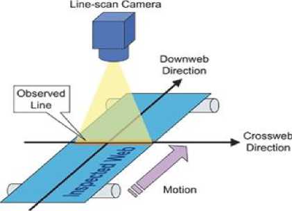
Figure 1.Line-Scan Imaging System
Among different modules of line-scan edge detector system, the Sobel edge detector module performs the essential task by detecting the edges of the image taken by line-scan camera. As the Sobel edge detection module performs all its operation on digital data therefore it is considered that digital information of the image taken in conveyor belt is available for operation. Details of analogue to digital conversion of images taken by linescan camera are omitted here for simplicity. It is considered that the main memory of the line scan edge detector system store 3 lines of data (128 bytes/line) received from the ADC. The Sobel operator requires 3 lines and takes 3 pixels per line, thus using a 3×3 input block to process each pixel. All the necessary data for edge detection operation in Sobel edge detection module are provided by the main memory. When 3×3 input blocks of pixel information are provided as input to Sobel edge detector simultaneously from main memory then the Sobel edge detector performs necessary operation to evaluate Sobel edge detection algorithm to detect edges in X and Y direction.
The remainder of the paper is organized as follows. In section II, an overview of line-scan edge detector and necessary conditions to successfully implement Sobel edge detection algorithm in hardware is presented. Section III describes the specifications of Line-scan Camera and Analogue to Digital Converter (ADC). The Sobel edge detection method is described in Section IV. After that, hardware architecture and circuit design of Sobel edge detector is shown and discussed in section V. Section VI shows the operation and simulation result of Sobel edge detection module. Result and discussion are provided in section VII and finally, concluding remarks are presented in Section VIII.
-
II. LINE-SCAN EDGE DETECTOR OVERVIEW AND TIMING DIAGRAM
Fig. 2 below shows the bare-bones system design for the 8-bit monochrome line-scan camera and edge detector. The camera scans across a 128 pixel wide upon a light background. The data for each pixel collected from the camera is encoded by an ADC and passes the 8-bit digital output to the edge detection integrated circuit.
The timing diagram is necessary in order to understand the requirements of the line-scan camera. There are three main signals in the timing diagram below (Fig. 3) for the LVDS slave mode e.g. Line Transfer (LT), Line Enable (LEN) and camera clock (CCLK).
When the rising edge signal is detected by the Line Transfer (LT) input, the charge from each photo site will be transferred to the readout register; afterwards the readout register transports the charge from each photo site to the video outputs. While the Line Enable (LEN) signal is responsible for the valid digital video[8].
There are some requirements to operate the line-scan camera. For the LT signal, the minimum pulse duration of high-level must be more than 2 clock cycle and the minimum pulse duration of low-level pulse must be more than 6 clock cycle. While the LEN signal, the pulse will be initiated provided the period of 71(in worst case) clock cycles apart from the falling edge of the LT to the rising-edge of LEN, (see Fig. 3).
Therefore, the minimum clock cycle from time (a) where LT has been initiated to time (b) when the ADC receives the analogue video is 74 clock cycle. If the clock applied is 4MHz, the time spent is 18.5µs. The ADC latency time plus the total time for the ADC to read the analogue video will be the total time spent for edge detector to read the first pixel e.g. 18.533µs (latency time for selected ADC = 33ns).
The total time to convert the first line (128pixels):
73 minimum clock cycles + 128 clock cycles = 201 clock cycles
Total time = [201 clock cycles* time per clock cycle] + ADC latency time = [201 clock cycles* (1/4MHz)] + 33ns = 50.283µs
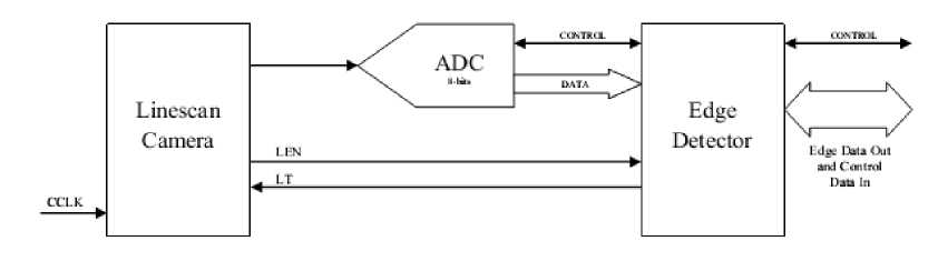
Figure 2.Edge detector connected to camera and external ADC
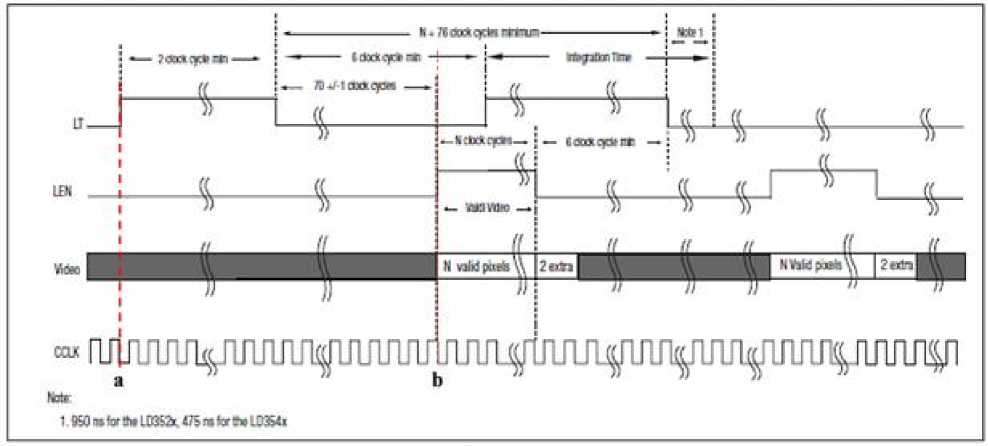
Figure 3.Camera waveforms in LVDS slave mode [9]
-
III. SPECIFICATIONS OF LINE-SCAN CAMERA AND PROPERTIES OF ADC
In order to convert the analogue output signal from the line-scan camera into digital form, an ADC is required. The specification of the camera needs to be considered when selecting an appropriate ADC. The working frequency of the ADC is determined by the camera. According to the reference information, the camera is working in LVDS slave mode (RS-644). In this mode, an optional Master Clock (MCLK) is provided to set the data rate frequency from 2MHz to maximum frequency which is defined by the internal oscillator. If there is no MCLK the camera will operate at its maximum frequency.
In addition, the LD3500 series have 2 typical maximum output rate (20MHz and 40MHz). Specification of LD3500 camera is shown in Table I [9].
Because LVDS mode is applied in LD35XXPGL-011 series, the maximum output rate is 20MHz. However, in practice the output rate is set at 4MHz. Therefore the ADC must be able to sample the data at 4MHz. ADC0804s030/040/050 is a series 8-bit Analogue-to-Digital Converter, it has a maximum sampling rate of up to 30, 40 and 50MHz respectively and a conversion time of one clock cycle.
TABLE I. LD3500 CAMERA SPECIFICATION
|
Camera Characteristics |
Value |
Camera Characteristics |
Value |
|
Number of Active Pixels |
512, 1024, or 2048 |
Adjustable Gain Range |
0 to 24.5dB(LD35xxPGK-011) 1,2,4,8X(LD352xPGL-011) |
|
Pixel Size |
14 im*14 цт |
PRNU |
+/- 10% |
|
Spectral Response |
250-1000 nm |
Dynamic Range |
250:1 |
|
Sensor Window |
Glass |
Maximum Output Rate |
20 MHz(LD352xPGx-011) 40 MHz(LD354xPGK-011) |
|
Exposure Control |
Yes |
Lens Mount |
U Mount |
|
Antiblooming |
Yes |
Operating Temperature |
-22° C to 55° C |
|
Number of Outputs |
1 |
Storage Temperature |
-40° C to 80° C |
|
Communications Protocol |
CameraLink(LD35xxPGK-011) ParallelLVDS(LD35xxPGL-011) |
Input Voltage |
12 to 24 VDC |
|
Output Depth |
8 bit |
TABLE II. DELAY TIME OF THE ADC0804S [11]
|
Conditions |
Min |
Typical |
Max |
|
|
Sampling Delay Time |
- |
3ns |
- |
|
|
Output Delay Time |
Vcco=4.75V |
- |
10ns |
13ns |
|
Vcco=3.15V |
- |
12ns |
15ns |
TABLE III. ADC COMPARISON (PRICES ARE CAPTURED FROM FUTURE ELECTRONICS [12] AND RS [13])
|
Name |
EN OB(bits) fin at 4.43MHz |
Sampling rate clock frequency (MHz) |
Power dissipation (W) |
Price/Piece(£) |
Conversion Time |
|
ADC 0804S030 |
7.8 |
30 |
175 |
1.55 |
One clock cycle 33ns |
|
ADC 0804S040 |
7.8 |
40 |
175 |
1.60 |
One clock cycle 25ns |
|
ADC 0804S050 |
7.8 |
50 |
175 |
1.71 |
One clock cycle 20ns |
|
ADC1175 |
7.3 |
20 |
60 |
7 |
50ns(20MHz) |
Total working timing of the ADC = sampling period + conversion time + output delay
Conversion time is one clock cycle and Output delay = 10ns (Vcco at 4.75V)
Conversion time = 1/30MHz = 33ns
Conversion time = 1/40MHz = 25ns
Conversion time = 1/50MHz = 20ns
Total working timing is:
30MHz ADC = 3ns + 33ns + 10ns = 46ns
40MHz ADC = 3ns + 25ns + 10ns = 38ns
50MHz ADC = 3ns + 20ns + 10ns = 33ns
ADC1175 is a single channel 8-bit ADC with a maximum sampling frequency at 20MHz[10].The typical conversion time is 20MHz, therefore for a single conversion it takes 50ns. In addition, it has a minimum conversion rate of 1MHz. Table III above shows the varying performance of the different ADC devices. As a conclusion, the ADC0804S series have a higher effective number of bits (ENOB) and are a much cheaper device. Although the power dissipation of ADC0804s is 3 times larger than that of ADC1175, the conversion time is shorter. In order to get the lowest conversion time, the ADC0804s050 is selected.
-
IV. SOBEL EDGE DETECTION METHOD
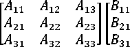
Sobel analysis is a technique used in image processing as a method for edge detection. The method calculates the approximate gradient of the image intensity at each point of an image by convolution with an integer value filter. The calculated gradient value allows the direction of the largest increase of light to dark and the rate of change in direction when comparing point values. This detail allows the edge to be identified by how abruptly or smoothly the image changes from point to point. Following equation is used for the convolution operation of the Sobel Edge Detection method [14].
В12
В 22
В 32
В13
В 23
В 33
] =∑( ^тп × ^тп )
where ^тп represents pixel information of the image and ^тп represents convolution mask for Sobel operator.
Different convolution masks are used for horizontal and vertical edge detection in Sobel edge detection method[15].Sobel operator mask for horizontal and vertical edge detection are given as:
1 0 -1 1 21
∆X=[2 0 -2] and ∆У=[0 00
1 0 -1 -1 -2-1
Equation for horizontal gradient calculation can be written as:
[
A11
A21
A31
A12
A22
A32
A13
A23
A33
1 0-1
]×[2 0-2]
1 0-1
=(A11+(2×A21)+A31)-(A13+(2×A23)+A33)
In the same way, equation for vertical gradient calculation can be written as:
[
A11
A21
A31
A12
A22
A32
A13
A23
A33
]×[
-2
' ]=(A11+(2×A12)+A13)-(A31+(2×A32)+A33)
The Sobel analysis module performs the edge detection operation of Line-Scan Edge Detector. The 9 bytes of pixel data from main memory are inputted into the Sobel module simultaneously, where the module performs all necessary calculations to evaluate the Sobel edge detection algorithm. At first it calculates the gradient values G SUM and G уSUM for X and Y directions respectively. Comparing these values with a threshold value, the module can make decision about the presence and absence of edge. After making decisions about the edges in X and Y direction, the decisions are outputted as G and Gу for X and Y direction edge respectively. The process for implementing Sobel edge detection operation in hardware is given below.
Sobel Edge Detection Operation in Hardware
Input: A sample image, enable signal and threshold value. Output: Detected edges in X and Y direction (G and Gу).
Procedure:
Step 1: Take 9 bytes pixel data from main memory.
Step 2: Apply Sobel masks to the input pixels.
Step 3: Apply Sobel edge detection algorithm to calculate gradients in X (G SUM) and Y (GуSUM) direction.
Step 4: If gradient in X direction; G SUM≥ threshold then output edge in X direction otherwise no edge in X direction.
Step 5: If gradient in Y direction; GуSUM≥ threshold then output edge in Y direction otherwise no edge in Y direction.
Step 6: Repeat Step 1 to 5 until all the pixels of the image is processed.
-
V. ARCHITECTURE OF SOBEL EDGE DETECTOR
The line-scan edge detector system has different modules and among those modules the edge detector module performs edge detection operation by implementing Sobel edge detection algorithm. The edge detector module along with other modules is shown in Fig.4.
Fig.5 below shows the block diagram for the Sobel analysis module; it details how the main memory data will be used in different calculation. The control module controls the operation of the Sobel module by sending a signal called SOB_CLK. It works like an enable signal for the Sobel module.
The G SUM and G SUM are calculated in the same arithmetic way, although the input pixels are different for X and Y direction gradient. Fig.5 shows how the G SUM andGуSUM are calculated by using subtractor, multiplier and adder. The multiplication of a number by 2 is performed by the left shift operation. This is achieved by proper wiring of bits of the number. To produce G and G у, comparators are used to compare the GSUM and GуSUM with threshold value.
It is seen from Fig.5 that the Sobel module consists of six full subtractors, four full adders, 2 multipliers and two comparators. It is required to design hardware for all functional components of the Sobel module and then integrate those components together to construct the whole module. In this paper, hardware for edge detector module is designed and simulated using Altera Quartus II software.
At first, circuit for a 1-bit full subtractor is constructed as a part of constructing subtractor module of the Sobel edge detector. The SOB_CLK enable signal is ANDed together with the inputs therefore when the enable is high normal subtraction operation is performed otherwise zero is generated as output irrespective to inputs. After creating block of 1-bit full subtractor, 8 of those are integrated together to make an 8-bit full subtractor as required by the system. After that, 8-bit full adder is constructed in the similar way as the full subtractor. For the operation of the Sobel analysis module a multiplier is required to multiply a number by 2. Multiplication by 2 is performed using the concept of left shift operation and it is done by careful wiring of bits of a number without using an extra module for multiplication operation. After calculating GSUM and GуSUM, it is required to check whether these values are greater than or equal to the threshold value. Therefore a comparator is designed in a way so that when input А ≥ input В then a logic high output is generated; otherwise a logic low output is generated.
After constructing and verifying the operations of all the smallest functional components, they are integrated together to construct the whole Sobel Edge detection module. All the smallest components are simulated using Altera Quartus II 8.1 web edition and it is seen that they are producing the expected results.
-
VI. Operation and Simulation Of Sobel Edge Detector
The main memory stores the pixel information of different lines of the image. To perform operation, the Sobel analysis module requires 9-bytes of pixel information. These 9-bytes are taken from 3 lines of pixel information that means 3-bytes per line. These data are provided to the Sobel analysis module by the main memory. How the information are stored in the main memory and feed to the Sobel analysis module is shown in Fig.6.
When 9 bytes pixel data is provided to the Sobel analysis module then two scenarios can occur. In the first scenario, the Sobel module is enabled for operation by high SOB_CLK(enable) signal which comes from control module.
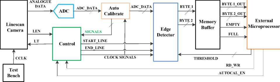
Figure 4. Block diagram of line-scan edge detector.
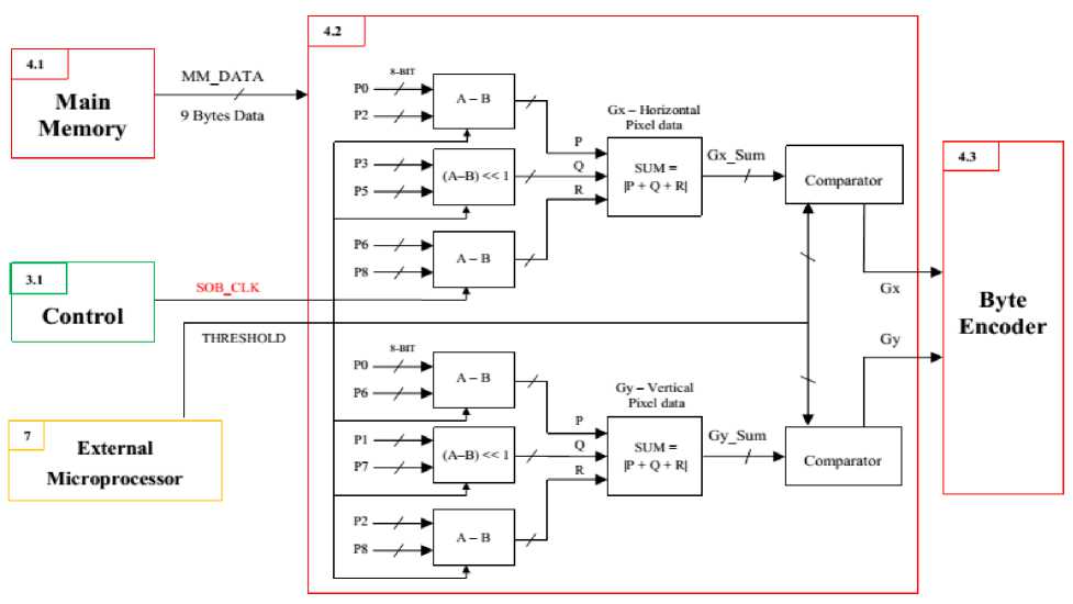
Figure 5. Block diagram of Sobel edge detector.
In this case, all the required values are calculated to find the values of gradient in X and Y direction. Sobel module calculates X and Y direction gradient using following equations.
X direction gradient,
G SUM=(P)-Р2)+(P5-Р3)+2(P3 -Р) (4)
Y direction gradient,
GуSUM=(P)-Р5)+(P2 -Р3)+2(PL-Р7) (5)
After calculating GSUM and GуSUM , the module compares these values with predefined threshold value. If these values are greater than or equal to the threshold value then the module can come to a decision that there is an edge in both X and Y direction. If any or both of the value are less than the threshold then the module decides that there is no edge on that particular direction.
As the Sobel module is unaware about the input bytes therefore it has to perform calculation on different data sets provided by the main memory in different time instances. The correctness of the Sobel edge detection module is verified by simulating the design using Altera Quartus II software and it is seen that the hardware model produces the same output as the software version. Fig.7 shows a small instance of the simulation output of the Sobel module with high SOB_CLK (enable) signal.
|
РО |
Р1 |
Р2 ... < Line 1 |
|
РЗ |
Р4 |
Р5 ... < Line 2 |
|
Р6 |
Р7 |
P8J ••• *___ Linc3 |
Figure 6. Stored pixel information structure in main memory
IV.U из
Instance 4: Both GXSUM(9C) and GySUM(M^ are greater than threshold (81) therefore Gx = 1 and Gy = 1.
Instance I: Both GxS(/Af(6C) and GySUM(2C) arc less than threshold (81) therefore G, = 0 and G„ = 0.
|
P0 |
Г 62 i |
BO x |
39 X |
r D4 ) |
p |
|||
|
Pl |
7E |
26 X |
9A X |
F7 |
} |
|||
|
P2 |
38 |
r--------------------- |
61 X |
31 X |
90 |
) |
||
|
P3 |
30 |
66 x |
ЗЕ X |
8A |
) |
|||
|
P5 |
25 |
_____39___________X_____ |
_36_________X. |
7F |
) |
|||
|
PG |
57 |
A9 X |
34 X |
05 |
) |
|||
|
P7 |
70 |
1D X |
38 X |
06 |
) |
|||
|
P8 |
2B |
65 X |
30 X |
77 |
) |
|||
|
SOB_CLK |
||||||||
|
GxSUM |
60 |
1 |
ED X |
IC x |
90 |
) |
||
|
GySUM |
2C |
U X |
D7 " Y |
84 |
) |
|||
|
THRESHOLD |
81 |
) |
||||||
|
Gx |
I________________________________Г |
|||||||
|
Gy |
___________________________________________________________________________I |
|||||||
Figure 7. Simulation of Sobel edge detector with high SOB_CLK (enable) signal
10.0 ns
40.0 ns!
Figure 8. Simulation of Sobel analyses with low SOB_CLK (enable) signal
In the second scenario, when a low SOB_CLK (enable) signal is sent to the Sobel module then the module produces low G and Gу output without considering the input of the module. Fig.8 above shows the simulation of the Sobel analysis module with low enable signal for 4 different sets of input at 4 different time instances. As the enable signal is low therefore the module produces zero as output irrespective to input.
-
VII. Result and Discussion
In The Sobel edge detection method calculates 2-D spatial gradient of an image intensity at each point of an image by convolution with an integer valued filter. The calculated gradient value allows the direction of the largest increase of light to dark and the rate of change in direction when comparing point values. This detail allows the edge to be identified by how abruptly or smoothly the image changes from point to point. To estimate gradient in X-direction (G ) and Y-direction (Gу), the method uses a pair of 3×3 convolution masks, one for each direction. Usually the actual image is much larger than the convolution mask as a result the mask slides over the image from left to right and top to bottom to process a square of pixels at a time. The mask start sliding over the image from left side of a row to estimate gradients for the central pixel of the overlapping area and then shifts one pixel to the right and continues until it reaches to the end of the row. When end of the row is encountered the operation starts again from the beginning of the next row and the operation continues until all the rows are processed. One important issue is that the pixels in the first and last row, as well as first and last column cannot be processed by using 3×3 convolution masks. The reason is that, when the 3×3 mask is placed over those specified position the mask will cross the boundary of the image. After estimating gradient in X and Y-direction ( G and Gу ) for each pixel, gradient magnitude at each pixel is calculated as:
G(x,y)=√(G)2+(Gу)2
Marking the pixel as edge point if G(x, y) ≥ т results the image of Fig. 9(b) from the original image of Fig. 9(a) where т is predefined threshold value.

(a) Input Image
Figure 9. Bird image Edge detection experimental result.

(b) Edge Detected Image
-
VIII. CONCLUSION
This paper mainly focuses on the design and simulation of a hardware system of the Sobel edge detection method. This method uses two 3×3 convolution masks to estimate gradient in X and Y-direction and which is easy to implement than other operators. The larger convolution masks of Sobel operator smoothed the image to a greater extent to make the operator less sensitive to noise. The Sobel edge detection method calculates 2-D spatial gradient of image intensity at each point of an image by convolution with small and integer valued filters therefore relatively less expensive in terms of computations. Application of Sobel edge detection algorithm to an image may considerably decrease the amount of details to be processed and therefore narrow out details that may be considered as less appropriate without changing any important properties of the image.
Sobel operator can be highly recommended in massive data communication considering the problems faced by interactive network users during massive image data transfer.
ACKNOWLEDGMENT
We would like to express our sincere appreciation and gratitude to Ian Bell at University of Hull, for his invaluable idea and encouragement to work on such an issue. We would like to thank Tim Shelley, Chine How Go and Dungeon Jin for their generous support, encouragement and friendship.
References Hardware Design and Simulation of Sobel Edge Detection Algorithm
- V. Torre and T. Poggio, “On Edge Detection,” IEEE Trans. Pattern Anal. Mach. Intell., vol. 8, no. 2, pp. 147–163, 1986.
- S. Tabbone and D. Ziou, “Edge Detection Techniques - An Overview,” Int. J. Pattern Recognit. Image Anal., vol. 8, pp. 537–539, 1998.
- N. Senthilkumaran and R. Rajesh, “Edge Detection Techniques for Image Segmentation – A Survey of Soft Computing Approaches,” Int. J. Recent Trends Eng., vol. 1, no. 2, pp. 250–254, 2009.
- M. Heath, S. Sarkar, T. Sanocki, and K. Bowyer, “Comparison of Edge Detectors: A Methodology and Initial Study,” Comput. Vis. Image Undersatnding, vol. 69, no. 1, pp. 38–54, 1998.
- R. Maini and H. Aggarwal, “Study and Comparison of Various Image Edge Detection Techniques,” Int. J. Image Process., vol. 3, no. 1, pp. 1–12, 2009.
- M. Sharifi, M. Fathy, and M. T. Mahmoudi, “A classified and comparative study of edge detection algorithms,” in Proceedings of International Conference on Information Technology: Coding and Computing, 2002, pp. 117–120.
- M. Huang, “Cover Image-PC-Based Line-Scan Imaging Systems,” ADLINK Technology Inc. [Online].Available:http://www.adlinktech.com/solution/tech_forum.php?file=measure/20050926.htm. [Accessed: 10-Sep-2012].
- “LD3500 Datasheet (PerkinElmer) - Low-cost Digital Linescan Camera, Automative Application.”[Online].Available:http://doc.chipfind.ru/perkinelmer/ld3500.htm. [Accessed: 25-Feb-2013].
- “LD3500 datasheet- PerkinElmer Optoelectronics - Low-Cost Digital Linescan Camera.” [Online]. Available:http://www.alldatasheet.com/datasheet-pdf/pdf/14895/PERKINELMER/LD3500.html. [Accessed: 07-Mar-2013].
- “ADC1175 Datasheet,” Texas Instruments. [Online].Available: http://www.ti.com/lit/ds /symlink/adc1175.pdf . [Accessed: 07-Apr-2013].
- “ADC0804S datasheet - NXP Semiconductors - Single 8 bits ADC.” [Online]. Available: http://www.alldatasheet.com/datasheet-pdf/ pdf/344888/NXP/ADC0804S030.html.[Accessed: 07-Mar-2013].
- “Future Electronics Price List.” [Online]. Available: http://uk.futureelectronics.com/en/ Search.aspx?dsNav=Ntk:ManufacturerPartNumber. [Accessed: 03-May-2013].
- “RS Components- ADC1175 Price list.” [Online]. Available: http://uk.rs-online.com/web/c/?sra=oss&searchTerm=adc1175. [Accessed: 03-May-2013].
- S. Chivapreecha, K. Dejhan, and C. Pienvijarnpong, “Hardware Implementation of Sobel-Edge Detection Distributed arithmetic Digital Filter,” in Proceedings of the 25th Asian Conference on Remote Sensing (ACRS), 2004, pp. 284–289.
- O. R. Vincent and O. Folorunso, “A Descriptive Algorithm for Sobel Image Edge Detection,” in Proceedings of Informing Science & IT Education Conference(InSITE), 2009, pp. 97–107.
