Hardware Implementation of Elliptic Curve Cryptography over Binary Field

Author: Sandeep S.V, Hameem Shanavas.I, Nallusamy.V, Brindha.M
Journal: International Journal of Computer Network and Information Security(IJCNIS) @ijcnis
Article in issue: 2 vol.4, 2012.
Free access
This paper presents high-performance Elliptic Curve Cryptography (ECC) architecture over binary field, based on the Montgomery scalar multiplication algorithm. The word-serial finite field arithmetic unit (AU) is proposed with the optimized operation scheduling and bit-parallel modular reduction. With a dedicated squarer, the 163-bit point scalar multiplication with coordinate conversion can be done in 20.9μs by the design of one AU, and can be further improved to 11.1μs by the one of three AUs, both using 0.13μm CMOS technology. The comparison with other ECC designs justifies the effectiveness of the proposed architecture in terms of performance and area-time efficiency.
Scalar Multiplication, MontgomeryModular Multiplication, Binary field, ECC
Short address: https://sciup.org/15011053
IDR: 15011053
Text of the scientific article Hardware Implementation of Elliptic Curve Cryptography over Binary Field
Published Online March 2012 in MECS DOI: 10.5815/ijcnis.2012.02.01
Elliptic Curve Cryptography (ECC) has been regarded mature to provide robustness for secure data transaction. Compared with RSA, ECC can supply equivalent level of security with a much smaller key length. Therefore, ECC has become an attractive alternative cryptosystem and many designs have been proposed in recent years .Among them, there are dualfield ECC implementations that support both binary field GF(2m) and prime field GF(p).The scalable dualfield ECC processor with the high-speed Montgomery multiplier based on a unified word-based (w×w-bit) dual-field multiplier has been proposed [1]. The parallel architecture and its optimization methodology for the dual-field ECC have been presented [2]. In addition, the hardware implementation and measured results have been shown in [3]. Instead of the dual-field approaches, ECC over binary field GF (2m) can achieve a high throughput inherently because there is no carry propagation in the arithmetic operations, resulting in fast and compact implementations proposed recently [4]. In [4], the high-performance architecture based on a pseudo-pipelined word-serial finite field multiplier has been shown. In addition to serial ones, parallel architectures with multiple arithmetic units (AUs) have been presented in [5], [7]. Furthermore, the parallelism in different hierarchy levels of point scalar multiplication has been explored with the architecture of parallel processors to reduce the latency.
This paper, explains high-performance architecture for ECC over binary field with the operation scheduling for the Montgomery scalar multiplication algorithm. The scheduling is analyzed using one to four AUs and an extra squarer. Each AU consists of a word-serial multiplier, a squarer and an added. In addition, the formula for bit-parallel modular reduction is derived for the irreducible pentanomials. Therefore the reduction is much simplified and can be performed in one cycle. Using 0.13 μm CMOS technology, the 163- bit point scalar multiplication with coordinate conversion can be done in 20.9 μs by one AU, and can be further speeded up to 11.1 μs by three AUs, respectively. The comparison shows that our approach achieves a very high performance with significant area-time efficiency.
Now days, many information and communication security systems are base on the public key cryptography. Most of the communication security systems are mostly deals with RSA and Elliptic curve cryptography (ECC). Elliptic curve cryptography (ECC) provides the same levels of security with less key size compare with key size of RSA. The Table I [1] shows key size comparison between RSA and Elliptic curve cryptography. Elliptic curve cryptography (ECC) [2], provide secure data transaction to personal identity verification, authentication, digital signature, and key management. ECC Algorithm has been implemented in software ASIC and FPGA.
Hardware implementation of public key cryptosystems is flexible compare with software. The software implementation is slow and not safe to store the private key in the computer’s memory. The advantage of ASIC implementation is secure and faster than the software, but not flexible. The FPGA implementation is suitable to most of the applications, secure, and faster.
TABLE 1. ECC VS RSA KEY SIZE
|
ECC Key Size |
RSA Key Size |
Key Size Ratio |
|
163 |
1024 |
1:6 |
|
256 |
3972 |
1:12 |
|
384 |
7680 |
1:20 |
|
512 |
15360 |
1:30 |
An elliptic curve (EC) over GF (p) for 3>p is defined as [14]
y 2 = x 3 +α x +β (1)
Where x, y € GF (p), and 4α 3 + 27β 2 ≠ 0 in the GF(p).
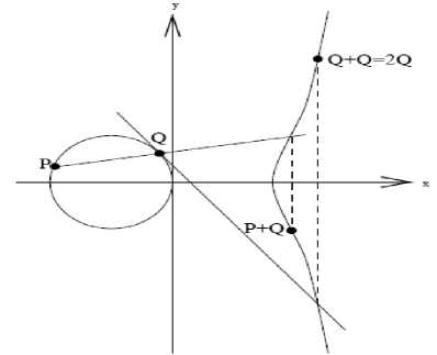
Each value of the ‘α’ and ‘β’ gives a different EC. All points (x, y) which satisfies the above equation plus a point at infinity lies on the elliptic curve. The public key is a point in the curve while the private key is a random number. The public key is generated by multiplying the private key with the generator point G in the curve. The generator point G, the curve parameters ‘α’ and ‘β’, together with few more constants constitutes the domain parameters of ECC. The fundamental operations on the ECC are point adding, doubling and scalar multiplication. A simple elliptic curve is shown in Fig.1.
-
Figure 1: A simple elliptic curve
Hence, the pair (x, y), x, y € GF (p), will be a point on the curve when (x, y) satisfies (1), and the point at infinity, denoted by ∞, is said to be on the curve. The algebraic formulae for point addition and point doubling are given as
X3=λ2–x1-x2(mod p)(2)
Y 3 = λ(x 1 -x 3 )-y 1 (mod p)
When P ≠ Q, λ= (y2–y1)/(x2–x1)(3)
When P=Q, λ= (3x12+α)/2y1(4)
The common arithmetic operations over GF (p) are the addition, subtraction, multiplication and inverse. In the EC operations, there are two type of coordinates, one is affine coordinate another is projective coordinate. One of the complex and time consuming operations on EC is field inversion. The affine coordinate contains the field inversion operation, while the alternative Jacobian’s projective coordinate is in the form (x,y,z) → (x/z2,y/z2) over GF (p).
The steps taken by two individuals in order to communicate a secret through an unsecured channel using ECC is significant. In this protocol both parts perform the same computation apart from the signal of the point multiplication. To encrypt the message M, C=M+k1 (k2G) is computed and to decrypt M=C-k 2 (k 1 G) is computed, with ‘ki’ the private keys and ‘kiG’ the public keys of the two individuals.
Performance Enhanced Co-Processor for Elliptic Curve Cryptography over GF (p)
An EC over GF (p) consists of the solutions (x,y) as defined by (1) along with an additional element called the point at infinity, denoted by Q. The set of points (x,y) are in the so-called affine coordinate representation. The operation of Q=kP is called point multiplication or scalar multiplication, where ‘k’ is an integer and ‘P’ is a point on an EC ‘E’ defined over a field GF(p), which dominates the execution time of ECC schemes. In the implementation of ECC, scalar multiplication and inversion are not only the basic computing but also the most time consuming operations. So the operational efficiency of inversion and scalar multiplication directly determines the performance of ECC.
Many ECC algorithm have been implemented [3],[9], and there were flexible and high speed either over GF(2m) or GF(p).The high speed parallel architecture have been implemented [3],[5] over GF(2m). In [6], high throughput and low power signs have been implemented over GF (p). The dual – field designs were proposed [7],[9], which are flexible, high throughput, parallel, and scalable for elliptic curve over GF (p) and GF (2m).
The proposed ECC processor has been synthesized using Xilinix ISE. Simulation was done with Modelsim XE 6.1e, and fabricated using TSMC 130-nm CMOS cell base technology. This coprocessor can be adapted both prime field and binary field, also contains a control unit with 256 bit serial and parallel operations , which provide integrated high throughput with low power consumptions. This test coprocessor can operate in the parallel mode with four arithmetic units (AUs) and serial mode with the single AU. This scalar Multiplier architecture operation is perform base on clock rate and produce better performance in term of time and area compared to similar works.
2. MATHEMATICAL BACKGROUND
In this work, we focus on ECC over binary field GF (2m) with polynomial basis defined in the IEEE 1363 Standard Specifications for Public-Key Cryptography [9]. The standardized Elliptic Curve (EC) is y2 +xy = x3 + ax2 + b, where a, b € GF (2m) and b _= 0. The most critical operation in ECC, i.e., the point scalar multiplication, can be defined as Q = kP, where Q and P are points on the EC and k is a scalar. The operation KP can be performed by iterative point double and point addition. Our ECC architecture adopts the Montgomery scalar multiplication with projective coordinate presented in [10] for fast point scalar multiplication as shown in algorithm 1.
Algorithm 2.1 Montgomery scalar multiplication with projective coordinate representation.
Input: A point P = ( x, y ), an l -bit integer k = ( kl- 1 , . . . , k 1 , k 0).
Output: Q = kP .
-
1: X 1 = x , Z 1 = 1, X 2 = x 4 +β, Z 2 = x 2.
-
2: for i = l- 2 to 0 by - 1 do
-
3: if ki = 1 then
-
4: ( X 1 ,Z 1 ) = M add ( X 1, Z 1, X 2, Z 2 ), ( X 2,, Z 2 ) = M double ( X 2, Z 2 )
-
5: else
-
6: ( X 2, Z 2 ) = M add ( X 1, Z 1, X 2, Z 2 ), ( X 1 ,Z 1) = M double ( X 1 ,Z 1 )
-
7: end if
-
8: end for
-
9: Q = M xy ( X 1, Z 1, X 2, Z 2 )
-
10:
-
11: M add ( X 1, Z 1, X 2, Z 2 ) // Point Addition
-
12: Z 3 = ( X 1 ×Z 2 + X 2 ×Z 1)2, X 3
= x×Z 3 +( X 1 ×Z 2) × ( X 2 ×Z 1)
-
13: return( X 3 ,Z 3)
-
14: Mdouble ( X 1 ,Z 1) // Point Double
-
15: Z 2 = Z 2 1 ×X 2
-
1, X 2 = X 4
-
1 + b×Z 4 1
16: return(X2,Z2)
17: Mxy(X1,Z1,X2,Z2) // Coordinate Conversion
18: X = X1/Z1, Y = (x+X)×(y+x2 +(X2/Z2 +x)×(X1/Z1 +x))/x+y
3. PROPOSED ECC ARCHITECTURE
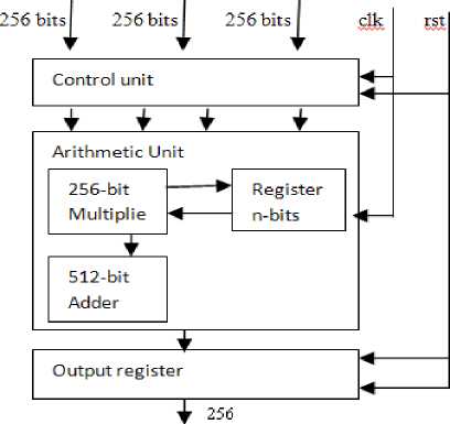
Fig.2, shows the proposed ECC scalar multiplication Architecture, which contains control units , dual field 256 bit multiplier and adder, and output register .The control unit decoded the four 256 bit instructions and send to the Arithmetic unit, which is performing the adding and doubling operations. In the dual field co-processor based on [6] and performs the Montgomery scalar multiplication over GF (2m) and Montgomery inversion over GF (p) we used Spartan II device to build up the processor. The EC point scalar multiplication can be done by iteratively point double and/or point double with point additions. This approach shows the significant improvements over [9], in term of performance and power efficiency. To speed up the performance, the coprocessor adopted full word field adder and it reduces 85% of the cycle for multiplicative inversion over finite field. To reduce the power consumption, it provides both the parallel and serial power modes.
bits
Figure 2. The ECC Modular Multiplier
Fig. 3 shows the proposed processor, which contains advanced high performance bus (AHB) interface, input and output buffers, Main controller, EC data selector, ECC modular multiplier, Clock controller, Register File, and Montgomery Unit. The EC Data selector fetches the instructions from the main controller and decoded to ECC Modular Multiplication units... The Clock Control Unit used for schedule the cycle required to perform the scalar multiplications. The ECC Modular Multiplier performs point coordinate conversion, point double, point addition, scalar multiplication, Montgomery pre and post processing, and modular exponentiation.
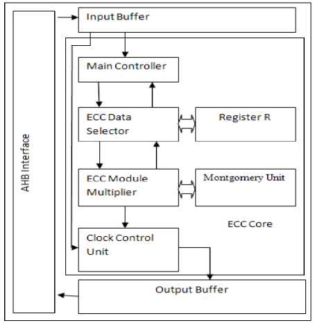
Figure 3. Block diagram of the ECC Processor chip
The Montgomery unit contains Montgomery Scheduler and Montgomery Data selector. The Montgomery Scheduler decodes instruction from the Phase II of Algorithm 2.1 and performs the Montgomery inversion. The Data Selector fetches the input value from the input buffer, the input values are either prime or binary field based on the curve over GF (p) and GF (2m), respectively. Our processor contains the dual – field adders which consist of four parallel units and one serial unit.
The main features of our design is , we used Altera Stratix II device and TMSC 0.13μm CMOS technologies are together in order to produce the low power and less area. The 256 bit ECC Modular Multiplier is embedding in between ECC Data Selector and Clock Control unit, which is produce better result compare with [14].
These four parallel and serial units are used to reduce the power consumptions. The four parallel Arithmetic Units and one serial unit are decodes control instructions from the main controller and perform the modular addition and modular multiplication, the intermediate results are stores in the register file. The dual-field multipliers and dual-field adders are capable of performing arithmetic over both the prime and binary fields by a unified hardware. Each intermediate variable during the EC operation is stored in the register file, which consists of seven 256-bit buffers. Finally, the output buffer stores the results, which can be accessed via the bus.
4. PERFORMANCE COMPARISION
The proposed design has been captured in Verilog HDL, simulated by ModelSim and implemented on Spartan II device. The FPGA design presented is highly adaptable and easily reprogrammable for both prime field and finite field and our design also fabricated by using TSMC 130 nm 1.6 V 1P8M CMOS standard.
Since the design used both Spartan II device and TSMC 130-nm CMOS cell-base technology, the comparison table contains previous works with both technologies. The Table II shows the comparison result of our design and previous similar works with different application specific integrated circuit (ASIC) design for both GF (p) and GF (2m), as most of them reported synthesis or post layout results
TABLE 2 PERFORMANCE COMPARISION OF OTHER DESIGNS
|
Design |
Device |
Implementation of Modular Multiplication |
Clock Cycles for One Operation |
Time for Operati on |
|
[6] |
0.13 ASIC |
Systolic array |
120 Cycles |
1.2 µs |
|
100 MHz |
||||
|
[7] |
Xilinx Virtex- E V1000 E |
Systolic array |
230 Cycles |
2.6 µs |
|
91.3 MHz |
||||
|
[8] |
Xilinx Virtex2 pro XC2VI P125 |
256 embedded multipliers used |
32 Cycles |
0.7 µs |
|
45.68 MHz |
||||
|
[9] |
0.18 ASIC |
Custom-designed 256-bit multiplier |
3 Cycles |
0.021 µs |
|
142 MHz |
||||
|
Ours |
Altera Cyclon e3 EP3C4 0 |
81 embedded multipliers used |
3 Cycles |
0.1 µs |
|
130.38 Hz |
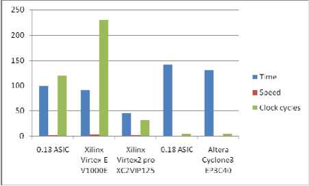
Fig.4 Performance Comparison
5. CONCLUSION
In this work, a new 256-bit Montgomery multiplier has been designed. With the 5-stage pipeline, it can perform a modular multiplication in only 3 cycles. To our knowledge, it is much faster than previous designs on FPGA devices. By using Karatusba-Ofman algorithm, the number of embedded multipliers required is reduced on FPGA devices. Furthermore, the design can be easily merged by some other IPs to build a full cryptographic SOC system.
References Hardware Implementation of Elliptic Curve Cryptography over Binary Field
- Certicom Corporation, The Basics of ECC 2006[Online] available: http://www.certicom.com/indexphp? Action=res, ecc_fa
- IEEE 1363 standard specifications for public-key cryptography, 1363, Jan. 2000
- B. Ansari and M. A. Hasan, “High-performance architecture of elliptic curve scalar multiplication” IEEE Trans. Computers, vol. 57, no. 11,pp. 1143–1153, Nov. 2008.
- K. Jarvinen and J. Skytta, “On parallelization of high-speed processors for elliptic curve cryptography” IEEE Trans. Very Large Scale Integer. (VLSI) Syst., vol. 16, no. 9, pp. 1162–1175, Sep. 2008.
- Z.-B. Dai, F. Qin, and X.-H. Yang, “Scalable hardware architecture for Montgomery inversion computation in dual-field” in Proc. WASE Int.Conf. Inf. Eng., Taiyuan, China, Jul. 2009, pp. 206–209.
- Yaxun Gong, Shuguo Li,”High-Throughput FPGA Implementation of 256-bit Montgomery Modular Multiplier” in Proc IEEE on Second International Workshop on Education Technology and Computer Science, (ETCS), Jan 2010,pp.173-177.
- G. Chen, G. Bai, and H. Chen, “A dual-field elliptic curve cryptographic processor based on a systolic arithmetic unit” in Proc. IEEE Int. Symp.Circuits Syst. (ISCAS), Seattle, WA, May 2008, pp. 3298–3301.
- J.-Y. Lai and C.-T. Huang, “Elixir: High-throughput cost-effective dualfieldProcessors and the design framework for elliptic curve cryptography” IEEE Trans. Very Large Scale Integer. (VLSI) Syst., vol. 16, no. 11, pp. 1567–1580, Nov. 2008.
- J.-Y. Lai and C.-T. Huang, “A highly efficient cipher processor for dual field elliptic curve cryptography” IEEE Trans. Circuits Syst. II, Expr. Briefs, vol. 56, no. 5, pp. 394–398, May 2009.
- J. Lopez and R. Dahab, “Improved algorithms for elliptic curve arithmetic in GF (2m)” in Proc. Sel. Areas Cryptography: 5th Annu. Int. Workshop (SAC), Aug. 1998, vol. 1556, pp. 201–212.
- C.J.McIvor, M.McLoone, and J.V.McCanny,”Hardware Elliptic Curve Cryptographic Processor over GF (P)” IEEE Transacitons on circuits and systems-I: Regular Papers. VOL.53.No.9, September 2006
- B. S. Kaliski Jr., “The Montgomery inverse and its applications” IEEE Trans. Computers, vol. 44, no. 8, pp. 1064–1065, Aug. 1995.
- E. Savas,, M. Naseer, A. A. A. Gutub, and C. K. Koc, “Efficient unified Montgomery inversion with multibit shifting” IEEE Proc. — Comput.Digit. Techn. vol. 152, no. 4, pp. 489–498, Jul. 2005.
- J.-Y. Lai and C.-T. Huang, “Energy-Adaptive Dual-Field Processor for High-Performance Elliptic Curve Cryptographic Applications” IEEE Trans. Onvery large scale integration (VLSI) systems.vol 56, no. 4, pp.356-360, March 2010.
- J. Goodman and A. P. Chandrakasan, “An energy-efficient reconfigurable public-key cryptography processor” IEEE J. Solid-StateCircuits, vol. 36, no. 11, pp. 1808–1820, Nov. 2001.
