High Performance FPGA Based Digital Space Vector PWM Three Phase Voltage Source Inverter

Author: Bahram Rashidi, Mehran Sabahi
Journal: International Journal of Modern Education and Computer Science (IJMECS) @ijmecs
Article in issue: 1 vol.5, 2013.
Free access
This paper focuses on the design of a low power and high performance FPGA based Digital Space Vector Pulse Width Modulation (DSVPWM) controller for three phase voltage source inverter. A new method is proposed to realize easy, accurate and high performance DSVPWM technique based on FPGA with low resource consumption and reduced execution time than conventional methods. Equations of SVPWM are relatively complicated and need a considerable time to execute on a typical microcontroller, therefore a simple method is presented to minimize run time of instructions, e.g. the multiplication operation used in these equations is replaced by a proposed signed and unsigned shifter using 2 to 1 multiplexer unit. Total power consumption of controller is reduced to 37 mW at 100MHz clock frequency. The proposed DSVPWM technique algorithm was synthesized and implemented using Quartus II 9.1V and Cyclone II FPGA, to target device EP2C20F484C6. Also power is analyzed using XPower analyzer. Experimentation and results demonstrate that proposed method have high performance than other works.
DSVPWM, Voltage Source Inverter, FPGA, VHDL, Combinational Logic
Short address: https://sciup.org/15014515
IDR: 15014515
Text of the scientific article High Performance FPGA Based Digital Space Vector PWM Three Phase Voltage Source Inverter
The SVPWM technique offers significant performance benefits and has proved to be very popular in three-phase systems [1-4]. Pulse Width Modulation variable speed drives are increasingly applied in many new industrial applications that require superior performance. Recently, developments in power electronics and semiconductor technology have lead improvements in power electronic systems. Hence, different circuit configurations namely multilevel inverters have become popular and considerable interest by researcher are given on them. Variable voltage and frequency supply to ac drives is invariably obtained from a three-phase voltage source inverter. A number of Pulse width modulation (PWM) schemes are used to obtain variable voltage and frequency supply. The most widely used PWM schemes for three-phase voltage source inverters are carrier-based sinusoidal PWM and space vector PWM (SVPWM). There is an increasing trend of using Space Vector PWM (SVPWM) because of their easier digital realization and better dc bus utilization. As seen from the above discussion Space Vector PWM is superior as compared to Sinusoidal pulse width modulation in many aspects like:
-
1- The Modulation Index is higher for SVPWM as compared to SPWM.
-
2- The output voltage is about 15% more in case of SVPWM as compared to SPWM.
-
3- The current and torque harmonics produced are much less in case of SVPWM.
However despite all the above mentioned advantages that SVPWM enjoy over SPWM, SVPWM algorithm used in three-level inverters is more complex because of large number of inverter switching states. Hence we see that there is a certain trade off that exists while using SVPWM for inverters for Adjustable speed Drive Operations. Due to this we have to choose carefully as to which of the two techniques to use weighing the pros and cons of each method [2]. Recently some control systems have been considered to deign using field-programmable gate array, FPGA integrated circuit. Implementation of SVPWM by using FPGA has been studied by a few researchers; a novel space vector pulse width modulation (SVPWM) algorithm for multilevel multiphase voltage source converters is presented in [1]. In [3], a resource efficient SVPWM algorithm is proposed which reduces computational overheads and solves the problem of high sampling time in real time applications. In [4], a simple realization of 5-segment discontinuous SVPWM, with simple calculation of the firing has been presented.
This paper focuses on the design of a low power and high performance FPGA based Digital Space Vector Pulse Width Modulation (DSVPWM) controller for three phase voltage source inverter.
-
II. the proposed high performance dsvpwm signal
GENERATION STRATEGY
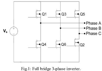
A 3-phase output can be obtained from a configuration of six transistors as shown in Fig. 1. The concept of SVPWM has been fully studied in several lectures therefore the required equations are available. The proposed method used in this design, is to replace the conventional method with the hardware description language VHDL on FPGA, based on high performance digital circuit, which better accuracy and performance are obtained by field generated pulses of PWM. The use of the FPGA brings flexibility to change the real-time control algorithms without further changes in hardware. It will reduce the overall cost and has a small size of control circuit for the three phase full bridge inverter. The aim of this research is mainly to design and develop the SPWM switching method to FPGA based DSVPWM on three phase voltage source inverter. Proposed design is based on optimized digital circuit.
-
A. Principle of Space Vector PWM
The sinusoidal voltage treats as a constant amplitude vector rotating at constant frequency. This PWM technique approximates the reference voltage V ref by a combination of the eight switching patterns (V 0 to V 7 ). Coordinate Transformation (abc reference frame to the stationary d-q frame): A three-phase voltage vector is transformed into a vector in the stationary d-q coordinate frame which represents the spatial vector sum of the three-phase voltage. The vectors (V 1 to V 6 ) divide the plane into six sectors (each sector: 60 degrees). V ref is generated by two adjacent non zero vectors and two zero vectors. Basic switching vectors and Sectors [7]:
6 active vectors (V 1 , V2, V 3 , V 4 , V 5 , V 6 )
Axes of a hexagonal
DC link voltage is supplied to the load
Each sector (1 to 6): 60 degrees
Basic switching vectors and Sectors are shows in Fig.2.
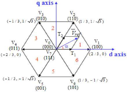
Fig.2: Basic switching vectors and sectors.
-
B. Realization of Space Vector PWM:
-
• Step 1. Determine V d , V q , Vref, and angle ( a )
-
• Step 2. Determine time duration T1, T2, T0
• Step 3. Determine the switching time of each transistor (S 1 to S 6 )
Step 1: Determine V d , V q , Vre f and angle (a)
To implement the space vector PWM, the voltage equations in the abc reference frame can be transformed into the stationary d-q reference frame that consists of the horizontal (d) and vertical (q) axis as depicted in Fig.3.
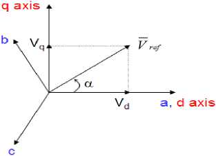
Fig.3: Voltage Space Vector and its components in (d, q).
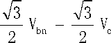
The relationship between switching variable vector and phase voltage vector [V a V b V c ] can be expressed as follows [3]:
Vd = Van - Vbn • cos60 - Vcn • cos60
V an
- 2 V bn
1V
2 cn
V = 0 + Vbn • cos30 - Vcn • cos30
q n cn
V d
V q
—
Van
Vbn
V cn
The reference vector V ref is calculated as [3]:
1 V ref = J V d2 + Vq2
V a = tan 1 ( -) = w t = 2пд, t
Vd s s
(Where, f s = fundamental frequency)
In general, V ref in ‘n’ sector is obtained by two adjacent non-zero vectors (V n , V n+1 ) and two-zero vectors. V ref is expressed as [3]:
V f = T n- V + T n + 1 V , (3'
ref . n n + 1
T Z T Z
Where T n & T n+1 are on time of V n and V n+1 during each sampling period (T z ) respectively and ‘n’ is the sector number in which V ref resides.
Step 2: Determine Time Duration T 1 , T 2 , T 0
The switching time duration T 1 , T 2 and T 0 for a particular sector can be calculated from following equations [3].
Fig. 4 shows reference vector as a combination of adjacent vectors at sector 1.
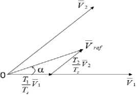
Fig. 4: Reference vector as a combination of adjacent vectors at sector
Step 3. Determine The Switching Time Of Each
Transistor (S 1 To S 6 )
Switching time duration at Sector 1:
T z T , T , + T2 T z
J V ref = J V 1 dt + J V 2 dt + J V o
0 0 T1 T1 + T 2
л T z ■ V ref = (T 1 ■ V 1 + T2 - V 2 )
^ T z ■ I V ref I
cos( α ) sin ( α )
= T - 2 ■ V
+
л T = Tz - a -
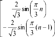
л T = T - a -
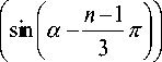
sin ( n /3 - a ) sin ( n /3) sin ( a )
sin ( n /3)
• T o = T z - ( T 1 + T 2 ),
where, T = — and , z fs
\
Switching time duration at any Sector
• T =
• T
• • T 2
n
n - 1
Vdc
dc
dc
sin I - a + n
n sin n cos a -
V3 ■ T ■ ^геД ------------------------L
Vdc
V3 ■ T\Vref\
• T - T-T-T
•• T o T z T 1 T 2 ,
T ■ 2 ■ V ■
2 3 dc
cos( π /3) sin ( π /3)
(where, 0≤α≤60°)
a = Ы 2V d.
3 7
n cos n sin a
. n -1 . n -1
- cos a ■ sin n + sin a ■ cos
n = 1 through 6 ( that is, Sector 1 to 6) 0 < a < 60 °
The switching time of each switching devices (S 1 ~S 6 ) per sector is given as per Table I
TABLE I: SWITCHING TIME AT EACH SECTOR.
|
Sector |
S 1 , S 3 , S 5 |
S 2 , S 4 , S 6 |
|
1 |
S 1 = T 1 + T 2 + T 0 /2 S 3 = T 2 + T 0 /2 S 5 = T 0 /2 |
S 4 = T 0 /2 S 6 = T 1 + T 0 /2 S 2 = T 1 + T 2 + T 0 /2 |
|
2 |
S 1 = T 1 + T 0 /2 S 3 = T 1 +T 2 + T 0 /2 S 5 = T 0 /2 |
S 4 = T 2 +T 0 /2 S 6 = T 0 /2 S 2 = T 1 +T 2 +T 0 /2 |
|
3 |
S1= T0/2 S3= T1+T2+T0/2 S5= T1+T2 |
S 4 = T 1 +T 2 +T 0 /2 S 6 = T 0 /2 S 2 = T 1 +T 0 /2 |
|
4 |
S 1 = T 0 /2 S 3 = T 1 +T 0 /2 S 5 = T 1 +T 2 +T 0 /2 |
S 4 = T 1 +T 2 +T 0 /2 S 6 = T 2 +T 0 /2 S 2 = T 0 /2 |
|
5 |
S 1 = T 2 +T 0 /2 S 3 = T 0 /2 S 5 = T 1 +T 2 +T 0 /2 |
S 4 = T 1 +T 0 /2 S 6 = T 1 +T 2 +T 0 /2 S 2 = T 0 /2 |
|
6 |
S 1 = T 1 +T 2 +T 0 /2 S 3 = T 0 /2 S 5 = T 1 +T 0 /2 |
S 4 = T 0 /2 S 6 = T 1 +T 2 +T 0 /2 S 2 = T 2 +T 0 /2 |
The sector identification criterion of conventional algorithm involves floating point operations as to get angle that requires calculating inverse tan function.
Because of sine function and square root values involved in computation switching time duration i.e. T 1 , T 2 and T 0 , implementation of conventional algorithm using digital processor becomes difficult [3].
-
C. Proposed Implementation of DSVPWM on FPGA
Today digital designers use hardware description languages (HDLs) to design digital systems. The most widely used HDLs are VHDL and Verilog. Both of these hardware description languages allow the user to design digital systems by writing a program that describes the behavior of the digital circuit. The program can then be used to both simulate the operation of the circuit and synthesize an actual implementation of the circuit in a CPLD, an FPGA, or an application specific integrated circuit (ASIC). Another recent trend is to design digital circuits using block diagrams or graphic symbols that represent higher-level design constructs. These block diagrams can then be compiled to produce Verilog or VHDL code. VHDL is based on the Ada software programming language but it is not Ada nor is it a software programming language. VHDL is a hardware description language that is designed to model digital logic circuits. It simply has syntax similar to the Ada programming language but the way it behaves is different [8]. In this paper we use of hardware description language VHDL for design and implement full-DSVPWM based on combinational logic circuits with low resource utilization and reduces execution time. We use simplify mathematical equations which require only addition, subtraction, shifting (combinational based on proposed signed shifter). We implement the DSVPWM algorithm for three phase voltage source inverter on an Induction Motor based on FPGA. in continue we decryption proposed method.
-
D. Computation X d and X q based on V a , V b and V c with proposed signed shifter
The conventional SVPWM algorithm includes d-q transformation of three input voltages V an , V bn and V cn as given by equation (4) this transformation requires value of 3 to be calculated it is difficult to implement floating point numbers using FPGA. Hence instead of d-q transformation, intermediate transformation vectors are used. The eq. (1) can be written as [3]:
V. = 2V - 1V - 1V d3a3b3c
V = -1V q V3 b

- Vd = 1[2V. - Vb - Vc]
Vq = ^[Vb - Vc]
By defining intermediate variables as Xd and Xq, the eq. (7) written as [3]:
Xd = 2Va - Vb - V
Xq = Vb - V
In continue we present proposed circuit and digital design for implementation of X d and X q based on eq.(9) thus we for this work implement 2V a alone with shift operation without use multiplier and two subtractor. For implementation of 2V a proposed combinational signed shifter based on (2 to 1) multiplexer, Shifter block is made only based on multiplexer. The input is an 8-bit vector, the output is a shifted version of the input, it shift input to left from 0 to 7(if number is 8 bits) proportional to the weight of select bits (sel[2..0]). If the value of select bits is 0, we have non-shift otherwise we have shift proportional to the weight of select bits. The circuit consists of three individual barrel shifters. Notice that the first barrel has only one ‘0’connected to one of the multiplexers while the second has two, and the third has four. For larger vectors, we would just keep doubling the number of ‘0’ inputs. If shift ‘‘001’’, for example, then only the first barrel should cause a shift; on the other hand, if shift ‘‘111’’, then all barrels should cause a shift. Thus for compute 2V a we select S1_0=’1’, S1_1=’0’, S1_2=’0’. Fig. 5 shows an unsigned shifter block.
Va[7]
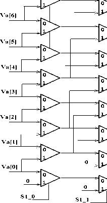
O[6]
O[5]
O[4]
O[3]
O[2]
O[1]
O[0]
Fig.5: Unsigned shifter block.
O[7]
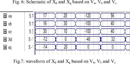
Hence the proposed method to calculate X d and X q needs only simple operators namely shifter (for 2V a i.e. multiplication by 2), and subtractor that all are combinational circuits without clock signal and extra hardware proposed implementation of this block is completely optimized and low power because this block is only based on 2 to 1 multiplexer. Fig. 6 and Fig. 7 shows schematic and waveform of proposed VHDL code for compute X d and X q based on V a , V b and V c .
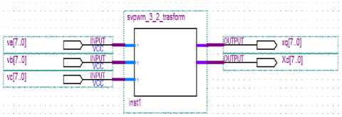
|
va[7..O] |
|
|
xd[7..O] |
|
|
vc[7..O] |
By combining eq. (8) and (9), the V d and V q are expressed in terms of intermediate vectors as [3]:
A Vd = 1[Xd]
V=^[Xq]
-
E. Determination of The Sectors With Proposed Digital Design
The determination of sector depends only on the sign of X d and X q as per following rules. Determination of the sectors can be done by simply checking 3 conditions:
Condition 1: sign of X d
Condition 2: sign of X q
Condition 3: |X d | > |X q /2|
We do this part with a simple combination logic circuits have been implemented. First implement condition 1 and then condition 2 is implemented in continue we implement Expression Xq/2 with Shift to the right one bit. Than |X d |, |X q /2| with proposed digital circuit implemented without use of abs () function. Total of three condition 1, condition 2 and condition 3 are design and implementation with optimized and combinational logic circuit.
The rules to find sectors base on [3]:
Rule 1: if (X d >0 & X q >0 & |X d |>|X q /2|) Sector-1
Rule 2: if (X d >0 & X q >0 & |X d |<|X q /2|) Sector-2 OR if (X d <0 & X q >0 & |X d |<|X q /2|) Sector-2
Rule 3: if (X d <0 & X q >0 & |X d |>|X q /2|) Sector-3
Rule 4: if (X d <0 & X q <0 & |X d |>|X q /2|) Sector-4
Rule 5: if (X d >0 & X q <0 & |X d |<|X q /2|) Sector-5 OR if (X d <0 & X q <0 & |X d |<|X q /2|) Sector-5
Rule 6: if (X d >0 & X q <0 & |X d |>|X q /2|) Sector-6
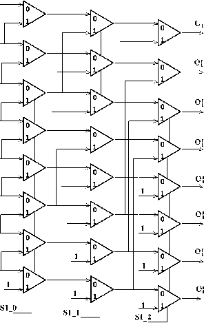
Proposed digital design for sector determination is shows in Fig. 8 as see we implement Rule 1 to Rule 6 based on simple and low power logic circuits proposed design is based on combinational logic circuits thus we increase performance and reduced power consumption. This proposed digital circuit implement sector determination completely and accurate. For increase performance of design can use sub-pipelining technique.
Fig. 8: Proposed digital design for sector determination.
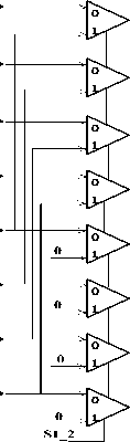
Xq[0]
O[0]
Xq[1]
Xq[2]
Xq[5]
O[1]
O[2]
O[3]
O[4]
O[5]
O[6]
O[7]
(a)
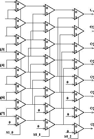
Fig.9: (a) Proposed signed shifter B, (b) Proposed signed shifter A.
Xq[0]
O[0]
Xq[1]
Xq[2]
Xq[3]
Xq[5]
Xq[6]
Xq[7]
O[1]
O[2]
O[3]
O[4]
O[5]
O[6]
O[7]
(b)
For compute X q /2 use signed shift to right one bit thus we make a signed shifter in this signed shifter, ordering of input number be inverse indeed X q [7..0] replace with X q [0..7] that must enter to proposed signed shifter. Signed shifter A and B are based on combinational digital circuits with 2 to 1 multiplexer. Proposed signed shifter block is shown in Fig. 9.
Schematic and waveform of sector determination are shows in Fig. 10 and Fig. 11.
Eq. (11) shows that every PWM period, the output voltages are approximated as (T z /V dc ) by switching between the two none zero basic vectors that border the sector of the current output voltages. The sum of T n and T n+1 should be less than or equal to T PWM and rest of period the switching time should be T 0 The M 0 is called as decomposition matrix, given as applying equation (10) to (6), the switching time can be calculated as [3]:
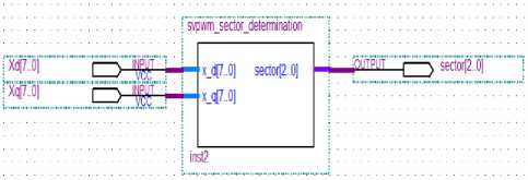
Fig.10: Schematic proposed method for implementation sector determination.
M 0
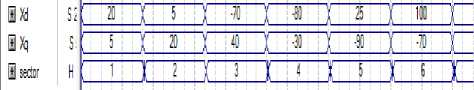
Fig. 11: Waveform proposed method for implementation sector determination.
F. Determination Switching Times With Proposed Digital Design
For a symmetric space vector PWM, the output voltage i.e. X d and X q can be in any of the sector 1 to sector 6 is given by the equation [3]:
T n
. Tn+1 J
= T PWM M 0
X d
X q
M 00 M 01
M 10 M 11

cosl — (n -1)
I 3
If vdc is normalized with 3 per unit, and Tz is set to 3 per unit, the four coefficients in eq. (12) will alter their values according to the sector ‘n’. If reference vector is located in sector I, then ‘n’=1, then M00=1, M01=-1/2, M10=0, M11=1. The coefficients of decomposition matrix according to sector are given in Table II [3].
TABLE II: COEFFICIENTS OF DECOMPOSITION MATRIX
|
Sector ‘n’ |
1 |
2 |
3 |
4 |
5 |
6 |
|
M 00 |
1 |
1 |
0 |
-1 |
-1 |
0 |
|
M 01 |
-1/2 |
1/2 |
1 |
1/2 |
-1/2 |
-1 |
|
M 10 |
0 |
-1 |
-1 |
0 |
1 |
1 |
|
M 11 |
1 |
1/2 |
-1/2 |
-1 |
-1/2 |
1/2 |
So form eq.(11) the switching times are calculated as:
T n
= [ M oo M oi ] vd
T
T n + 1
= [ M io M„ ]
T
T0
r- '
3 - T n + T,
X' X( 'n + 1 '
d
q _
Fig. 13 shows waveform of implementation x .
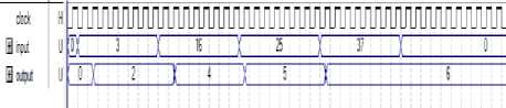
Fig. 13: Waveform of proposed method for implementation x
Proposed implementation algorithm for compute the switching times show in below
If(sector=1)=>T n =X d -shift_to_right(X q ),T n+1 =X q ,T 0 = 3 -T n +T n+1 If(sector=2)=>T n =X d +shift_to_right(X q ),T n+1 = shift_to_right(X q )-X d ,T 0 = 3 -T n +T n+1 If(sector=3)=>T n =X q ,T n+1 =-X d -shift_to_right(X q ),T 0 = 3 -T n +T n+1
If(sector=4)=>T n =-X d +shift_to_right(X q ),T n+1 =-X q ,T 0 = 3 -T n +T n+1
If(sector=5)=>T n =-X d -shift_to_right(X q ),T n+1 =X d -shift_to_right(X q ),T 0 = 3 -T n +T n+1
If(sector=6)=>T n =-X q ,
T n+1 =X d +shift_to_right(X q ),T 0 = 3 -T n +T n+1
In this part for implementation we use of Tn, Tn+1 and T0 use shift to the right, additional and subtraction operation without use multiplier. We for implement 3 use a new technique based on logic shift without any complexity. Logic shifter is based on unsigned combinational shifter show in figure 4 that is design only with 2 to 1 multiplexer schematic of operation proposed method for implement x thus beginning number 1 with unsigned shift block shifted one bit to left and then compare with input number if input number is bigger of shifted number counter one unit increase until shifted number being bigger input number in end counter number is load in output register. Schematic of proposed method is shown in Fig.12 if input equal 3 thus 3 is compute.
Input
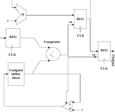
Fig.12: Schematic of proposed method for implementation x
Schematic and waveform of switching times are shows in Figure 14 and Figure 15.
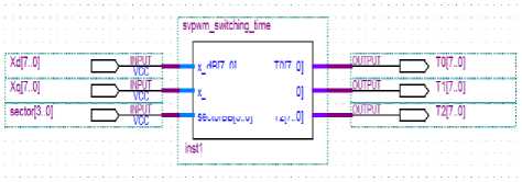
Fig. 14: Schematic proposed method for implementation switching times.
|
x_dBp..O] |
тор.,о] |
|
x_qBp..O] |
T1P..0] |
|
sectorBB[3..0] |
T2P..0] |
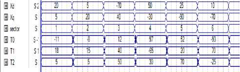
Fig.15: Waveform proposed method for implementation switching times.
-
G. Proposed SVPWM Pulses Generation Module
In following proposed PWM generation module is presented. Time duration of any PWM pulse is dependent number of sector and switching times T0, T1 and T2 in order to implementation of PWM generation use a counter. Range of counter is 1 to (T0/2 + T2 + T1 + T0/2 + T0/2 + T1 + T2 + T0/2 = 2*T0 + 2*T1 + 2*T2) now proportional number of sector and counter amount PWM pulse is ‘0’ or ‘1’.
For sector 1 and 2 range of counter is 1 to (2*T0 +
2*T1 + 2*T2):
If (Sector=1) => {
If (counter =T0/2) => PWM_A=’1’, PWM_B=’0’, PWM_C=’0’;
If (counter = T0/2+T1) => PWM_A=’1’, PWM_B=’1’, PWM_C=’0’;
If (counter = T0/2+T1+T2) => PWM_A=’1’,
PWM_B=’1’, PWM_C=’1’;
If (counter = T0+T1+T2) => PWM_A=’1’,
PWM_B=’1’, PWM_C=’1’;
If (counter = T0+T1+T2+T0/2) => PWM_A=’1’,
PWM_B=’1’, PWM_C=’0’;
If (counter = T0+T1+2T2+T0/2) => PWM_A=’1’,
PWM_B=’0’, PWM_C=’0’;
If (counter = T0+2T1+2T2+T0/2) => PWM_A=’0’, PWM_B=’0’, PWM_C=’0’;
If (counter =2T0+2T1+2T2) => PWM_A=’0’, PWM_B=’0’, PWM_C=’0’;
}
The proposed calculation for this block is implemented based on simple operators such as shifters, adders. Thus the proposed implementation reduces the complexity, power consumption and increase performance total of algorithm of conventional SVPWM implementation.
-
III. comparison and experimentation
In order to get actual numbers for the hardware usage, this work is synthesized and implemented by Quartus-II-9.1V software and cyclone-II FPGA to target device EP2C20F484C6, also power is analyzed using Xilinx XPower analyzer. SVPWM pulses are applied to a three phase VSI via an optical interface. A low power induction motor is used as output load of the inverter. Also a dc power supply is used to provide dc-link voltage. Fig.16 shows waveform of proposed PWM generation for sectors 5 and 6 Fig. 17 shows waveform of proposed PWM generation for sectors1 and 2.
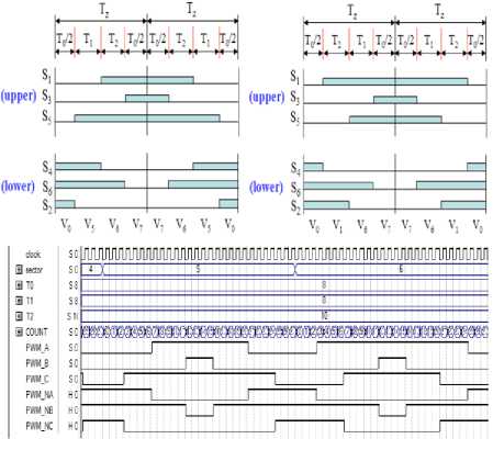
Fig.16: Waveform of proposed PWM generation for sectors 5 and 6.
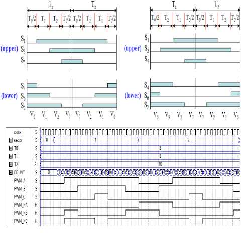
Fig.17: Waveform of proposed PWM generation for sectors 1 and 2.
Fig.18 shows waveform of proposed PWM generation for sectors 3 and 4.
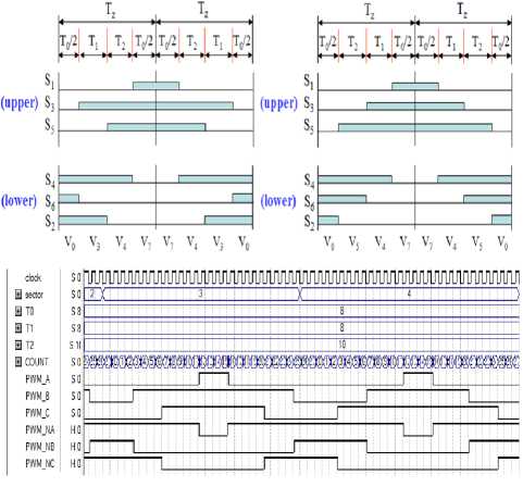
Fig.18: Waveform of proposed PWM generation for sectors 3 and 4.
Fig. 19 shows total block diagram of proposed DSVPWM on FPGA. Pipelining techniques between blocks and also sub-pipelining techniques in any blocks can be used to increase the total performance design for future works.
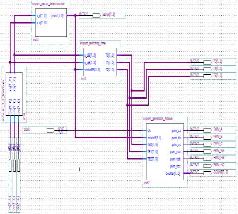
Fig. 19: Total block diagram of proposed DSVPWM on FPGA.
Waveform of proposed DSVPWM on FPGA is shows in Fig. 20.
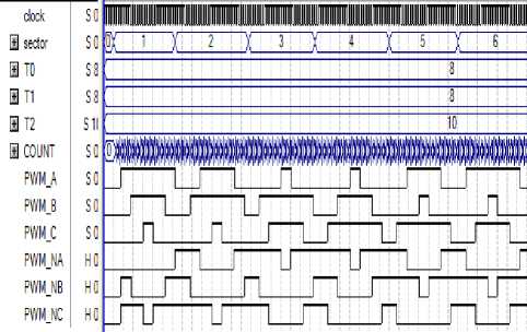
Fig.20: Waveform of proposed DSVPWM on FPGA.
The Fig.21 shows starter board cyclone II to target device EP2C20F484C6 and Fig.22 shows figures of actual hardware and experimentation for proposed method.
VII shows utilized hardware on FPGA and the type of device that has been used in [4][3][9].
TABLE III: UTILIZED HARDWARE ON FPGA IN PROPOSED METHOD
|
Implementati on |
Total logic elements |
Total combination al functions |
Total registers |
Frequenc y(Mhz) |
|
Proposed method |
392(2%) |
388(2%) |
88(1%) |
253.852 |
TABLE IV: SUMMARY OF DATA OBTAINED FROM POWER CONSUMPTION OF PROPOSED METHOD WITH XPOWER
|
Clock Frequncy(MHz) |
Dynamic power consumption(mW) |
|
100 |
37 |
|
75 |
33 |
|
50 |
28 |
|
25 |
23 |
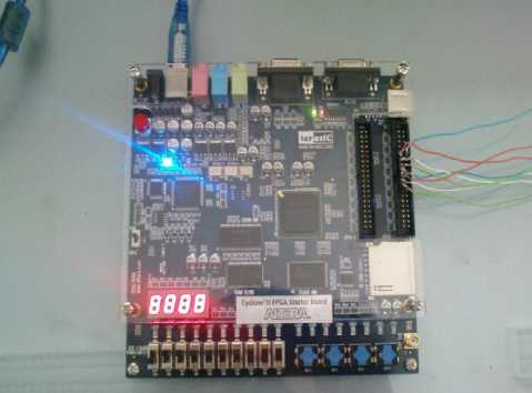
Fig. 21: Starter board cyclone II to target device EP2C20F484C6.
TABLE V: UTILIZED HARDWARE ON FPGA IN [4]
|
Implementati on |
Device |
Total of logic elements |
Total memory bits |
LC Register s |
|
[4] |
EP20k200E FC484-2X |
520(6%) |
9216(9%) |
31 |
TABLE VI: UTILIZED HARDWARE ON FPGA IN [3]
|
Implement ation |
Multipliers |
Dividers |
Adders/s ubtractor s |
CLB s |
Utilizat ion |
|
[3] |
0 |
0 |
32 |
490 |
4% |
TABLE VII: UTILIZED HARDWARE ON FPGA IN [9]
|
Implementatio n |
Device |
Numbe r of CLBs |
Numbe r of flipflops |
Max RAM bits |
Numb er of IOBs |
|
[9] |
Xc4003 A |
100 |
360 |
3200 |
80 |
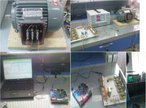
Fig. 22: Figures of actual hardware and experimentation for proposed method.
Table III shows the comparison between utilized hardware on FPGA and the type of device that has been used in proposed method, also Table IV shows Summary of data obtained from power consumption of our proposed method with Xpower and Tables V, VI,
-
IV. conclusion
In this paper a novel FPGA based digital space vector pulse width (DSVPWM) for three phase voltage source inverter has been designed using VHDL hardware description language. The advantages of this technique over the other literatures include flexibility, high accuracy and reduced area. Therefore a simple method has been presented to change complicate SVPWM equations to collection of shift, add and other similar uncomplicated orders to minimize run time of instructions. Proposed method has high performance, Stress Reduction, low power and high accuracy. To verify the proposed design a laboratory prototype has been arranged using of cyclone II FPGA board, an optical interface as IGBT drivers of voltage source inverter with an induction motor output load. Laboratory experiments and Xpower analyzer results demonstrate that, because of reduced hardware usage percentage, easy and fast instructions, proposed method has better performance and less power consumption than others works.
References High Performance FPGA Based Digital Space Vector PWM Three Phase Voltage Source Inverter
- Óscar López, Jacobo Álvarez, Jesús Doval-Gandoy, and Francisco D. Freijedo, "Multilevel Multiphase Space Vector PWM Algorithm", IEEE TRANSACTIONS ON INDUSTRIAL ELECTRONICS, VOL. 55, NO. 5, pp. 1933-1942, MAY 2008.
- Sunil Panda, Anupam Mishra, B. Srinivas, "Control of Voltage Source Inverters using PWM/SVPWM for Adjustable Speed Drive Applications", the award of the degree of BACHELOR OF TECHNOLOGY in ELECTRICAL ENGINEERING, Department of Electrical Engineering National Institute Of Technology Rourkela, May 2009.
- D. N. Sonawane, M. S. Sutaone , B. N. Choudhari and Abhijeet Badurkar, "FPGA Implementation of Simplified SVPWM Algorithm for Three Phase Voltage Source Inverter", International Journal of Computer and Electrical Engineering, Vol.2, No.6, pp. 1010-1017, December, 2010.
- Tole Sutikno, Member, IEEE, Auzani Jidin, Member, IEEE and Mohd Farriz Basar, Member, IEEE, "Simple Realization of 5-Segment Discontinuous SVPWM Based on FPGA", International Journal of Computer and Electrical Engineering, Vol. 2, No. 1, pp. 147-157, February, 2010.
- N. M. Nayan, "Design of a Microcontroller-Based Converter for 3-Phase Brushless DC Motor Drives", Thesis for Masters of Science, UNIVERSITI SAINS MALAYSIA, September 2009.
- BAHARUDDIN BIN ISMAIL, "DESIGN AND DEVELOPMENT OF UNIPOLAR SPWM SWITCHING PULSES FOR SINGLE PHASE FULL BRIDGE INVERTER APPLICATION", Thesis submitted in fulfilment of the requirements for the degree of Master of Science, May 2008.
- H.W. van der Broeck, H.-C. Skudelny, and G.V. Stanke, "Analysis and realization of a pulsewidth modulator based on voltage space vectors," IEEE Transactions on Industry Applications, vol.24, pp. 142-150, 1988.
- Richard E. Haskell, Darrin M. Hanna, "Introduction to Digital Design Using Digilent FPGA Boards", Published by LBE Books, LLC, 2009.
- Ying-Yu Tzou, Member, IEEE, and Hau-Jean Hsu, "FPGA Realization of Space-Vector PWM Control IC for Three-Phase PWM Inverters", IEEE TRANSACTIONS ON POWER ELECTRONICS, VOL. 12, NO. 6, pp. 953-963, NOVEMBER 1997.
