High-resolution X-ray imaging for industrial process monitoring and quality control

Author: Zschech E., Chukalina M.V., Bulatov K.B.
Journal: Компьютерная оптика @computer-optics
Section: International conference on machine vision
Article in issue: 6 т.49, 2025.
Free access
High-resolution X-ray imaging is an essential component of advanced workflows for industrial process monitoring and quality control (e.g., for metrology and defect inspection in the semiconductor industry). Depending on the specific application area, however, it is subject to different requirements, particularly regarding imaging accuracy and reconstruction fidelity, which are analyzed and systematically structured in this study. As an example, a seamless workflow of two nondestructive techniques with different spatial resolution and different throughput (here shown for a combination of acoustic and X-ray techniques) is proposed to auto-detect and auto-classify defects. X-ray microcopy and high-resolution X-ray computed tomography (XCT) provide nondestructive characterization capabilities on opaque objects, observing features with sizes down to several 10 nanometers. Because of the ability of micro-XCT and nano-XCT to reveal structural characteristics, to determine deviations from a well-defined standard, or to observe kinetic processes, they are suitable imaging techniques for micro- and nano-structured objects, but also for industrial process monitoring and quality control. Typical applications of high-resolution XCT are categorized into 3 groups: 1) Structure analysis – Creation of 3D digital images of the complete interior structure of an opaque object, 2) Flaw detection – Monitoring industrial processes and defect inspection, and 3) Quality control – Observing kinetic processes in objects important for industrial quality control and reliability engineering. These different categories of applications have different requirements for the accuracy of the 3D reconstruction and for the time-to-data. While the highest possible resolution is requested for group 1, data acquisition and data analysis time are essential for group 2. To get high-resolution 3D information of the complete interior structure of an opaque object using lens-based laboratory nano-XCT requires a thorough data analysis, e.g., the application of deep convolutional neural networks, for denoising and mitigation of artefacts. Kinetic studies for group 3, e.g., of reliability-limiting degradation processes in microchips, provide the opportunity to establish appropriate risk mitigation strategies to avoid catastrophic failure. The rapid evolution of advanced semiconductor technologies, including technologies for heterogeneous 3D integration of ICs and chiplet architectures, provides significant challenges for metrology, defect inspection, and physical failure analysis (PFA). The application of nano-XCT as a highly reliable inspection method requires a balance between throughput and fault detection (i.e., measurement and reconstruction accuracy). Ways to achieve a drastic increase in acquisition speed include high-brilliance laboratory X-ray sources, the application of AI algorithms for new image acquisition protocols, and high-speed data processing. A thorough and systematic analysis of the accuracy needed and the consequences for protocol and data analysis will support the goal of the semiconductor industry to improve throughput in metrology and defect inspection. This work may be of interest to a broad audience, including both specialists in the field of XCT and professionals employing XCT as a tool for industrial applications.
Computed tomography, reconstruction algorithms, reconstruction accuracy, metrology, defect inspection, reliability engineering
Short address: https://sciup.org/140313276
IDR: 140313276 | DOI: 10.18287/COJ1803
Text of the scientific article High-resolution X-ray imaging for industrial process monitoring and quality control
High–resolution X–ray imaging provides nondestructive characterization capabilities on opaque objects, observing features with sizes across a range of length scales, down to several 10 nanometers. Conventional X–ray computed tomography (XCT) and increasingly micro–XCT are used to detect imperfections and to locate flaws in materials and systems. These imaging techniques rely on the difference in attenuation of X–rays across the sample, depending on their X–ray path length through the transmitted material and the absorption of the material, which depends on the photon energy [1, 2]. Using an optic–free projection geometry, the spatial resolution of state–of–the–art micro–XCT tools is limited to about 1 цш [3]. Driven by the needs of the inspection of miniaturized high-tech products, this limit has been pushed further to about 0.5 цш and below recently [4, 5]. However, for some critical applications, particularly for physical failure analysis, metrology, and inspection in the semiconductor industry, this resolution is not sufficient anymore. Lens– based transmission X–ray microscopy (TXM) and the respective nano–XCT are the techniques of choice for two– or three–dimensional (2D or 3D) imaging of medium and small–sized objects and objects’ interiors with a spatial resolution well beyond that of visible light microscopy [6]. Since these unique nondestructive characterization techniques can image features – including microscopic imperfections and flaws – in opaque objects with sizes down to several 10 nanometers, they are applied for the detection of microcracks and micro–voids and even for the imaging of the evolution of these flaws in 3D nanostructured materials or systems [7–9].
X–ray computed tomography (XCT) – and subsequent 3D data reconstruction – is an efficient approach to studying the 3D morphology of natural and engineered hierarchically structured systems and materials. Application fields are nanostructured objects (e.g., microelectronic products) [10– 12] and advanced multi–component materials (e.g., composites and porous or skeleton materials) [13–15]. Because of the ability of micro–XCT and nano–XCT to reveal structural characteristics, to determine deviations from a well–defined standard, or to observe kinetic processes, they are not only potential imaging techniques for micro– and nano–structured objects, but also for industrial process monitoring and quality control [6]. In–situ/operando studies open the way for the development of design concepts for novel damage– tolerant engineered materials and systems, as well as for the study of materials ageing and product degradation processes, e.g., in microchips.
It is an essential pre–condition for tomography that the object thickness/resolution ratio is at least 102, better 103 [16, 17]. This pre–condition is fulfilled for X–ray tomography, as seen in Fig. 1 [6]. Since the X–ray range of electromagnetic radiation covers photon energies of several orders of magnitude, the range in the object thickness/resolution vs. object thickness graph can be described by an ellipse for micro– and nano–XCT, with the TXM bubble at the low sample thickness side of the ellipse. Laboratory TXM and nano–XCT are efficient techniques to study the 3D morphology of natural and engineered nanostructured systems and materials, as well as of flaws such as microcracks and micro–voids with sub-100 nm resolution [9]. The typical field-of-view for this geometry is about 100^100 ц т2. Imaging in the scanning electron microscope (SEM) after picosecond (ps) or femtosecond (fs) laser cutting and/or Ga or Xe focused ion beam (FIB) milling is a high–resolution serial section technique; however, it is destructive [18, 19]. Electron tomography in the transmission electron microscope (TEM) is destructive too since it requires small samples in the ~ 100 nm thickness range, i.e., the preparation of thin lamellae is necessary [20].
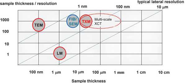
Fig. 1. Sample thickness/resolution for transmission X–ray microscopy (TXM), visual light microscopy (LM), and transmission electron microscopy (TEM), as well as focused ion beam/scanning electron microscopy (FIB/SEM) [6]
The objective of the current study is to analyze and systematize methods of high–resolution XCT for industrial applications. Specifically, the work aims to distinguish the priorities and accuracy requirements of XCT workflows depending on their primary purpose – structure analysis, flaw detection, or quality control – and to clarify how the trade– offs between spatial resolution, acquisition time, and data analysis complexity affect downstream task quality. By analyzing representative nondestructive workflows that combine fast, large–area inspection techniques such as Scanning Acoustic Microscopy (SAM) with high–resolution imaging techniques such as nano–XCT, this study defines pathways for efficient defect inspection and metrology in semiconductor manufacturing. Furthermore, it aims to outline strategies for optimizing image acquisition and reconstruction through algorithmic approaches, including deep learning–based denoising and artefact reduction, thereby supporting the integration of AI/ML–assisted metrology workflows for advanced packaging and heterogeneous integration technologies. The overall goal is to provide a foundation for balancing accuracy, throughput, and reliability in future XCT–based industrial inspection and quality control systems.
1. High–resolution X–ray imaging 1.1. The development of the X–ray tomography method
Roughly two decades after Wilhelm Conrad Röntgen’s discovery of X–rays in 1895, scientists began discussing the idea of layer–by–layer radiographic imaging – a way to visualize individual internal layers without overlapping shadows. Eventually, the radiation itself took the discoverer’s name. Interpreting conventional X–ray images (radiographs) has always been challenging, since the resulting picture represents the combined projection of the entire internal structure through which the rays pass. The moment when it became possible to reconstruct separate layers of an object without physically cutting it open can be regarded as the birth of X–ray tomography.
According to [21], in 1914 the physician K. Mayer from Poznan presented his work “A Heart Radiograph Without Shadowing” at a congress in Lviv, and a few years later, in 1917, the French radiologist Bocage independently developed a similar layer–isolating X–ray technique, for which he obtained a patent in 1921. His approach involved an X–ray tube and a photographic film cassette moving in opposite directions around a stationary subject during exposure. Later, inventors experimented with different motion paths of the source–detector pair to enhance image contrast, and eventually reversed the process – making the object rotate while the X–ray system remained fixed.
Interestingly, in the same year (1917), Johann Radon published his seminal work on the inversion of linear integral transforms, which laid the mathematical foundation for what would become computed tomography (CT) less than fifty years later [22]. The early tomographic techniques were fully mechanical. The term “tomographie” first appeared in papers by Grossman [23 – 25] and Chaoul [26] in 1935. That same year, V.I. Pheoktistov built the first domestic X–ray tomograph in the USSR, followed by designs from S.P. Yanshek, I. S. Ter–Ogonian, and several other Soviet engineers [21].
In 1958, B.I. Korenblyum and co–authors published an article in Izvestia: Physics Series [27] describing a new tomographic technique based on X–ray data recorded at multiple angles – effectively the first hardware–software system for image reconstruction. They formulated the corresponding integral equation and its solution. The image reconstruction process, which contained about 104 elements, took roughly five minutes. The work was initially published in Russian and only translated into English in the 21st century [28].
During his residency in the mid–1960s, Allan Cormack independently developed a Computer–Assisted Tomography (CAT) method [29 – 31]. He carried out experimental measurements on test samples at Tufts University, coining the term “computed tomography.” Although his results initially attracted little attention, interest grew dramatically in 1971 when the EMI scanner, created by Godfrey Hounsfield at Electro Musical Instruments (EMI), entered the market [32]. The first unit was installed at London Hospital, with its software developed by EMI’s own technology laboratory.
As with all new technologies, early CT systems were complex to build and operate. In Western Europe, scanner adoption was gradual – by 1977, there were about 200 units across Europe, 300 in Japan, and roughly 1,000 in the United States [33]. While radiologists were the main users, cardiology and neurology departments soon began employing CT imaging as well. The technology’s complexity required close collaboration between instrument developers and clinical users. Unlike the industrially driven efforts in Britain, the United States advanced both the instrumental and algorithmic aspects of tomography primarily within academic laboratories.
Within six years, CT scanner design evolved rapidly – four distinct generations appeared, each improving acquisition speed and data recording techniques. Higher scan speeds significantly reduced motion artifacts.
The first–generation EMI scanner (1972) – under development since 1967 – required about 9 hours for data collection and 2 hours for reconstruction. By the time it reached market, head scans took only five minutes, later reduced to one minute. It used a single X–ray beam and detector, moving incrementally through 1 –mm steps, then rotating slightly (~0.5°) between passes until completing a 180° sweep.
The second generation (1975) introduced multiple beams and detectors. The EMI CT 1010, for instance, employed eight detectors per layer and could scan two layers in about one minute. Companies such as Siemens in Germany and Medicure in Hungary began producing similar models. However, long scan times still caused artifacts from patient movement, making these designs more suitable for industrial and scientific applications than for clinical imaging.
Later in 1975, the fan–beam geometry reduced scan time to as little as five seconds, marking the third generation. Developed first by Axronics, these scanners used hundreds to thousands of detectors arranged in an arc, rotating continuously with the X–ray tube. This design drastically increased both data volume and acquisition rate.
The fourth generation, designed partly to avoid patent restrictions, placed about a thousand fixed detectors in a full ring around the object while the tube itself rotated. Here, each detector effectively acted as a focal point.
In the USSR, mathematical research on 3D reconstruction from projections was carried out by B.K. Vanstein [34, 35] at the Institute of Crystallography, focusing on macromolecular structure analysis via electron microscopy. By the late 1970s, E.Yu. Vasilieva [36] at the All–Union Research Institute of Radiation Technology developed a pilot plant, and by the early 1980s, I. B. Rubashov supervised the creation of the first Russian–made X–ray CT prototype (CPT–1000), with a patented reconstruction unit [37, 38].
Every tomographic system has its advantages and limitations. Image contrast may be based on transmission, phase, or a hybrid approach. Each configuration demands different projection–collection methods, leading to variations in reconstruction algorithm complexity. Nevertheless, the essential hardware remains the same: an X–ray source, optical focusing system, detector or recording device (historically a photographic film cassette), and a computer that processes the data – an increasingly demanding task.
Third–generation computers and the earliest CT systems emerged simultaneously. Progress in source, detector, and system design aimed to reduce acquisition time, lower radiation dose, and enhance spatial resolution, which has now reached the nanometer scale [39–42].
-
1.2. Categorization of typical applications
As described above, the application range of high–resolution XCT is very broad. Typical applications of this 3D imaging technique can be categorized into 3 groups [2]:
-
• Structure analysis: Creation of 3D digital images of the complete interior structure of an opaque object, e.g., a natural object or an engineered composite or skeleton material (typically for fundamental research),
-
• Flaw detection: Monitoring industrial processes and defect inspection (e.g., in the semiconductor industry), and
-
• Quality control: Observing kinetic processes in objects, in materials synthesis and materials ageing, as well as during product manufacturing and product use, that are important for industrial quality control and reliability engineering.
Laboratory full-field X-ray microscopes operated in the multi-keV range (usually using monochromatic Cr-K a or Cu-K a radiation) have been nearly exclusively established in physics and materials analysis laboratories at universities and research institutes over the previous two decades. However, currently the semiconductor industry is expressing a strong need for high–resolution 3D imaging techniques and tools, particularly for advanced package failure analysis, metrology, and defect inspection (see e.g. [44, 45]). It is expected that lens–based X–ray microscopy and nano–XCT techniques and tools will be pushed to be ready for the semiconductor industry, firstly to support heterogeneous integration schemes and advanced packaging technologies. The major development goal will be to improve the balance between image acquisition time and achievable resolution, as well as to establish new nondestructive workflows suited for the semiconductor industry.
For reliability engineering in the semiconductor industry, knowledge about early imperfections and small–scale defects – in terms of size, shape, and location – and about the kinetics of defect evolution during in–service operation of a product is needed. Particularly, the study of materials ageing and product degradation, e.g., of the kinetics of micro– void growth and microcrack propagation in materials, requires nondestructive characterization techniques with high spatial resolution [46]. High–resolution XCT provides the capability of in–situ studies of reliability–limiting degradation processes in microelectronic products. Based on such studies, appropriate risk mitigation strategies to avoid catastrophic failure can be established. As an example, the growth of microcracks in integrated circuits, e.g., induced during the wafer dicing process, was studied using nano–XCT, and the possibility of controlled steering of microcracks into microchip regions with high fracture toughness was demonstrated. It was shown that specially designed metal structures – so–called guard rings at the rim of the microchip – dissipate energy; consequently, microcrack propagation is efficaciously slowed down and eventually stopped [47].
-
1.3. Accuracy assessment for the 3D reconstruction
The 3 different categories of applications have different requirements for the accuracy of the 3D reconstruction and for the time–to–data [43]. While the highest possible resolution is requested for group 1, data acquisition and data analysis time are essential for group 2. To get high–resolution 3D information of the complete interior structure of an opaque object using lens–based laboratory nano–XCT requires a thorough data analysis, e.g., the application of deep convolutional neural networks (CNN), for denoising and mitigation of artefacts. On the micro– and nanoscale, thermomechanical instability of tool components and object motion, center of rotation misalignment, and inaccuracy in the detector position require computational efforts [48]. Advanced 3D reconstruction methodologies consider these unavoidable effects during the image acquisition [49].
In [43], a model–based accuracy assessment of reconstruction algorithms used in high–resolution XCT is proposed for the 3 groups of applications as mentioned above, e.g., structure analysis, flaw detection, and quality control. It is a systematic approach to get objective criteria for evaluating the reconstruction accuracy from projections collected under special conditions (parameters of the measurement protocol). Very important for the decision–making process in industry (application groups 2 and 3) is that the accuracy criteria for the reconstruction algorithms are supplemented with outputs from the decision system itself.
A widely used evaluation approach relies on human perception. This approach does not require an ideal image for comparison or the alignment of images. It is based on expert assessment (from individuals or groups). Quantitative indicators for testing on a target audience may use the MOS (Mean Opinion Score) or the R–factor. The accuracy assessment can be based on specific criteria (e.g., blurriness, noise, artifacts). This approach is recommended if results will be visually checked by an operator. Objective accuracy assessments, i.e., those not requiring expert evaluation, can either rely on reference (ideal) images or not. Often, in tomography, reference images are those reconstructed from projections of a phantom (a synthetic object with known properties, e.g., an objective quality standard (“golden sample”) in the semiconductor industry) obtained in ideal conditions. Ideal conditions assume many projection angles satisfying the Whittaker–Kotelnikov–Shannon (WKS) sampling theorem and high signal–to–noise ratios.
Standard quality metrics for objective assessment include [50]:
-
• MSE (Mean Square Error): Measures the average squared difference between pixel values of the phantom and the reconstructed image.
-
• PSNR (Peak Signal-to-Noise Ratio): Evaluates the degree of difference from the reference image.
-
• SSIM (Structural Similarity Index Measure): Quantifies structural similarity.
Often, several metrics are used together for comprehensive assessment since different algorithms may introduce different types of noise and artifacts.
The objective assessment of the accuracy of the tomographic reconstruction is different for the 3 groups of applications categorized above [43]:
Structure analysis: Total voxel brightness deviations from the reference (MSE, PSNR, SSIM) are measured or, if the phantom is missing, the projection error.
• Flaw detection: (a) A combined error, including pixelwise brightness difference and model-based difference in a defect parameter space; weights are set empirically. This can focus on the region containing the defect, i.e., detection, comparison with a defect model, and reject/accept decision. (b) A structure–oriented wavelet approach: accuracy is assessed in the wavelet domain at relevant scales (e.g., for form error or local area size deviations).
• Quality control: Reconstruction accuracy must be evaluated concerning the requirements of downstream steps such as motion modeling, automatic unrolling, or character recognition.
2. Application of nano–XCT in microelectronics
2.1. Heterogeneous integration of microchips and chiplet architectures2.2. Nondestructive workflows for defect inspection
The semiconductor industry has been a unique industry for several decades, and it has been a major technology driver, continuously inducing innovations. New applications such as cloud–based applications, data mining, artificial intelligence (AI), and future cars, and the resulting more–than–ever demand for high–performance computing, connected with low power, low latency, and low cost, forced designers to new solutions: heterogeneous integration of chips and chiplet architectures. Hybrid bonding (HB), a technology for vertical (3D) stacking of microchips, is expected to be the most transformative innovation to semiconductor manufacturing since the introduction of EUV lithography. Instead of solder microbump interconnects with high resistance, several microchips or wafers are directly connected with Cu through– silicon vias (TSVs), resulting in low–resistance and consequently low–power copper–to–copper connections [51,52]. The very stringent requirements on HB – surface smoothness, cleanliness, and bond alignment accuracy to achieve high– quality bonds – cause challenges to metrology and defect inspection [53]. Monitoring the alignment of metal structures is a demanding task for HB metrology. Wafer–to–wafer (W2W) processes offer higher alignment accuracy, throughput, and bond yields than die–to–wafer (D2W) processes. However, advanced metrology techniques to monitor the alignment accuracy are needed for both process flows. This task becomes more and more challenging with the downscaling of the interconnect sizes. Infrared (IR) scanners to check the alignment quality can only be used if one wafer is transparent for photons in the IR range. Since this requirement is not fulfilled for CMOS wafers with metal interconnects and for backside power delivery architectures, other techniques such as nano–XCT have to be applied.
There is a strong need for high–resolution 3D imaging techniques and tools, particularly for physical failure analysis, defect inspection, and metrology of advanced packaging technologies [44,45]. The EDFAS roadmap [54] is addressing the need to improve the resolution of 2D and 3D X-ray imaging to the sub- y m level to detect and classify defects in interconnects such as through–silicon–vias (TSVs), e.g., micro–voids, and at hybrid bonding interfaces, e.g., particles. Efforts are needed before the X–ray inspection methodology is introduced to production lines, and until inspection of a high volume of microchips and heterogeneously integrated chiplets is a reality. The application of nano–XCT as a highly reliable inspection method requires a balance between throughput and fault detection (i.e., measurement and reconstruction accuracy) [54]. Ways for a drastic increase in acquisition speed without sacrificing the resolution of the X–ray images are high–brilliance laboratory X–ray sources, the application of AI/ML algorithms for new image acquisition protocols in industrial applications, and high–speed data processing. A dynamical adjustment of the measurement protocol in real–time (including the use of decision–making thresholds or so–called stopping rules) will reduce the data acquisition time and enable feedback within the manufacturing process (see e.g. [49,55]).
In addition to the need to improve the balance between image acquisition time and achievable resolution for high– resolution X–ray imaging, a major development goal is to establish new nondestructive workflows suited for the semiconductor industry [56]. Such workflows are supposed to combine a high–throughput technique that identifies a region of interest (ROI) – e.g., scanning acoustic microscopy (SAM) or quantum diamond microscopy (QDM) – with a high–resolution 3D imaging technique – e.g., nano–XCT. One potential example, as demonstrated in Fig. 2, is a seamless nondestructive workflow for defect inspection, e.g., for advanced packaging technologies, that combines acoustic and X– ray techniques (SAM and nano–XCT) to auto–detect and auto–classify defects, to improve throughput and defect detectability [6, 56].
SAM, characterized by a scan speed that is much higher than that for high–resolution XCT, provides information about surface and sub–surface discontinuities in a material or system, and therefore, it is the technique of choice for inspecting interfacial integrity (e.g., delamination) and for detecting defects (e.g., voids, cracks) in bonded wafers [57,
-
58] . However, conventional SAM techniques have a trade–off in penetration depth and resolution. They are reaching limits for 3D–stacked chiplets, since highly penetrating low–frequency acoustic waves are unable to provide the resolution needed for advanced packaging technologies. Fault isolation and defect inspection for advanced packaging with high– density sub y m interconnects require a spatial resolution of 500 nm and below. In addition, the convolution of signals from various die interfaces makes it difficult to select the correct signal for rendering the right image from the interface of interest. Several beyond state–of–the–art approaches are addressing these challenges, particularly high–frequency SAM. The detection of voids in TSVs applying the GHz–SAM technology was demonstrated in [59, 60]. SAM
interferometry, where the defocused sound field induces surface–acoustic–waves, provides unique interference patterns associated with the quality of each TSV. Finally, a fully automated, highly efficient end–to–end convolutional neural network (CNN) model can classify thousands of TSVs and provide statistical information [61]. SAM can be used in a nondestructive workflow to identify a ROI, where nano–XCT can be applied to visualize defects in metal interconnects and package structures such as TSVs, Copper pillars, and solder microbumps with high resolution within the ROI [62, 63]. It has to be mentioned that nano–XCT in the hard X–ray regime, i.e., for photon energies > 10 keV, is needed to avoid destructive sample preparation steps before imaging structures and defects in microchips or packaged systems [64].
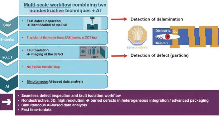
Fig. 2. Nondestructive workflow for buried defect detection, combining SAM and nano–XCT, for Hybrid Bonding technology [56]
In practical scenarios [56, 65], in such a combined nondestructive workflow, SAM serves as the fast, large–area inspection method for locating regions of interest, while nano–XCT provides detailed three–dimensional visualization of the detected defects at nanoscale resolution. SAM imaging of bonded wafer pairs reveals interfacial delamination, voids, and other imperfections as regions of dark contrast in the acoustic micrographs, where the absence or attenuation of reflected ultrasonic signals indicates poor adhesion or “kissing bonds”. In the case of polymer–based bonding layers such as benzocyclobutene (BCB), SAM can also identify characteristic dendrite–like defect patterns that form due to irregular polymer crystallization during solvent cooling (Fig. 3).
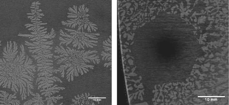
Fig. 3. Dendrite–like patterned (left) and kissing bond (right) are observed in the SAM data of the non–patterned BCB bonded wafer pair [65]
These dendritic structures become more pronounced with increasing molecular weight of the polymer, reflecting variations in local crystallization kinetics. The acoustic microscope is particularly sensitive to such morphological irregularities because they locally alter the acoustic impedance, producing distinct contrast variations in C–scan images. The use of high–frequency transducers (typically 100 MHz and above) allows the inspection of thinned wafers with top– layer thicknesses between 100 µm and 400 µm, enabling depth–resolved C–scans and approximate layer thickness measurements. By improving wafer edge sealing during scanning, artifacts caused by coupling medium intrusion can be minimized, thereby enhancing the reliability of acoustic defect detection and ensuring more accurate mapping of the bonding interface.
After the acoustic inspection step, the regions identified by SAM are further analyzed using nano–XCT. This technique reconstructs the three–dimensional internal structure of the selected sub–volume by acquiring X–ray projections at multiple angles, providing volumetric datasets with voxel sizes down to tens of nanometers. In the case of advanced packaging, such as copper–filled TSVs, nano–XCT reveals not only the presence of voids but also their exact geometry, volume, and position within the interconnects. For example, large voids may appear at the bottom of 4 µm TSVs, while smaller central voids are typically observed in 5 µm TSVs near their upper sections (Fig. 4). These 3D reconstructions enable precise quantification of defect morphology and spatial distribution without destructive cross–sectioning or polishing.
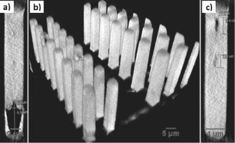
Fig. 4. a) 2D image shows a huge void at the bottom of 4 µm TSV, b) The 3D tomography of 4 and 5 µm TSVs and c) 2D image shows voids close to the top of 5 µm TSV [65]
The combination of SAM and nano–XCT therefore provides a complementary and hierarchical diagnostic workflow. SAM rapidly screens the entire wafer or package surface to localize potential defects, and nano–XCT then targets those regions for high–resolution quantitative analysis. Together, these methods allow both high–throughput inspection and nanoscale defect characterization within the same nondestructive workflow. This integration of acoustic and X–ray microscopy forms a foundation for future automated inspection pipelines in semiconductor manufacturing, where artificial intelligence can further enhance defect recognition, classification, and process feedback.
Conclusion
In this paper, complementing several existing reviews focused on XCT workflows [66 – 68] and extending them toward an in–depth analysis of approaches to understanding and quantifying reconstruction quality, the typical industrial applications of high–resolution X–ray computed tomography (XCT) are analyzed, structured, and classified into three main categories: (1) structure analysis, (2) flaw detection, and (3) quality control. These different categories of applications have different requirements for the accuracy of the 3D reconstruction and for the time–to–data. Limitations on time or memory may require algorithm optimization, affecting accuracy; thus, accuracy assessment is a key task. While the highest possible resolution is requested for group 1, data acquisition and data analysis time are essential for group 2. High–resolution XCT provides the capability of in–situ studies of kinetic processes (group 3), e.g., reliability–limiting degradation processes in microelectronic products. Based on such studies, appropriate risk mitigation strategies to avoid catastrophic failure can be established. The accuracy of the 3D information from nano–XCT of an opaque object depends on the number of data, e.g., the number of projections and the data acquisition time per projection, and on the data analysis, e.g., the application of deep convolutional neural networks, for denoising and mitigation of artefacts.
The application of high–resolution X–ray imaging techniques for industrial process and quality control is forced by the need to detect flaws in advanced micro– and nano–structured materials and high–tech products manufactured with nanotechnologies. New developments and innovations in metrology and inspection (MI) will enable the semiconductor industry to control process steps and to identify defects faster and with higher accuracy than before, an urgent need for future CMOS technology nodes and in vertically stacked chiplets with high-density sub- ц т 3D interconnects. New metrology solutions will support developing and ramping up new advanced packaging technologies, which are characterized by further feature shrinking and the integration of novel materials, as well as for continuous yield improvement.
The EDFAS roadmap [54] is addressing the need to improve the resolution of 2D and 3D X–ray imaging to the sub– ц т level to detect and classify defects in interconnects and at hybrid bonding interfaces. Efforts are needed before the X-ray inspection methodology is introduced to production lines, and until inspection of a high volume of microchips and heterogeneously integrated chiplets is a reality. One important aspect is the integration of AI/ML algorithms into the MI tools, to adjust the measurement protocol dynamically in real–time, reducing data acquisition time and enabling actions in the manufacturing process before the yield is affected. This new approach will have important implications for risk mitigation strategies in the semiconductor industry and for the manufacturing of microchips that will be used in reliable and sustainable high–tech products.
Advanced workflows for process monitoring and accurate, efficient defect detection and classification in the semiconductor industry will combine multiple analytical techniques with different spatial resolution and throughput, complemented by advanced data analysis utilizing artificial intelligence (AI) and machine learning (ML) algorithms. For advanced packaging, and particularly for the hybrid bonding (HB) technology, a seamless workflow for defect inspection that combines acoustic and X–ray techniques to auto–detect and auto–classify defects, to improve throughput and defect detectability, is proposed [56].
Referenes
About authors
Ehrenfried Zschech was born in Auritz (Saxony), Germany, in 1956. He graduated TU Dresden, Saxony, Germany in solid state physics in 1979, and received the Dr. rer. nat. habil. degree in 1988 in the same university. He is a profeesor, winner of multiple prestigious awards and honorary member of multiple scientific associations.
He has an h–index 45 with over 400 publications in peer–reviewed journals and over 10000 citations. His research interests include but not limited to material science, x–ray technologies, semiconductors and solid state physics.
