Implementation of An Optimized and Pipelined Combinational Logic Rijndael S-Box on FPGA

Author: Bahram Rashidi, Bahman Rashidi
Journal: International Journal of Computer Network and Information Security(IJCNIS) @ijcnis
Article in issue: 1 vol.5, 2013.
Free access
In this paper, presents an optimized combinational logic based Rijndael S-Box implementation for the SubByte transformation(S-box) in the Advanced Encryption Standard (AES) algorithm on FPGA. S-box dominated the hardware complexity of the AES cryptographic module thus we implement its mathematic equations based on optimized and combinational logic circuits until dynamic power consumption reduced. The complete data path of the S-box algorithm is simulated as a net list of AND, OR, NOT and XOR logic gates, also for increase in speed and maximum operation frequency used 4-stage pipeline in proposed method. The proposed implemented combinational logic based S-box have been successfully synthesized and implemented using Xilinx ISE V7.1 and Virtex IV FPGA to target device Xc4vf100. Power is analized using Xilinx XPower analyzer and achieved power consumption is 29 mW in clock frequency of 100 MHz. The results from the Place and Route report indicate that maximum clock frequency is 209.617 MHz.
Rijndael S-box, Combinational logic, Pipelining, FPGA, VHDL
Short address: https://sciup.org/15011154
IDR: 15011154
Text of the scientific article Implementation of An Optimized and Pipelined Combinational Logic Rijndael S-Box on FPGA
Cryptography is the science of information and communication security. Cryptography is the science of secret codes, enabling the confidentiality of communication through an insecure channel. It protects against unauthorized parties by preventing unauthorized alteration of use. It uses a cryptographic system to transform a plaintext into a cipher text, using most of the time a key [1]. Byte substitution and Inverse Byte Substitution are the most complex steps in the encryption and decryption processes. In these steps each byte of the state array will be replaced with its equivalent byte in the S-box or the Inverse S-box. As AES algorithm use elements within the GF (28), each element in the state array represents a byte with a value that varies between 00H-FFH. The S-box has a fixed size of 256 bytes represented as (16*16) bytes matrix [2]. In this paper propose an optimized and pipelined architecture for S-box block in AES based on combinational logic. We used minimum number of logic gate in proposed design. In recent years, a number of researches have been proposed for Implementation of S-box by using the FPGA by [317]. In continue we present some researches, in [3], a software method of producing the multiplicative inverse values, which is the generator of S-box values and the possibilities of implementing the methods in hardware applications will be discussed. The method is using the log and antilog values. The method is modified to create a memory-less value generator in AES hardware-based implementation. In [4], they propose an improved masked AND gate, in which the relationship between inputs masked values and masks, is nonlinear. Usually, when converting S-box operations from GF (28) to GF (((22)2)2), all the necessary computations become XOR and AND operations. Therefore, to fully mask AES S-box is to substitute the unmasked XOR and AND operations with the proposed masked AND gate and protected XOR gate. In [5], a general method for sharing common subexpressions derived from the algebraic finite fields is proposed. Furthermore, they present a randomly configurable architecture for protecting S-box transformation. [6], presents a compact implementation of the S-box of Pomaranch stream cipher using composite field arithmetic in GF ((23)3). It describes a systematic exploration of different choices for the irreducible polynomials that generate the extension fields. It also examines all possible transformation matrices that map one field representation to another. In [7], they propose countermeasure techniques for AES with S-box hiding using four different implementations of S-boxes using composite fields. The proposed work by [8], employs a combinational logic design of S-box implemented in FPGA. The architecture employs a Boolean simplification of the truth table of the logic function with the aim of reducing the delay. The S-box is designed using basic gates such as AND gate, NOT gate, OR gate and multiplexer. In [9], presents FPGA implementation and overhead evaluation for an algorithmic Differential Power Attack (DPA) countermeasure for AES. In [10], presents a new efficient method for implementation of the AES byte substitution function. It is aimed at the AES implementation in non-volatile FPGAs featuring volatile embedded RAM blocks. The method uses a pair of linear feedback shift registers to generate substitution tables into embedded RAMs. The proposed solution requires less space and is faster than the one implementing whole S-boxes in the logic area, and it is especially suited to a power-aware AES implementation. In[11], investigate a new compact digital hardware implementation of AES Structure with integrated S-box and Inverse S-box transformation which minimizes the computation cost of the relevant arithmetic in the finite field GF (28), including the cost of the mapping. This approach has advantages over a straightforward implementation using read-only memories for table lookups. The resulting S-box design with subfield operations in GF ((((22)2)2 offers a reduction in the reconfigurable logic by 81% low gate count as compared to Look Up Table(LUT) and 23% better performance in area and faster by 3% in comparison with one using GF ((24)2). A high speed architecture for composite field arithmetic based S-boxs transformation used in AES is present by[12]. In [13], two instructions for S-box access are designed by constructing a novel flexible on-chip parallel substitution box unit that consists of multiple LUT and a postprocessing module. The box unit is integrated into the 32-bit configurable Leon2 processor. Configuration of Leon2 is presented. Implementing this extended processor core on FPGA shows that the parallel substitution box unit uses very small amount of hardware resources. The proposed architecture is derived by extending the precomputation technique suggested recently by Liu and Parhi [14] to a recently proposed architecture of AES S-box due to Rashmi, Mohan and Anami [15]. To reduce implementation overhead the masked compact S-box, proposed by Canright [16], was chosen to implement a DPA countermeasure on an SRAM FPGA. This paper is organized as follows. In section II description of the subbyte transformation, proposed method and proposed architecture is presented. Section III discusses comparison of the hardware implementation and chip utilization taken from Xilinx ISE that verifies the performance of the proposed work. Section IV is the conclusion.
-
II. The SubByte Transformation
Paper presents a combinational logic based Rijndael S-box implementation for the Sub Byte transformation in the AES algorithm for FPGA. We for implementation S-box use from [17-18]. Using combinational logic for implement S-box has small area occupancy and high throughput, and as compared to the typical ROM based LUT implementation which access time is fixed and unbreakable. The SubByte transformation is computed by taking the multiplicative inverse in GF (28) followed by an affine transformation [17].
SubByte:
-
1- Multiplicative Inversion in GF (28)
-
2- Affine Transformation
The Affine Transformation can be represented in matrix form and it is shown below:
" 1
1
1
1
1
0
0
0"
" a 7"
"0"
0
1
1
1
1
1
0
0
a 6
1
0
0
1
1
1
1
1
0
a 5
1
AT ( a ) =
0
1
0
0
0
0
1
0
1
1
1
1
1
1
1
1
x
a 4
a 3
©
0
0
1
1
0
0
0
1
1
1
a ^
0
1
1
1
0
0
0
1
1
a 1
1
L 1
1
1
1
0
0
0
1 J
L a o J
L 1 J
The AT is the Affine Transformation From here, it is observed that the SubByte transformation involve a multiplicative inversion operation. This section illustrates the steps involved in constructing the multiplicative inverse module for the S-box using composite field arithmetic. The multiplicative inverse computation will first be covered and the affine transformation will then follow to complete the methodology involved for constructing the S-box for the SubByte operation. The individual bits in a byte representing a GF (28) element can be viewed as coefficients to each power term in the GF (28) polynomial. For instance, {10001011} 2 is representing the polynomial q7 + q3 + q + 1 in GF (28). From [18], it is stated that any arbitrary polynomial can be represented as bx + c , given an irreducible polynomial of x2+Ax+B . Thus, element in GF (28) may be represented as bx+c where b is the most significant nibble while c is the least significant nibble. From here, the multiplicative inverse can be computed using the equation below [18].
(bx+c)-1 = b (b2 B+bcA+c 2) 1 x+(c+bA)(b2 cA+c 2) 1
From [17], the irreducible polynomial that was selected was x2+x +λ . Since A=1 and B= λ , then the equation could be simplified to the form as shown below [17].
(bx+c)-1 = b(b2X+c(b+c))1 x+(c+b)(b2X+c(b+c) )1
The above equation indicates that there are multiply, addition, squaring and multiplication inversion in GF (24) operations in Galois Field. Each of these operators can be transformed into individual blocks when constructing the circuit for computing the multiplicative inverse. From this simplified equation, the multiplicative inverse circuit GF (28) can be produced as shown in Fig.1.
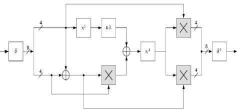
Fig.1: Multiplicative inversion module for the S-box.
The legends for the blocks within the multiplicative inversion module from above are illustrated in Table I.
a6
a5 a4
a3
a2
a1
Fig.2: Proposed implementation of the affine transformation.
Table I: Legends for the building blocks within the multiplicative inversion module.
|
5 |
Isomorphic mapping to composite fields |
|
x2 |
Squarer in GF(24) |
|
x-1 |
Multiplication inversion in GF(24) |
|
5 -‘ |
Inverse isomorphic mapping to GF(28) |
|
x X |
Multiplication with constant, in GF(24) |
|
® |
Addition operation in GF(24) |
|
X |
Multiplication operation in GF(24) |
-
2) Isomorphic Mapping and Inverse Isomorphic Mapping
The multiplicative inverse computation will be done by decomposing the more complex GF(28) to lower order fields of GF(21), GF(22) and GF((22)2). In order to accomplish the above, the following irreducible polynomials are used [14].
GF(22) ^ GF(2) : x2 + x +1GF((22)2)^GF(22) :x2 + x + ф (1)GF (((22)2)2) ^ GF ((22)2) : x2 + x + X
Where φ = {10} 2 and λ = {1100} 2 . Computation of the multiplicative inverse in composite fields cannot be directly applied to an element which is based on GF (28). That element has to be mapped to its composite field representation via an isomorphic function, δ. Likewise, after performing the multiplicative inversion, the result will also have to be mapped back from its composite field representation to its equivalent in GF(28) via the inverse isomorphic function, δ-1. Both δ and δ-1 can be represented as an 8*8 matrix. Let q be the element in GF(28), then the isomorphic mappings and its inverse can be written as δ*q and δ-1*q, which is a case of matrix multiplication as shown in below , where q 7 is the most significant bit and q 0 is the least significant bit [17]. Proposed implementation of the affine transformation is shown in Fig.3.
The matrix multiplication can be translated to logical XOR operation. The logical form of the matrices above is shown below.
q 7
q 7 ® q 6 ® q 4 ® q з ® q 2
q 7 ® q 5 ® q 3 ® q 7 ® q 5 ® q 3 ® q 2 ® q 7 ® q 6 ® q 2 ® q 7 ® q 4 ® q 3 ® q 2 ® q, q 6 ® q 4 ® q 1 q 6 ® q 1 ® q 0
q 7 ® q 6 ® q 5 ® q 1
q 6 ® q 2
q 6 ® q 5 ® q 1
q6 ® q5 ® q4 ® q2 ® q1 q ®q ®q ®q ®q q ®q ®q ®q ®q q6 ® q4
q 6 ® q 5 ® q 4 ® q 2 ® q 0
As seen in above matrix this block is implementation based on XOR gates . We for implementation of this block use minimum number of XOR gates, until proposed design optimized. Also other blocks in S-box are designed with combinational logic implemented with minimum number of logic gates. Proposed implementation of δ*q is shown in Fig.3.
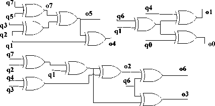
Fig.3: Proposed implementation of δ*q.
Also proposed implementation of δ-1*q is shown in Fig.4.
q1
q5
o3 q6
q3
q6
q5
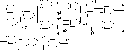
q2
q q7
Fig.4: Proposed implementation of δ-1*q.
From [18] and [19], any arbitrary polynomial can be represented by bx+c where b is upper half term and c is the lower half term. Therefore, from here, a binary number in GF q can be spilt to q H x+q L . For instance, if q={1011} 2 , it can be represented as {10} 2 x+{11} 2 , where q H is {10} 2 and q L = {11} 2 . q H and q L can be further decomposed to {1} 2 x+{0} 2 and {1} 2 x+{1} 2 respectively. Using this idea, the logical equations for the addition, squaring, multiplication and inversion can be derived.
-
3) Squaring in GF(24)
Let k =q2, where k and q is an element in GF(24), represented by the binary number of {k 3 k 2 k 1 k 0 } 2 and {q 3 q 2 q 1 q 0 } 2 respectively.
The k L term is also decomposed in the similar manner as shown below.
kL = ( q з x + q 2) 2 ({1}2 x + 0) + ( q 1 x + q о )2
kL = q H 2 ф + b L 2 = ( q з q 2 ) 2{1 0} 2 + ( q 1 q о) 2
kL =(q 32x 2 + q 2 q 3x+q 2 q 3x+q 22)(x) +
(q12 x2 + q 0 q1x+q 0 q^x+q о2)2 {10}2+ (q^ q о)2
kL = qHx3 + q2x + qxx2 + q0
As was done earlier, the x2 term can be substituted since x2=x+1 . For the case of x3 , it can be obtained by multiplying x2 by x . That is, x3=x(x)+x=x2+x . Substituting for x2 , x3=x+1+x. The two x terms cancel out each other, leaving only x3=1 . Performing this substitution to the above expression yields the following.
kL = q 3(1) + q 2 x + q 1( x + 1) + q о
k1^ + k0 = (q2 + q^x + (q3 + q1 + q0) e GF(2) (3)
From equations (2) and (3), the formula for computing the squaring operation in GF (24) is acquired as shown below.
( A
k =
k 3 к 2 k 1 k 0
1—.—”—.—1
V k H kL J
= kHx + kL
( ) 2
q з q 2 q 1 q о
*------v------11------V------'
V q H q L J
= (qHx + qL )2
22 2 22 2
kL = q H x + q H q L x + q H q L x + q L = q H x + q L
k3 = q 3
k2 = q 3 ® q 2
k1 = q 2 ® q 1
k0 = q 3 ® q 1 ® q о
k=qH (x+ф)+qL
Proposed implementation of above equations is shown in Fig.5.
к = qH2 x + (qHф+qL2 )e GF (22)
^^ ■'
kH
^^
K L
i0
o3
i3
o2
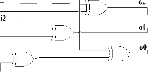
Fig.5: Proposed implementation of Squarer in GF(24).
The expression above is now decomposed to GF (22). Decomposing k H and k L further to GF (2) would yield the formula to compute squaring operation in GF (24).
kH = q H = ( q 3 q 2 ) = ( q 3 x + q 2 )
22 2 2
kH = q3 x + q3q2x + q3q2x + q2 = q3x + q2
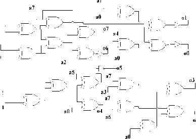
4) Multiplication with constant, λ
Let k = qλ, where k= {k 3 k 2 k 1 k 0 } 2 , q= {q 3 q 2 q 1 q 0 } 2 and λ= {1100} 2 are elements of GF (24).
Using the irreducible polynomial from (1) x2 +x+1, and setting it to x2=x+1, x2 is substituted and the new expression is obtained.
kH = q 3( x + 1) + q 2
k3x + k2 = q3x + (q2 + q3) e GF(2) (2)
k =
k 3 k 2 k 1 k о
*—v—”—v—*
V kH kL J
= kHx + k,
HL
r )
q 3 q 2 q 1 q 0 ‘————————' V qH qL J
r ) 1100 ——
V ^ H ^ L J
k = ( q H x + q L )( ^ hx + ^ l )
Modulo reduction can be performed by substituting х2=х+ф using the irreducible polynomial in (4) to yield the expression below.
-
k = q H A h ( x + ^ + q ^ ^ H x
-
k = GbA + q l A h , ) x + q A h H e GF ( 22 ) kH kL
The k H and k L terms can be further broken down to GF(2).
-
kH = q H A H + qL A H
k = ( q 3 q 2)(112) + ( q 1 q o )(112)
kH = ( q3x + q 2)( x + 1) + ( qx + q 0)( x + 1)
-
kH = q 3 x 2 + ( q 3 + q 2 ) x + q 2 + q 1 x 2 + ( q 1 + q 0 ) x + q 0
o1
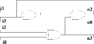
Fig.6: Proposed implementation of multiplication with constant λ.
5) GF(24) Multiplication
Let k = qw, where k= {k3 k2 k1 k0}2, q = {q3 q2 q1 q0}2 and w = {w 3 w 2 w 1 w 0 } 2 are elements of GF (24).
k =
Substituting x2=x+1, would then yield the following.
kH = q 3( x + 1) + ( q 3 + q 2 ) x + q 2 + q 1( x + 1) + ( q 1 + q 0 ) x + q 0
kH = ( q 3 + q 3 + q 2 + q 1 + q 1 + q 0 ) x + ( q 3 + q 2 + q 1 + q 0 )
k3 x + k2 = ( q 2 + q 0) x + ( q 3 + q 2 + q + q 0) e GF (2) (4)
The same procedure is taken to decompose kL to GF (2). kL =qHАнФ kL = (q 3 q 2)(112)(102)
kL = ( q3x + q 2)( x + 1)( x )
kL = q3x 3 + q2x 2 + q3x 2 + q2x
Again, the x2 term can be substituted since x2=x+1 .
Likewise, x3 is also substituted with x3=1, kL = q 3(1)+q 2(x+1)+q 3(x+1)+q 2x kL =(q 3+ q 2+ q 2)x+(q 3+ q 3+ q 2) (5)
k 1 x + k 0 = ( q 3) x + ( q 2) e GF (2)
From equations (4) and (5) combined, the formula for computing multiplication with constant λ is shown below.
k3 = q 2 ® q о k2 = q3 Ф q2 Ф q1 Ф q0
k1 = q 3
k o = q 2 (6)
Proposed implementation of multiplication with constant λ is shown in Fig.6.
k3k2 k 1 k 0
^^^H
\ k H kL /
= kHx + kL
q 3 q 2 q 1 q 0
^H^H к qH qL У
HH к wH w )
= ( q H x + q L )( w H x + w L )
k = ( q H w H)(x + ^ ) + ( q H w L + q L w H)x + q L w L
Substituting the x2 term with x2 = x + φ yields the following.
k = ( q H w H ) x 2 + ( q H w L + q L w H ) x + q L w L
k=kHx+kL = (qHwH+qHwL+qLwH)x
+ q H w H ^ + q L w L e GF( 22 ) (7)
Equation (7) is in the form GF (22). It can be observed that there exist addition and multiplication operations in GF (22). Addition in GF (22) is but bitwise XOR operation. Multiplication in GF (22), on the other hand, requires decomposition to GF (2) to be implemented in hardware. Also, it the expression would be too complex if equation (7) were to be broken down to GF (2). Thus, the formula for multiplication in GF (22) and constant φ will be derived instead. Fig.7 below shows the hardware implementation for multiplication in GF (24).
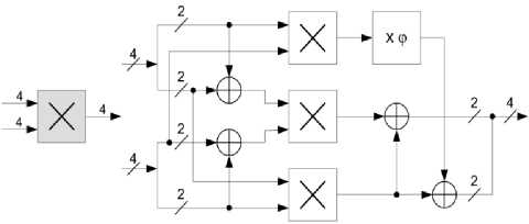
Fig.7: Hardware implementation of multiplication in GF (24).
6) GF(22) Multiplication
Let k=qw, where k = {k 1 k 0 }2, q= {q 1 q 0 } 2 and w = {w 1 w 0 } 2 are elements of GF (22).
k = (k1ko ) = k 1 x + k o = ( q 1 q o)(w1wo ) = ( q 1x + q o)(w1x + wo )
k = q1w1x2 + q o w3x + q 1wox + q o w o
The x2 term can be substituted with x2=x+1 to yield the new expression below.
k=qiwi(x+1)+qowix+qiwox+qowo kix+ko = (qiwi+qowi + qiwo)x
+ ( q iwi + q o w o ) e GF(2) (8)
The equation above can now be implemented in hardware as multiplication in GF (2) involves only the use of AND gates. That we use from AND gate for its implementation. The formula for computing multiplication in GF (2) is as follows.
ki = qiwi ® qowi ® qiwo ko = qiwi ® qowo (9)
Fig.8 illustrates its hardware implementation.
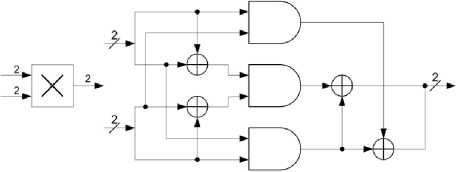
Fig.8: Hardware implementation of multiplication in GF (22).
The above hardware implementation is different of the (9) for the computation of k 1 . It can be proven that the implementation above for computing k 1 would result to the expression in (9), as shown below.
ki =(qi ® q o)(wi ® wo) ® (qowo)
ki =(qiwi) ®(qowi) ®(qiwo) ®(qowo) ®(qowo)
ki =(qiwi) ® (qowi) ® (qiwo)
-
7) Multiplication with constant φ
Let k=qφ, where k = {k 1 k 0 } 2 , q = {q 1 q 0 } 2 and φ = {10} 2 are elements of GF(22).
k = kix+ko = (qiqo)(io2) = (qix + qo)(x)
Substitute the x2 term with x2=x+1 , yield the expression below.
kj = qxx2 + qox
k = q/x + i) + q0 x k = (qi + qo) x + (qi) e GF(2) (io)
From (10), the formula for computing multiplication with φ can be derived and is shown below.
ki = qi ® qo ko = qi
The hardware implementation of multiplication with φ is shown below in Fig.9.
Fig.9: Hardware implementation of multiplication with constant φ.
-
8) Multiplicative Inversion in GF(24)
In [19] has derived a formula to compute the multiplicative inverse of q (where q is an element of GF (24)) such that q-1={q 3 -1,q 2 -1,q 1 -1,q 0 -1} The inverses of the individual bits can be computed from the equation below [19].
Я 3 - i = q 3 ® q 3 q 2 q i ® q 3 q o ® 4 2
4 2 - i = 4 з q 2 q i ® q 3 q 2 q o ® q 3 q o ® q 2 ® q i q 2
4 i - 1 = 4 з ® 4 з 4 2 4 1 ® 4 з 4 1 q o ® q 2 ® q 2 4 o ® q i
4 o - i = 4 з q 2 q i ® 4 3 4 2 4 o ® 4 з 4 1 ® q 3 q i q o ® q 3 4 o ® q 2
®q2q, ®q^q^Q ®q[ ® q0
Proposed implementation of these equations is shown in Fig.10.
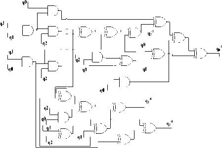
Fig.10: Proposed implementation of Multiplicative Inversion in GF (24)
As explained proposed implementation for S-box is based on pipelining until performance and speed is increased. Fig.11 shows proposed pipelined S-box.
Fig.11: Proposed pipelined S-box.
-
IV. comparison
We design a FPGA implementation of the S-box algorithm based on combinational logic. In this paper proposed method has been written by VHDL hardware description language. In order to get actual numbers for the hardware usage this work was synthesized and implemented using Xilinx 7.1 software, Virtex-4 FPGA to target device Xc4vfx100 also power is analyzed using Xilinx XPower analyzer. Table II shows utilization hardware and performance in different works and proposed method for S-box also Table III shows power consumption in proposed method for S-box.
Table III: Power consumption in proposed method for S-box.
|
Clock(MHz) |
25 |
50 |
75 |
100 |
|
Power(mW) |
20 |
23 |
26 |
29 |
Table II: Comparisons of hardware utilization and performance
-
V. conclion
The aim of paper is design and implementation of the optimized combinational logic based Rijndael S-Box on FPGA. Proposed method is based on combinational logic, thus it is low power and number of logic gates is very low. The approach used for increase performance is pipelining technique we use 4-stage pipelining in S-Box design. The proposed architecture only is based on XOR, AND, NOT, and OR logic gates. This method has more speed and low power than other work.
References Implementation of An Optimized and Pipelined Combinational Logic Rijndael S-Box on FPGA
- Aseem Jagadev, "Advanced Encryption Standard (AES) Implementation", Bachelor of Technology THESIS, Department of Electronics and Communication Engineering National Institute of Technology, Rourkela, May, 2009.
- Issam Mahdi Hammad, "Efficient Hardware Implementations For The Advanced Encryption Standard (AES) Algorithm" Master Thesis, Dalhousie University Halifax, Nova Scotia 2010.
- Naziri, S.; Idris, N., "The memory-less method of generating multiplicative inverse values for S-box in AES algorithm", Electronic Design, ICED. IEEE International Conference, 2008, pp. 1-5.
- Zeng, Juanli et al, "Improvement on masked S-box hardware implementation", Innovations in Information Technology (IIT), IEEE International Conference, 2012, pp 113-116.
- Jun-Hong Chen et al; Ming-Der Shieh, "Exploration of Low-Cost Configurable S-box Designs for AES Applications", Embedded Software and Systems, ICESS '08. IEEE International Conference, 2008, pp. 422-428
- Ebrahimi Atani et al, "Low cost implementation of Pomaranch S-Box", Wireless Communication, Vehicular Technology, Information Theory and Aerospace & Electronics Systems Technology, Wireless VITAE, IEEE International Conference, 2009, pp. 875-879.
- Jae Seong Lee et al, "S-box hiding methods for AES hardware chips against differential power analysis based on composite field", Network Infrastructure and Digital Content, 2nd IEEE International Conference on, 2010, pp. 778-782.
- Ahmad, N et al, "Design of AES S-box using combinational logic optimization ", Industrial Electronics & Applications (ISIEA), IEEE Symposium , 2010, pp. 696- 699.
- Kamoun, N et al.," SRAM-FPGA implementation of masked S-Box based DPA countermeasure for AES", Design and Test Workshop. 3rd IEEE International Conference, 2008, pp. 74-77.
- Gaspar, L et al "Efficient AES S-boxes implementation for non-volatile FPGAs " , Field Programmable Logic and Applications, IEEE International Conference, 2009, pp. 649- 653.
- Nalini, C. et al "Optimized S-box design AES core ", Information and Communication Technology in Electrical Sciences (ICTES), ICTES. IET-UK IEEE International Conference, 2007, pp. 843- 849.
- Rachh, R.R. et al., "High speed S-box architecture for Advanced Encryption Standard ", Internet Multimedia Systems Architecture and Application (IMSAA), 5th IEEE International Conference, 2011, pp. 1- 6.
- Duan Cheng-Hua et al, "Fast S-Box Substitution Instructions and Their Hardware Implementation for Accelerating Symmetric Cryptographic Processing ", E-Business and Information System Security, EBISS '09 IEEE International Conference , 2009 , pp. 1- 4.
- R. Liu, K.K.Parhi, "Fast composite field architectures for Advanced Encryption tandard", Proceedings GLSVLSI'08, Orlando, Florida, USA, pp 65-70, May 4–6, 2008.
- Rashmi Ramesh Rachh, et al "Efficient Implementations of AES S box and Inverse S-box", Proc. IEEE TENCON, Singapore,pp 1-6, 2009.
- D. Canright, "A Very Compact S-Box for AES", Workshop on Cryptographic Hardware and Embedded Systems (CHES2005), Lecture Notes in Computer Science 3659, pp.441-455, Springer-Verlag 2005.
- Akashi Satoh, et al "A Compact Rijndael Hardware Architecture with S-Box Optimization.", Springer-Verlag Berlin Heidelberg, 2001.
- Vincent Rijmen, "Efficient Implementation of the Rijndael S-Box.", Katholieke Universiteit Leuven, Dept. ESAT. Belgium.
- Tim Good and Mohammed Benaissa, "Very Small FPGA Application-Specific Instruction Processor for AES." IEEE Transactions on Circuits and Systems – I: Regular Papers, Vol. 53, No. 7, July 2006.
