Interfacing the Analog Camera with FPGA Board for Real-time Video Acquisition

Author: Sanjay Singh, Anil K Saini, Ravi Saini
Journal: International Journal of Image, Graphics and Signal Processing(IJIGSP) @ijigsp
Article in issue: 4 vol.6, 2014.
Free access
Advances in FPGA technology have dramatically increased the use of FPGAs for computer vision applications. The primary task for development of such FPGAs based systems is the interfacing of the analog camera with FPGA board. This paper describes the design and implementation of camera interface module required for connecting analog camera with Xilinx ML510 (Virtex–5 FXT) FPGA board having no video input port. Digilent VDEC1 video daughter card is used for digitizing the analog video into digital form. The necessary control logics for video acquisition and video display are designed using VHDL and Verilog, simulated in ModelSim, and synthesized using Xilinx ISE 12.1. Designed and implemented interfaces provide the real-time video acquisition and display.
Camera Interface, Video Interface for FPGA, Real-time Video Acquisition on FPGA
Short address: https://sciup.org/15013283
IDR: 15013283
Text of the scientific article Interfacing the Analog Camera with FPGA Board for Real-time Video Acquisition
The software implementation of most of computer vision algorithms could not achieve the frame rate required for real-time processing of video data coming from the camera. For this reason, very different technologies have been used in order to build real-time computer vision applications. These technologies go from parallel architectures to specific-purpose processors, or even programmable logic devices (FPGAs) [1]. The design and test of application specific integrated circuit (ASIC) for specific computer vision applications can be quite strenuous, owing to many technology and financial constraints that often restrict the developer’s pool of resources [2].
Advances in field programmable gate array (FPGA) have resulted in the growth of size and functionality of FPGAs. The size and speed of current generations FPGAs are comparable to ASICs, but FPGAs limit the extensive design work required for ASICs, shorten the development cycle (results in reduced cost), and provide the possibility to perform algorithm changes in later stage of the system development. Furthermore, FPGAs structure is able to exploit spatial and temporal parallelism inherent in image processing, computer vision, and pattern recognition applications. These features have increased the interest of researchers toward FPGAs for implementing computer vision/image processing systems [3]-[5]. Recently, many research papers have been presented in the literature related to implementation of video/image processing applications on FPGAs [6]-[10] (a thorough discussion of this body of the work is, however, beyond the scope of this paper).
The real-time video acquisition on FPGA board is very necessary requirement for developing FPGA based video/image processing system. This paper describes the design and development of a dedicated camera interface module for Xilinx ML510 (Virtex-5 FXT) FPGA board, which provides a real-time video capturing. The camera interface is implemented by connecting Digilent VDEC1 video daughter card with high speed Tyco Z-Dok+ connectors available on FPGA board through a custom designed PCB board. The video is displayed on monitor using DVI connector available on FPGA board. The necessary control logics for video acquisition and video display are designed using VHDL and Verilog. Designs are simulated in ModelSim and synthesized using Xilinx ISE 12.1 tool chain. These input/output interface logics utilizes one percent of total FPGA resource, therefore enough resources are left for implementation of complex computer vision algorithms on FPGA. Designed and implemented interface provide the real-time video acquisition. The results have proved the successful implementation of these input/output interfaces.
The rest of the paper is organized in the following way. Section 2 describes the camera interface design, architecture, and its implementation. Section 3 evaluates the practical tests and shows synthesis results. Finally we conclude this paper in section 4.
-
II. CAMERA INTERFACE DESIGN
The Xilinx ML510 (Virtex-5 FXT) FPGA board is chosen as image/video processing platform as compared to other FPGA based development platforms mainly because of availability of large number of FPGA resources (both in terms of LUTs and BlockRAMs), which is very important for computationally intensive and memory intensive computer vision applications. A comparison of FPGA resources available on different existing FPGA based video/image processing platforms [11] is given in Table I. The only negative side of Xilinx
ML510 (Virtex-5 FXT) FPGA board is non-availability of video input/camera interface port. For this reason, we have developed the custom camera interface for this platform to capture the images/video from an analog camera in real-time. The hardware setup includes a high quality analog video camera, a video decoder board and an FPGA Board. The camera is Sony EVI-D70P camera. The video output of camera connects to Digilent VDEC1 video decoder board which is interfaced with Xilinx ML510 (Virtex-5 FXT) FPGA board through high speed expansion connector using a custom designed PCB. Display monitor is connected to the board using DVI connector available on the FPGA board. Some initial results related to this work have been published in [12].
The high-speed I/O signals on the FPGA are accessible through two personality module (PM) connectors (shown in Fig 1. by red rectangle), referred to as Personality Module 1 and Personality Module 2, on the Xilinx ML510 FPGA platform. These connectors are Tyco Z-Dok+ docking connectors. These PM connectors provide a means for extending the functionality of the board through high-speed I/O pins. The Xilinx ML510 host is connected to custom designed PCB using Tyco Z-Dok+ receptacle connectors that mate to the ML510 PM connectors.
TABLE I. COMPARSION OF AVAILABLE RESOURCES ON EXISTING FPGA BASED VIDEO PROCESSING PLATFORMS
|
Resources |
V2P |
ML507 |
ML510 |
Spartan6 |
|
CLBs |
13696 |
11200 |
20480 |
23038 |
|
BRAMs |
2448 Kb |
5328 Kb |
10728Kb |
4824 Kb |
|
Processor |
2 PowerPC |
1 PowerPC |
2 PowerPC |
NA |
|
Video IN |
Video |
VGA |
NA |
Video |
|
Video OUT |
VGA |
DVI |
DVI |
DVI |
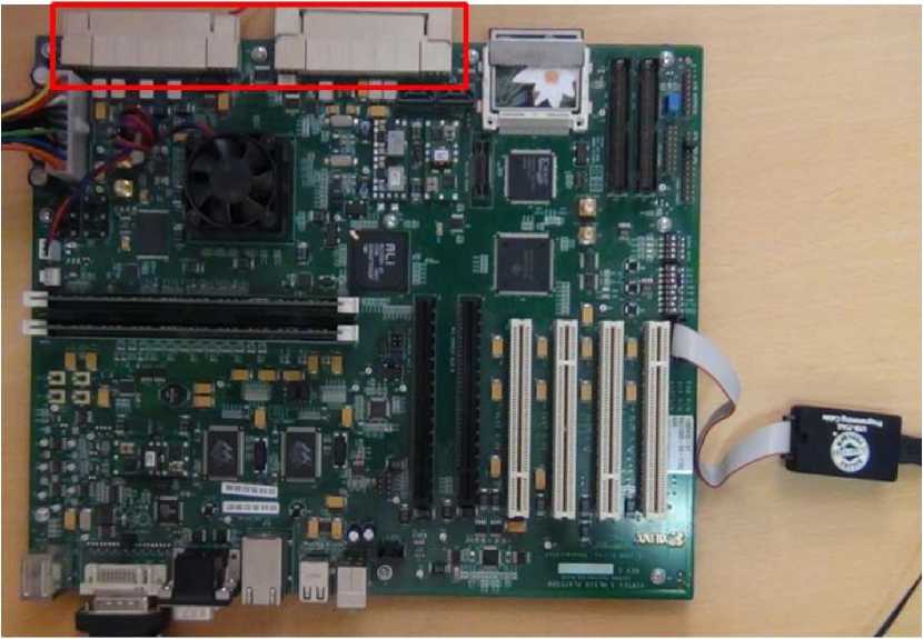
Figure 1. Xilinx ML510 (Virtex-5 FXT) FPGA board
Digilent VDEC1 video decoder board [13], designed using the ADV7183 video decoder chip from analog devices, automatically detects NTSC, PAL, and SECAM video signals (shown in Fig 2.). Automatically detected standard baseband television signals are digitized with ADCs and output data can be sent to a system board. VDEC1 contains all required support circuitry, including well-filtered and stable power supplies, properly terminated 75-ohm inputs, a stable
27-MHz clock source, various video input connectors, and input protection networks. This decoder board has been facilitated with 100-pin Hirose FX2 socket connector for interfacing with a corresponding Hirose plug connector on a system board. To avoid damage and insure proper functioning of VDEC1 video decoder board, it should not be attached to a system board until the signals driving the Hirose connector from the system board have been properly defined.
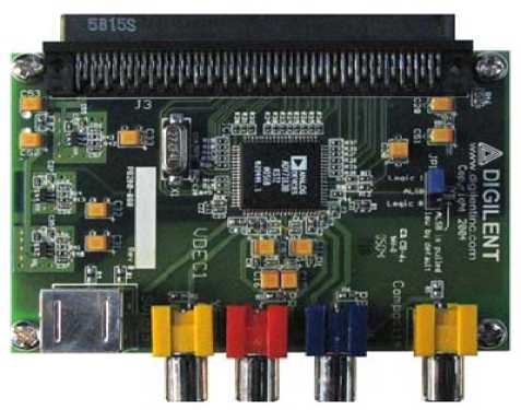
Figure 2. Digilent VDEC1 Video Daughter Card
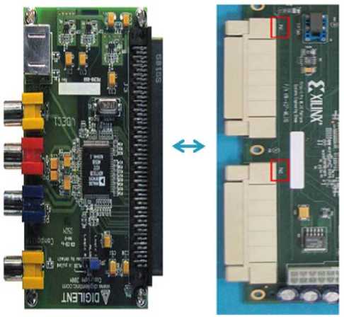
The objective is to connect the video signals coming from Digilent VDEC1 video daughter card with appropriate signal pins on host Xilinx ML510 (Virtex-5 FXT) FPGA board (shown in Fig 3.). For this purpose, we need a PCB having Hirose FX2 connector (for connecting with VDEC1 daughter card) and Tyco Z-Dok+ receptacle connector (for connecting with FPGA board).
The Fig. 4 shows the signal interfacing between Digilent VDEC1 video daughter card and host Xilinx ML510 (Virtex-5 FXT) FPGA board. These signals are: two clocks (LLC1 and LLC2), power down (input to VDEC1 to power up the daughter card), eight bit video data (D0-D7), output enable (OE), Reset (to reset
VDEC1 daughter card), I2C serial data (SDA) and serial clock (SCLK) signals. These signals are 3.3V. Therefore these are connected to FPGA board signals having 3.3V compatibility. The detailed custom PCB layout using Hirose FX2 connector and Tyco Z-Dok+ receptacle connector for interfacing these signals is shown in Fig. 5. Fig.6 shows the ML510 FPGA board with designed camera interface module.
VDEC1
LLC1 PWRDN
LLC2 DO DI D2 D3 OE D4 D5 D6 D7
SCLK SDA RESET
P
C
В
FPGA Board
PM_IO_3V_10_N PM_IO_3V_15_N PM_IO_3V_0_P
PM_IO_23_N PM_IO_3V_11_P PM_IO_3V_17_N
PM_IO_3V_5_P PM_IO_3V_19_N PM_IO_3V_24_P PM_IO_3V_25_N PM_IO_3V_18_P
PM_IO_3V_7_N PM_IO_3V_22_P
PM_IO_3V_9_N PM_IO_3V_13_N
Figure 4. Signal Interfacing between VDEC1 and ML510 FPGA Board
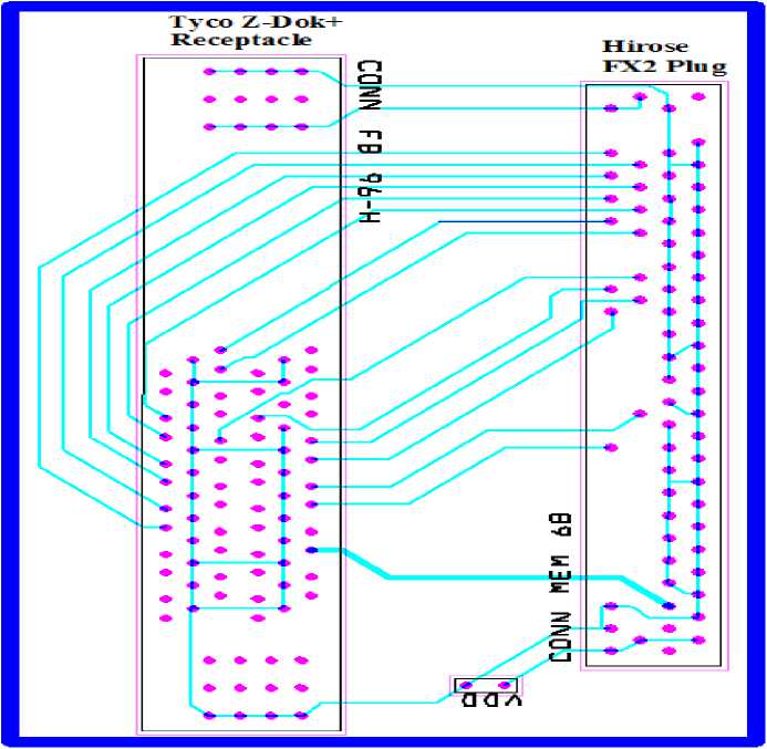
Figure 5. Custom PCB Layout
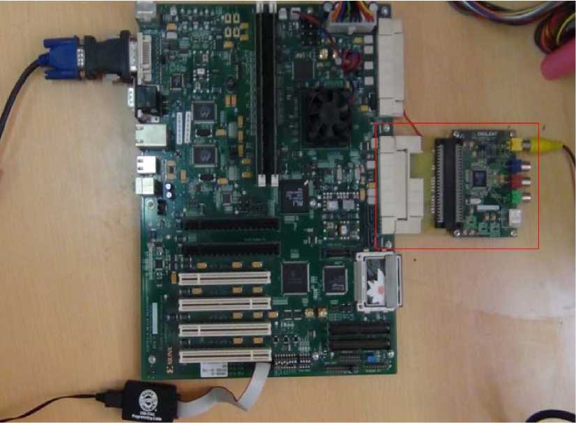
Figure 6. ML510 FPGA Board with Designed Camera Interface
A simplified conceptual block diagram of the whole system is given in Fig. 7 to illustrate the data flow within the system. I2C Master IP is used to program the ADC chip on video daughter card. The two signals used by I2C for programming are serial clock (SCLK) and serial data (SDA). The line field decoder use the digital video signals available at the FPGA interface to produce 4:2:2 format video. Video timing extraction unit takes the inputs from Line Field Decoder and produces the video timing control signals. The video timing signals include Hsync, Vsync, Blank, Hblank, Vblank, Pixel clock (PCLK). The 4:2:2 video is converted into 4:4:4 format by reproducing the color components. YCrCb video is converted into RGB format. RGB data is buffered in two line buffer FIFOs in alternate fashion. Each FIFO stores one line of pixel data. If pixel data is written in FIFO1 RGB then the reading is done from FIFO2 RGB and if data is written in FIFO2 RGB then reading is done from FIFO1 RGB. The switching between two FIFOs is done at the end of each line of image pixel data. Switching between two FIFOs is done by using the multiplexer at the input side and demultiplexer at the output side. The control signals to multiplexer and de-multiplexer decides the operation to be performed for a particular FIFO for reading or writing. The processing block takes the pixel data as input and passes it to DVI Controller. DVI controller is used to display the processed data on display monitor.
-
III. RESULT
The complete analog camera interface module is designed for Xilinx ML510 (Virtex-5 FXT) FPGA board. The interface is capable of capturing real-time video/images. The design is running at 27MHz. It utilizes only 480 out of 81920 slice registers (< 1%), 527 out of 81920 slice LUTs (~ 1%), and 3 (36K) BlockRAMs out of 298 (1%). The synthesis results (Table 2) show that the camera interface module utilizes approximately 1% of the total resources available on Xilinx ML510 (Virtex-5 FXT) FPGA board and therefore enough resources are left for implementation of complex computer vision applications required for automated video surveillance system. Fig. 8 shows realtime video capturing and displaying on monitor through analog camera connected with ML510 FPGA platform.
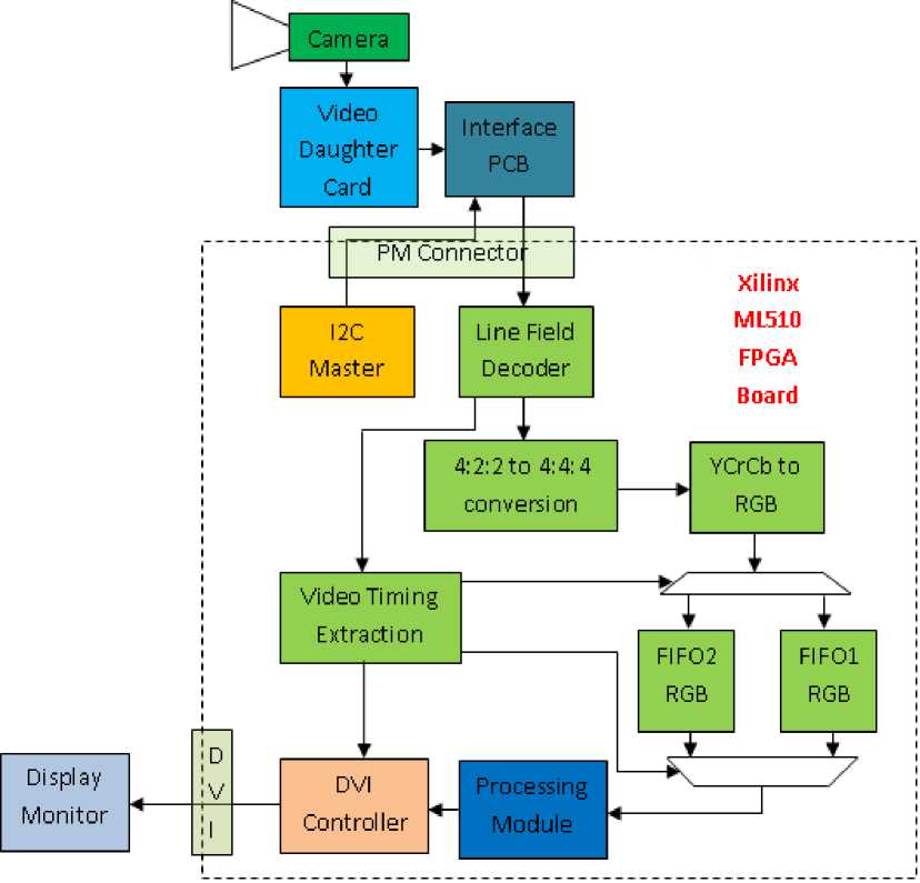
Figure 7. Conceptual Block Diagram of Camera Interface Design
TABLE II. SYNTHESIS RESULTS
|
FPGA Resources |
Utilized |
Total Available |
Percentage |
|
Slice Registers |
480 |
81920 |
< 1% |
|
Slice LUTs |
527 |
81920 |
< 1% |
|
Route-thrus |
84 |
163840 |
< 1% |
|
Occupied Slices |
230 |
20480 |
~ 1% |
|
Block RAMS |
3 (36K) |
298 |
~ 1% |
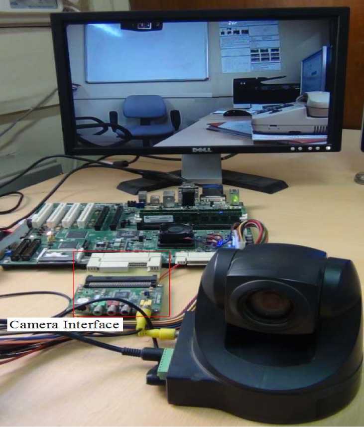
Figure 8. Complete System Setup
-
VI. CONCLUSION
In this paper, the design and implementation of camera interface module required for connecting analog camera with Xilinx ML510 (Virtex–5 FXT) FPGA board is introduced that can robustly capture the images/video from a video camera within real-time constraints. This is an early effort to start the design of a complete FPGA based automated video surveillance system, which can automatically perform the real-time analysis of a scene, monitor a scene, and manage surveillance data. It can be used as a guide for design of camera interface module for any FPGA platform.
ACKNOWLEDGMENT
The authors express their deep sense of gratitude to Dr. Chandra Shekhar, Director CSIR-CEERI for encouraging research and development activities. Authors would like to thanks Dr. AS Mandal, Chief Scientist and Raj Singh, Chief Scientist and Group Leader, IC Design Group, CSIR-CEERI, for their constructive suggestions throughout this work.
References Interfacing the Analog Camera with FPGA Board for Real-time Video Acquisition
- Vega-Rodrı´guez M A, Sa´nchez-Pe´rez J M, and Go´mez-Pulido J A, Recent advances in computer vision and image processing using reconfigurable hardware, Microprocessors and Microsystems, vol. 29, pp. 359-362, 2005.
- Meng H, Pears N E, and Bailey C, FPGA based video processing system for ubiquitous applications, Perspectives in Pervasive Computing, pp. 57-63, 2010.
- Jiang H, Ardo H, and Owell V, A hardware architecture for real-time video segmentation utilizing memory reduction techniques, IEEE Trans. Circuits and Systems for Video Technology, vol. 19, no. 2, pp. 226-236, February 2009.
- Hohnston C T, Gribbon K T, and Bailey D G, Implementing image processing algorithms on PFGAs, Proceedings of the Eleventh Electronics New Zealand Conference ENGCon04, pp. 118 123, 2004.
- Video and Image Processing Design Using FPGAs. White Paper from Altera, 2007.
- Said Y, Saidani T, Smach F, Atri M, and Snoussi H. Embedded Real-time Video Processing System on FPGA. Proceedings of 5th International Conference on Image and Signal Processing. Agadir, Morocco. June 28-30, 2012.
- Zhang B F, Yang Y, Zhu J C, and Li C. Embedded Real-time Image Processing System Based on DM6446+FPGA Architecture. Advanced Engineering Forum, 2012, 6-7: 542-546.
- Said Y, Saidani T, Smach F, and Atri M. Real-time Hardware Co-Simulation of Edge Detection for Video Processing System. Proceedings of 16th IEEE Mediterranean Electrotechnical Conference. Monastir, Tunisia. March 25-28, 2012.
- Hiraiwa J, Vargas E, and Toral S. An FPGA based Embedded Vision System for Real-time Motion Segmenetation. Proceedings of 17th International Conference on Systems, Signals and Image Processing. Brazil. June 17-19, 2010.
- Samanta S, Paik S, Gangopadhyay S, and Chakrabarti A. Processing of Image Data using FPGA-based MicroBlaze Core. Proceedings of International Conference on High Performance Architecture and Grid Computing. Chandigarh, India. July 19-20, 2012.
- Xilinx FPGA Board Data Sheets, (From http://www.xilinx.com/).
- Singh S, Saini A K, Saini R, Mandal AS, Shekhar C, Vohra A, Real-time Video Acquisition and PTZ Camera Movement Control for FPGA based Automated Video Surveillance System, International Journal of Research & Reviews in Computer Science (IJRRCS), vol. 3, no. 2, pp. 1572-1575, 2012.
- Digilent Video Decoder Board (VDEC1) Reference Manual (From www.digilentinc.com) Revision: 4/12/05.
