Low-Cost and Optimized Two Layers Embedded Board Based on ATmega32L Microcontroller and Spartan-3 FPGA

Author: Bahram Rashidi
Journal: International Journal of Modern Education and Computer Science (IJMECS) @ijmecs
Article in issue: 3 vol.5, 2013.
Free access
Microcontrollers and FPGAs both are widely used in digital system design. Microcontroller-based instruments are becoming increasingly widespread. This paper presents design and implementation of a new low-cost and minimum embedded board based on ATMEGA32L AVR microcontroller and Spartan-3 (XCS400-4PQG208C) FPGA in two layers with mount elements on top and button of board. Using of AVR microcontroller in proposed board it adds many features include Analog to Digital Converter (ADC), Digital to Analog Converter (DAC), 32 Kbytes flash memory, 2 Kbytes SRAM, 1024 bytes EEPROM memory. The design goal was to implement as many as possible low-cost and minimum size of the board, also to receive and process input signals in a short time period as real time. The board features are; mount elements in two side of the board for minimization of proposed board and also place decoupling capacitors (by pass) for the FPGA in bottom layer of board strictly below this IC because they should be placed as close as possible to the power supply pins FPGA, use GND polygon layer in total top layer and microcomputer ground for FPGA in bottom layer, use two RS-232 serial port, one VGA connector, PS/2 serial port, and SPI serial port on FPGA, use MT48LC16M16A SDRAM-256MB(4*4MB*16), and XCF02S configuration PROM. Size of the proposed embedded board is 10cm*15cm thus this board was optimized of aspect cost, performance, power, weight, and size.
Embedded System Design, Reconfigurable Architectures, Low-Cost, Microcomputer Ground
Short address: https://sciup.org/15014533
IDR: 15014533
Text of the scientific article Low-Cost and Optimized Two Layers Embedded Board Based on ATmega32L Microcontroller and Spartan-3 FPGA
Published Online April 2013 in MECS DOI: 10.5815/ijmecs.2013.03.08
An embedded system is one with a built-in or embedded processor or computer, typically for carrying out some kind of real-time applications and should have some kind of connection to the outside world. It is the application rather than the hardware itself that defines the embedded system. Embedded Systems have been around since the early days of computers. However, in those days, the number of such systems was not very large basically because of the hardware cost. Although there are infinite varieties of embedded systems, the principles of operation, system components and design methodologies are essentially the same but vary in complexity depending on the application. Based on time constraints, real time systems can be hard real-time which must satisfy deadlines on each and every occasion. With the new advances in embedded systems design, more complex applications may be implemented. During the development of an embedded system certain process models are followed. These models usually include the development of a working prototype of the final system. Embedded systems are single-functioned systems which are tightly constrained by power and cost, and are reactive and real-time [1]. In this paper, we design and implementation a new low-cost and minimum embedded board in two layers based on ATMEGA 32L AVR microcontroller and Spartan-3 FPGA. The proposed board is for implementation of digital signal processing (digital filter design and …) and serial data acquisition and other digital applications. We for select total of elements using optimized elements and with minimum footprint, more elements are SMD until we have better and good electrical characteristics and also have smaller size. In this board FPGA is reprogramming to JTAG emulator. In order to program the microcontroller use USB programmer on board this programmer is based on an ATmega8 AVR microcontroller use USB port for programming the microcontroller is one of benefits proposed embedded board, so it do not need a separate programmer. For FPGA programming in the proposed embedded board we use a XCF02S serial configuration Flash PROM to store FPGA configuration data and potentially additional non-volatile data, including MicroBlaze application code. In order to configure the FPGA from platform flash memory P5 header is used. In recent years, a number of companies have been proposed for Implementation of embedded board by using the FPGA and Microcontroller has been produced by Silica companies [2], this company designed Xynergy board an ARM Cortex-M3 based STMicroelectronics STM32F217 controller with a Xilinx Spartan-6 low-cost FPGA (XC6SLX16) in one design. There are numerous development tools for either ARM Cortex-M microcontrollers or FPGA kits, but this is the first module in the market that merges both technologies on one board, although it is absolutely common to have a microcontroller next to an FPGA, performing tasks that cannot be integrated in the FPGA in a cost-effective way.
High costs for the adequate IP cores and for the additionally needed resources in the FPGA very often require an implementation in favor of a two-chip solution. Particularly the use of standard communication interfaces like Ethernet, USB and CAN are in most cases cheaper and easier to implement on a microcontroller. The remainder of the this chapter is organized as follows: Section II focuses on proposed hardware for the microcontroller AVR and FPGA, description of power supply is proposed in section III, proposed PCB design for the embedded board is in the section IV and in section V comparison and experimentation is proposed and also finally section VI provides the conclusion of this paper.
-
II. Hardware Of Proposed Embedded Board
Microcontroller and FPGA are complementary solutions that provide best-of-both-world processing approaches for high performance real time signal processing systems, and allow designers to capitalize on two complementary technologies where they are best suited. They offer high-speed, real-time processing performance, low unit power consumption and affordable unit prices. Software programmability also makes them very flexible. FPGAs are increasingly used in real time signal processing. They offer very high performance (parallel processing), flexibility through programmable hardware and affordable cost for complementary functions. Complementary solution FPGAs typically complements programmable Microcontrollers in high-performance real-time systems in one or more of the following ways:
-
• Performance acceleration in the signal processing • System logic maxing and consolidation
-
• New peripheral or bus interface implementation
Microcontroller and FPGA are two different methods used for signal processing. Both technologies are good depending on the processing requirement. With the development of Microcontroller and FPGA technology in the recent years, these are more and more applications using of combined Microcontroller and FPGA applied widely in digital applications. Although embedded systems are application specific, some degree of reprogrammability is desired and essential. The reprogrammability assists when upgrading the devices, it is much easier to change the software slightly rather than develop the entire hardware from scratch. In this work, FPGA is used for creating an efficient interface of the sensor with serial data and other peripherals with the Microcontroller, Therefore, two RS-232 ports, and one SPI port are created and connected to the FPGA. So it tends to reduce the number of chips in a compact system.
-
A. Proposed Hardware for The Microcontroller
Microcontrollers are fun. They are the heart and soul of many everyday appliances. And most of all, microcontrollers are easy to use and to design with, from the point of view of a designer. Microcontrollers can interface to motors, a variety of displays as output devices, communicate to PCs, read external sensor values, even connect to a network of similar controllers, and it can do all that without a lot of extra components. This leads to a small and compact system that is more reliable and cost-effective (because of the fewer number of components and the fewer number of interconnections). Its only has a CPU. To build a system to interface to various devices (motors, displays, etc.) would need external program memory and RAM besides the other required peripheral interface components needed to connect the motors, displays, sensors, etc., to the CPU chip. Imagine the number of additional components! Rather than being a single-chip system, you would end up with a system with a board full of components with increased power consumption. Let us look at the various microcontroller components [3].
-
1. CPU: The central processing unit (CPU) is the heart of the controller. It fetches the instructions stored in the program memory, decodes these instructions, and executes them. The CPU itself is composed of registers, the arithmetic logic unit (ALU), instruction decoder, and control circuitry.
-
2. Program Memory: The program memory stores the instructions that form the program. To accommodate larger programs, the program memory may be partitioned as internal program memory and external program memory in some controllers. Program memory is usually nonvolatile and is of EEPROM or EPROM or Flash or Mask ROM or OTP (one-time programmable) type.
-
3. RAM: The RAM is the data memory of the controller, i.e., it is used by the controller to store data. The CPU uses RAM to store variables as well as the stack. The stack is used by the CPU to store return addresses from where to resume execution after it has completed a subroutine or an interrupt call.
-
4. Clock Oscillator: The controller executes the program out of the program memory at a certain rate. This rate is determined by the frequency of the clock oscillator. The clock oscillator could be an internal RC-oscillator or an oscillator with an external timing element, such as a quartz crystal, an LC resonant circuit, or even an RC circuit. As soon as the power is applied to the controller, the oscillator starts operating.
-
5. Reset and Brownout Detector Circuit: The reset circuit in the controller ensures that at startup all the components and control circuits in the controller start at a predefined initial state and all the required registers are initialized properly. The brownout detector is a circuit that monitors the power supply voltage, and if there is a momentary drop in voltage, resets the processor so that the drop in voltage does not corrupt register and memory contents, which could lead to faulty operation of the controller.
-
6. Serial Port: The serial port is a very useful component on the controller. It is used to communicate with external devices on a serial data basis. The serial port can operate at any required data transfer speed. The serial port takes data bytes from the controller and shifts out the data one bit at a time to the output. Similarly, it accepts external data a bit at a time, makes a byte out of 8 such bits, and presents this to the controller. Serial ports are of two types: synchronous and asynchronous. Synchronous data transfer needs an accompanying clock signal with each data bit for timing information, while the asynchronous data transfer does not need the clock signal, and the timing information and synchronization is embedded in the data bit itself by way of duration of data bits as well as additional start- and stop-bits on the data path.
-
7. Digital I/O Port: The microcontroller uses the digital I/O components to exchange digital data with the outside world. Compared to the serial port, which transfers data serially, one bit at a time, the data on the digital I/O port is exchanged as bytes.
-
8. Analog I/O Port: Analog input is performed using an analog-to-digital converter (ADC). The controller could be equipped with an integrated ADC or an analog comparator, which is used under software control to perform A-to-D conversion. ADCs are used to acquire sensor data from devices such as temperature sensors and pressure sensors; such sensors often produce proportional analog voltage data. Analog output is performed using a digital-to-analog converter (DAC). Most controllers are equipped with pulse-width modulators that can be used to get analog voltage with a suitable external RC filter. DACs are used to drive motors, for visual displays (of the older VU meter types), to generate sound or music, etc.
-
9. Timer: The timer is used by the controller to time events; e.g., it may be required to output data to a display at some rate. The timer would be used by the controller to generate that rate. The timer can also be used to count events, external as well as internal. In that case the timer is called a counter.
-
10. Watchdog Timer: A watchdog timer (WDT) is a special timer with a specific function. It is usually used to prevent software crashes. It works as follows: Once armed, the WDT increments an internal counter at some rate. If the user program does not reset the counter, the counter overflows, which is used to reset the controller. The user software is programmed suitably, therefore, frequently enough, to reset the WDT to give a sort of “I am alive” indication. The assumption is that if the user program does not reset the WDT, it has failed in some way and therefore rather than a system crash or unpredictable system performance, it is better to reset the system.
-
11. RTC: A real timer clock (RTC) is a special timer with the task of maintaining time of day, date, etc. It can be used to time-stamp events.
-
B. Features of ATmega 32
The AVR core combines a rich instruction set with 32 general purpose working registers. All the 32 registers are directly connected to the Arithmetic Logic Unit (ALU), allowing two independent registers to be accessed in one single instruction executed in one clock cycle. The resulting architecture is more code efficient while achieving throughputs up to ten times faster than conventional CISC microcontrollers. As explained in [4], The ATmega32 provides the following features: 32K bytes of In-System Programmable Flash Program memory with Read-While-Write capabilities, 1024 bytes EEPROM, 2K byte internal SRAM, 32 general purpose I/O lines, 32 general purpose working registers, On-chip Debugging support and programming, three flexible Timer/Counters with compare modes (two 8-bit and on 16-bit), Internal and External Interrupts, a serial programmable USART, a byte oriented Two-wire Serial Interface, 8-channel, 10-bit ADC with optional differential input stage with programmable gain (TQFP package only), a programmable Watchdog Timer with Internal Oscillator, an SPI serial port, and six software selectable power saving modes. The Idle mode stops the CPU while allowing the USART, Two-wire interface, A/D Converter, SRAM; Timer/Counters, SPI port, and interrupt system to continue functioning. The Powerdown mode saves the register contents but freezes the Oscillator, disabling all other chip functions until the next External Interrupt or Hardware Reset. In Powersave mode, the Asynchronous Timer continues to run, allowing the user to maintain a timer base while the rest of the device is sleeping. The ADC Noise Reduction mode stops the CPU and all I/O modules except Asynchronous Timer and ADC, to minimize switching noise during ADC conversions. In Standby mode, the crystal/resonator Oscillator is running while the rest of the device is sleeping. This allows very fast start-up combined with low-power consumption. In Extended Standby mode, both the main Oscillator and the Asynchronous Timer continue to run. The device is manufactured using Atmel’s high density nonvolatile memory technology. The On chip ISP Flash allows the program memory to be reprogrammed in-system through an SPI serial interface, by a conventional nonvolatile memory programmer, or by an On-chip Boot program running on the AVR core. The boot program can use any interface to download the application program in the Application Flash memory. Software in the Boot Flash section will continue to run while the Application Flash section is updated, providing true Read-While-Write operation. By combining an 8-bit RISC CPU with InSystem Self-Programmable Flash on a monolithic chip and FPGA, the Atmel ATmega32 is a powerful microcontroller that provides a highly-flexible and costeffective solution to many embedded control applications.
Fig.1 shows configuration of ATmega 32L.
PAO(ADCO)
PAI (ADC1)
РАЗ (ADC3) PA4(ADC4) PA5 (ADC5) PA6(ADC6) PA7(ADC7)
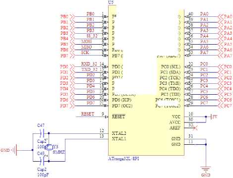
РСЗ (TMS)
PC6 (T06C1)
PC7 (TOSC2)
Fig. 1: Proposed configuration for ATmega 32L microcontroller.
PBO (XCKTO)
PB1 (Tl)
PB2 (AIN0.1NT2)
PB3 (AIN1. OCO)
PB4 (SS)
PB5 (MOSI)
PB6 (b'USO)
(TXD)
PU2 (INTO) PD3 (INTI) PD4(OC1B) PD5 (OC1A)
In recent years presented for AVR microcontroller different programmer, LPT, COM, and USB programmer. As we know ISP programmer using of LPT port, but excessive use of laptops in recent years and given that these systems are not the parallel port thus we use USB programmer on proposed board without need for external programmer. This programmer converts USB to ISP and its interface circuit is one ATmega 8 microcontroller. Schematic of Programmer is shown in Fig. 2.
Fig. 3 shows implemented schematic of USB programmer on board. In proposed design outputs ISP connector is directly connected to ATMEGA32L microcontroller.
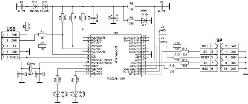
Fig. 2: Schematic of USB programmer on proposed board.
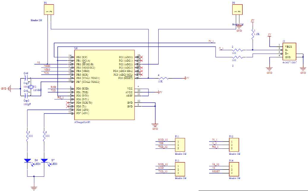
Fig. 3: Implemented schematic of USB programmer on board.
Another element connected to microcontroller is a LCD 16*2. It’s connected to Port C of Atmega 32L. Figure 4 shows P10 connector for placement of LCD. In order to control of brightness LCD we use variable resistant R 1.
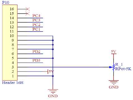
Fig. 4: P10 connector for placement of LCD.
In order to access total of ports microcontroller and to communicate with peripheral device we use four headers 2*4, P4, P5, P6, and P7. Fig. 5 shows these 4 headers.
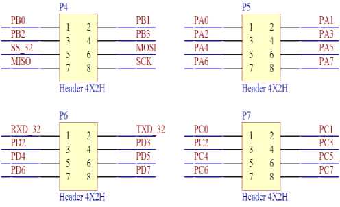
Fig.5: Four headers 2*4, P4, P5, P6, and P7 to access 4 ports of microcontroller.
-
C. Proposed Hardware for The FPGA
In proposed embedded board, a memory is connected to FPGA. This memory is SDRAM (MT48LC16M16A (256MB (4*4MB*16))), in order to storage of data. Data bus between FPGA and SDRAM are 16-bit include address line (A2-A21) and data line (D0-D15). SDRAM is commonly used in applications that require a large amount of memory at fast speeds thus offer the densest and most economical solution for large memory arrays, For example image processing. The disadvantage of SDRAM is the number of control cycles required for operation. The 256Mb SDRAM is a high-speed CMOS, dynamic random-access memory containing 268,435,456 bits. It is internally configured as a quadbank DRAM with a synchronous interface (all signals are registered on the positive edge of the clock signal, CLK). The SDRAM interface is flexible, allowing interfaces to a wide range of SDRAM configurations.
The SDA10 pin has been removed. Address pin EA [5] serves the function of the SDA10 pin for the SDRAM memories. The interface between FPGA and SDRAM allows programming of the addressing characteristics of the SDRAM, including the number of column address bits (page size), row address bits (pages per bank), and banks (maximum number of pages that can be opened), also can interface to any SDRAM that has 8 to 10 column address pins, 11 to 13 row address pins, and two or four banks.
Now based on above description SDRAM connected to FPGA. Fig. 6 shows configuration between SDRAM and FPGA in proposed design.
|
DQ0-DQ15 |
DATA |
PIN2-PIN50 |
|
A0-A12 |
ADDRESS |
PIN2-PIN50 |
|
WE’ CAS’ RAS’ к CS’ о CLK DQML DQMH BA0 BA1 CKE |
TSDWEN |
PIN37 |
|
TSDCASN |
||
|
TSDRASN |
PIN36 |
|
|
TCE0N |
PIN35 PIN78 ^ 0 PIN12 PIN39 to PIN13 PIN34 PIN33 |
|
|
TECLKOUT |
||
|
TBE0N |
||
|
TBE1N |
||
|
TEA15 |
||
|
TEA14 |
||
|
VCC |
Fig. 6: Configuration between SDRAM and FPGA in proposed design.
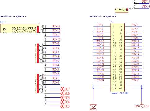
Other elements connect to FPGA are including two RS-232 ports, PS/2 serial port, VGA port, 50Mhz oscillator, two 7-segments, S1 DIP switch, four LEDs, P1 header (20*2), and XCF02S serial configuration Flash PROM to store FPGA configuration data and potentially additional non-volatile data, including MicroBlaze application code by P5 header or JTAG emulator. In this design FPGA play three roles, first role is data acquisition of serial ports and other peripheral interface (P1 header (2*20)). The proposed board provides one expansion connectors for easy interface flexibility to other off-board components. P1 header is connected to BANK1 and BANK2 of FPGA Figure 7 shows this work.
U1A
U1B
Z < a
IO_L01P_0ARN_0
lOATSFOtj— IO_L25N_0 =i^|
IO_L25P_0
IO_L27N_0
IOL30N0

,2 ?v
94___________
.91 P1N35
190 PIN34
VGA_GREEN
VGA_BLUE
UART RXD.2 UART_TXD_2 UART RXD.l 'UART-TXDJ
z < a
IO_L32N_1/GCLK5

LU LJZf L AJULIV-r
IO_L31NJ/VMr_l «i^|-
IO_L31P_1
IO L28N
IO_L28P_1
IOL27N1
82 PIMS
81 PIN27
ISO PIMS
instead use two MAX232s we only using one Max3232, until size of board reduced.
171 PIN21
169 PIN2C
168 PIM 9
” Tv
IO_L10N_1VKEF_1
I0L31NO
XC3S400-4PQG2Q8C
XC3S400-4PQG208C
PIN18
PIM 7 PIMS
P1N33
PIN32
P1N31
PIN30
IO_L10P_lk5^- v 1 лт?ъ 1
IO_L31F_0 4ET_0 =laj Ю152Х 0GC1K7 =3^---
IO_Li2P_0/GCLK6 cl^---2^-
IO L01NJTOJ aS-IO_L01P_1.™ 1|яУ
IO_L01P_2\kN_2
I0/VREF_2
IO_L19P_2
IO L20P 2
IO_L24N_2
IO_L40P_2.VREF_2
IO_L40N_2|-j^
IO_L39N_2|=1K;
IO_L39P_2 -^
Fig.7: Configuration between FPGA and P1 header (2*20).
2 z < a
IO_L19N_2|
Ю_121Р_2|чщ
IO L22N 2
IO_L22P_2 =1^
IO_L23X_2 4er_2
In following we explain configuration between FPGA and others elements:
D. Configuration Between FPGA and Two RS-232 Ports, PS/2 Serial Port:
In proposed embedded board two RS-232 serial ports are connected to FPGA. As shown in Figure 8, the proposed embedded board has two RS-232 serial Ports with male DTE connector based on ICs MAX3232. BANK0 of FPGA related with received signals and transmitted signals of two RS-232 serial Ports. The DCE-style port connects directly to the serial port connector available on most personal computers and workstations via a standard straight-through serial cable. Null modem, gender changers, or crossover cables are not required. Use the DTE-style connector to control other RS-232 peripherals, such as modems or printers, or perform simple loopback testing with the DCE connector. Note that Fig. 6 shows the view looking “out” the DTE connector. Fig. 8 shows the connection between the FPGA and the DB9 connectors in the proposed implementation. The FPGA supplies serial output data using LVTTL or LVCMOS levels to the Maxim device, which in turn, converts the logic value to the appropriate RS-232 voltage level. Likewise, the Maxim device converts the RS-232 serial input data to LVTTL levels for the FPGA. A series resistor between the Maxim output pin and the FPGA’s RXD pin protects against accidental logic conflicts. Hardware flow control is not supported on the connector. The port’s DCD, DTR, and DSR signals connect together, as shown in Fig. 6. Similarly, the port’s RTS and CTS signals connect together. MAX 3232 IC has two MAX232 ICs. Thus
HN25
PIN24
P1N23
PIN22
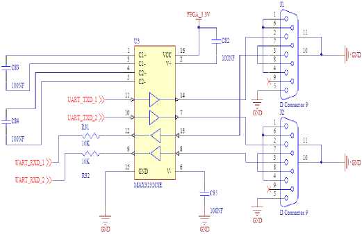
Fig.8: Configuration between two RS-232 serial ports and FPGA based on MAX3232 IC.
TABLE I shows pin connection between RS-232 serial port and FPGA.
TABLE I: PIN CONNECTION BETWEEN RS-232 SERIAL PORT AND FPGA.
|
RS-232 serial port |
FPGA |
|
UART_RXD_2 |
Pin 198 |
|
UART_TXD_2 |
Pin 197 |
|
UART_RXD_2 |
Pin 196 |
|
UART_TXD_2 |
Pin 194 |
Others used serial port in board is PS/2 Fig. 9 shows configuration between PS/2 serial port FPGA
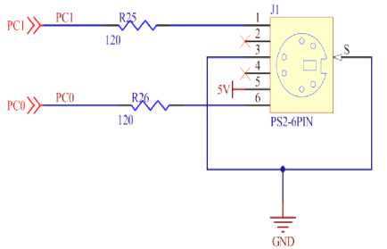
Fig. 9: Configuration between PS/2 serial port and FPGA.
TABLE II shows pin connection between PS/2 serial port and FPGA.
TABLE II: PIN CONNECTION BETWEEN PS/2 SERIAL PORT AND FPGA.
|
PS/2 serial port |
FPGA |
|
PC1(pin1) |
Pin 130 |
|
PC0(pin6) |
Pin 128 |
62 Low-Cost and Optimized Two Layers Embedded Board Based on ATmega32L Microcontroller and Spartan-3 FPGA
E. Configuration Between VGA Port and FPGA
In order to develop of applications proposed board for image and video processing use VGA port on board. Figure 10 shows Configuration between VGA Port and FPGA
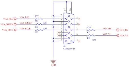
Fig. 10: Configuration between VGA port and FPGA in board.
TABLE III shows pin connection between VGA port and FPGA.
F. Configuration Between 7-segments and FPGA between two
7-
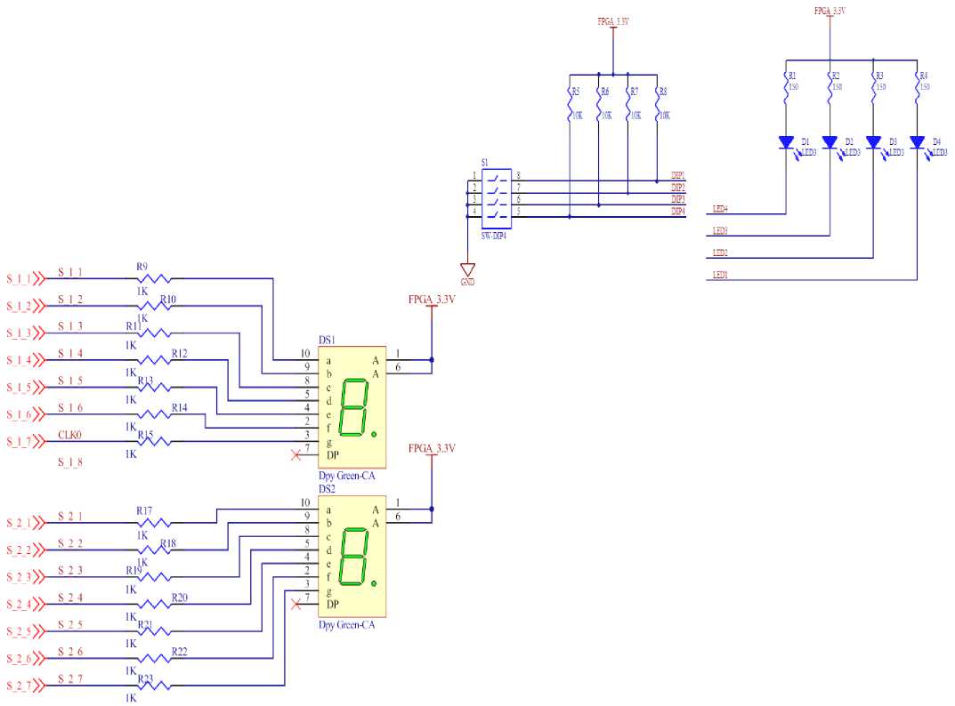
Configuration between oscillator and FPGA is shown in Fig. 13.
Fig.12: Configuration between S1 DIP switch, four LEDs and FPGA in board.
TABLE III: PIN CONNECTION BETWEEN VGA PORT AND FPGA.
|
VGA Port |
FPGA |
|
VGA_RED |
Pin 205 |
|
VGA_GREEN |
Pin 204 |
|
VGA_BLUE |
Pin 203 |
|
VGA_HS |
Pin 200 |
|
VGA_VS |
Pin 199 |
Fig. 11 shows Configuration segements and FPGA on board.
Table IV shows pin connection between two 7-segements and FPGA.
TABLE IV: PIN CONNECTION BETWEEN TWO 7-SEGEMENTS AND FPGA.
|
7-segment 1 |
FPGA |
7-segment 2 |
FPGA |
|
a |
Pin-65 |
a |
Pin-79 |
|
b |
Pin-67 |
b |
Pin-80 |
|
c |
Pin-68 |
c |
Pin-81 |
|
d |
Pin-71 |
d |
Pin-85 |
|
e |
Pin-72 |
e |
Pin-86 |
|
f |
Pin-74 |
f |
Pin-87 |
|
g |
Pin-76 |
g |
Pin-90 |
-
G. Configuration Between DIP switch, 4-LED, and Oscillator with FPGA
In proposed embedded board we use S1 DIP switch and four LEDs for test and control of others components on board. Fig. 12 shows configuration between two 7-segements and FPGA in board
Fig.11: Configuration between two 7-segements and FPGA in board.
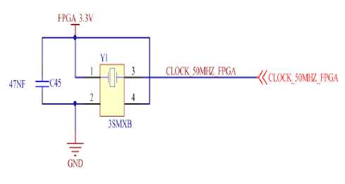
Fig.13: Configuration between oscillator and FPGA.
-
H. Configuration of FPGA and Reading User Data from Configuration PROMs
Figure 14 clearly shows the minimum connections necessary to create a suitable interface between the PROM and the FPGA. This interface allows the FPGA to retrieve data from the PROM before and after configuration and is the simplest implementation for reading user-defined data from a configuration PROM [6]. As explained in [7], After an FPGA is configured, it is often necessary to retrieve user-defined data that is used by the FPGA during operation. The user-defined data needs to be retrieved from an external storage device, requiring an external control circuit to interface to the storage device. This requirement implies additional time for logic design and board level engineering, not to mention extra board real estate requirements and a higher FPGA pin count. Xilinx configuration PROMs are generally used to store an FPGA design, which is downloaded to the FPGA upon system power-up. In most cases, configuration storage is the PROM’s only function, and its capacity is usually not fully used by the FPGA design, leaving the unused portion of the PROM as wasted space.
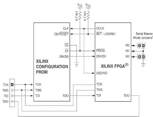
Fig. 14: PROM and FPGA Connections with Additional Control Signal.
Spartan-3 FPGAs are programmed by loading configuration data into robust, reprogrammable, static CMOS Configuration Latches (CCLs) that collectively control all functional elements and routing resources. Before powering on the FPGA, configuration data is stored externally in a prom or some other nonvolatile medium either on or off the board, after applying power, the configuration data is written to the FPGA using any of five different modes: master parallel, slave parallel, master serial, slave serial, and boundary scan (JTAG). The master and slave parallel modes use an 8-bit-wide select map port. Depending on the system design, several configuration modes are supported, selectable via mode pins. The mode pins M0, M1, and M2 are dedicated pins. The mode pin settings are shown in Table V.
TABLE V: SPARTAN-3 CONFIGURATION MODE PIN SETTINGS
|
Configuration mode |
M0 |
M1 |
M2 |
Synchronizing clock |
Data width |
Serial DOUT |
|
Master Serial |
0 |
0 |
0 |
CCLK Output |
1 |
Yes |
|
Slave Serial |
1 |
1 |
1 |
CCLK Input |
1 |
Yes |
|
Master Parallel |
1 |
1 |
0 |
CCLK Output |
8 |
No |
|
Slave Parallel |
0 |
1 |
1 |
CCLK Input |
8 |
No |
|
JTAG |
1 |
0 |
1 |
TCK Input |
1 |
No |
-
I. Configuration Modes
Spartan-3 supports the following five configuration modes:
-
• Slave Serial mode
-
• Master Serial mode
-
• Slave Parallel (Select MAP) mode
-
• Master Parallel (Select MAP) mode
-
• Boundary-Scan (JTAG) mode (IEEE 1532/IEEE 1149.1)
In this design we only using two modes; Master serial mode and Boundary-Scan (JTAG) mode (IEEE 1532/IEEE 1149.1).
-
J. Master Serial Mode:
In Master Serial mode, as explained in [7], the FPGA drives CCLK pin, which behaves as a bidirectional I/O pin. The FPGA in the center of Fig. 15 is set for Master Serial mode and connects to the serial configuration PROM and to the CCLK inputs of any slave FPGAs in a configuration daisy-chain. The master FPGA drives the configuration clock on the CCLK pin to the Xilinx Serial PROM, which, in response, provides bit-serial data to the FPGA’s DIN input. The FPGA accepts this data on each rising CCLK edge. After the master FPGA finishes configuring, it passes data on its DOUT pin to the next FPGA device in a daisy-chain. The DOUT data appears after the falling CCLK clock edge. The Master Serial mode interface is identical to Slave Serial except that an internal oscillator generates the configuration clock (CCLK). A wide range of frequencies can be selected for CCLK, which always starts at a default frequency of 6MHz. Configuration bits then switch CCLK to a higher frequency for the remainder of the configuration.
Fig. 15: Connection Diagram for Master and Slave Serial Configuration
K. Boundary-Scan (JTAG) Mode:
In Boundary-Scan mode, dedicated pins are used for configuring the FPGA. The configuration is done entirely through the IEEE 1149.1 Test Access Port (TAP). FPGA configuration using the Boundary-Scan mode is compatible with the IEEE Std 1149.1-1993 standard and IEEE Std 1532 for In-System Configurable (ISC) devices. Configuration through the boundary-scan port is always available, regardless of the selected configuration mode. In some cases, however, the mode pin setting may affect proper programming of the device due to various interactions. For example, if the mode pins are set to Master Serial or Master Parallel mode, and the associated PROM is already programmed with a valid configuration image, then there is potential for configuration interference between the JTAG and PROM data. Selecting the Boundary-Scan mode disables the other modes and is the most reliable mode when programming via JTAG [7]. We use P6 header (Fig. 16) for select between two mode Master Serial and JTAG mode with one jumper between 2 and 3 pins or 2 and 1 pins. Proposed configuration JTAG connector to FPGA programming is implemented based on P5 header (Fig. 17).
Fig.16: Configuration P6 header for select between two mode Master Serial and JTAG mode.
Fig.17: Configuration JTAG connector to FPGA programming.
Fig. 18 shows proposed implementation for configuration between FPGA and PROM.
Fig. 18: Configuration between FPGA and PROM.
-
III. POWER SUPPLY FOR PROPOSED EMBEDDED BOARd
In this part of paper describes a low-cost power solution for proposed embedded board. In order to maintain high performance and low power consumption a separate core and I/O supply must be supplied to the Spartan-3 XCS400, for the current generation of Spartan-3 XCS400, the supply input for all FPGA I/O banks is 3.3V. The core supply requirement depends on the specific FPGA, and for the current generation of Spartan-3 XCS400 devices is either 1.2V. Voltage 2.5V as VCCAUX (auxiliary voltage) supply input to FPGA. TABLE VI summarizes the voltage supply and consumption requirements for the current of proposed design.
TABLE VI: INPUT AND OUTPUT VOLTAGES AND CURRENTS IN PROPOSED DESIGN
|
Input voltage |
Output voltage |
Output current |
|
V in = 5.5~6v |
V out1 = 3.3v |
I out1 = 1.5A |
|
V in = 5.5~6v |
V out2 = 2.5v |
I out2 = 0.5A |
|
V in = 3.3v |
V out3 = 1.2v |
I out3 = 1A |
We using the FAN1112 1A, 1.2V low dropout linear regulator and the LD1086D2T33 1.5A, 3.3V low drop positive voltage regulator adjustable and fixed, and LD1117 0.5A, 2.5V series low drop fixed and adjustable positive voltage regulators. In continue we explain proposed ICs for considered voltages and currents:
Voltage 1.2V
For product this voltage we use FAN1112 1A, 1.2V low dropout linear regulator The FAN1112 is a 1.2V low dropout three-terminal regulator with 1A output current capability. The device has been optimized for low voltage where transient response and minimum input voltage are critical. Current limit is trimmed to ensure specified output current and controlled shortcircuit current. On-chip thermal limiting provides protection against any combination of overload and ambient temperatures that would create excessive junction temperatures. Unlike PNP type regulators where up to 10% of the output current is wasted as quiescent current, the quiescent current of the FAN1112 flows into the load, increasing efficiency. The FAN1112 regulator is available in the industry-standard SOT-223 and TO-252 (DPAK) power packages. The typical application of this IC is shown in Fig.19.
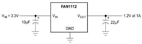
Fig. 19: Typical application of FAN1112 regulator.
Voltage 2.5V
For product this voltage we use LD1117 0.5A, 2.5V series low drop fixed and adjustable positive voltage regulators. The LD1117 is a low drop voltage regulator able to provide up to 800mA of Output Current, available even in adjustable version (V ref =1.25V). Concerning fixed versions are offered the following Output Voltages: 1.2V, 1.8V, 2.5V, 2.85V, 3.0V, 3.3V and 5.0V. We use fixed output voltage 2.5V. Fig. 20 shows Application circuit (for fixed output voltages).
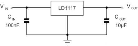
Fig. 20: Application circuit for fixed output voltages of LD1117 regulator.
• Voltage 3.3V
For product this voltage we use LD1086D2T33, 1.5A low drop positive voltage regulator adjustable and fixed The LD1086 is a low drop Voltage Regulator able to provide up to 1.5A of Output Current. Dropout is guaranteed at a maximum of 3.3V at the maximum output current, decreasing at lower loads. The LD1086 is pin to pin compatible with the older 3-terminal adjustable regulators, but has better performances in term of drop and output tolerance. Fig. 21 shows Application circuit of LD1086D2T33 (for fixed output voltages).
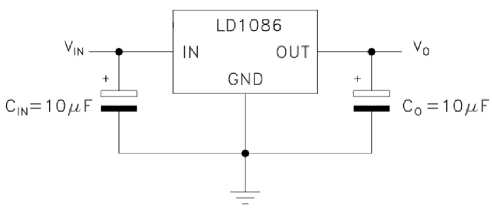
Fig. 21: Application circuit for fixed output voltages of LD1086D2T33 regulator.
-
IV. DESIGN OF PCB PROPOSED EMBEDDED BOARD
For some designers, as explained in [8], the PCB design will be a natural and easy extension of the design process. But for many others the process of designing and laying out a PCB can be a very daunting task. There are even very experienced circuit designers who know very little about PCB design, Proper PCB design is very often an integral part of a design. In many designs (high speed digital, low level analog and RF to name a few) the PCB layout may make or break the operation and electrical performance of the design. It must be remembered that PCB traces have resistance, inductance, and capacitance, just like your circuit does. and as such leave it up to the "expert" specialist PCB designers. Design guidelines to be discussed concern radiofrequency (RF) noise from the microcomputer. This noise is generated inside the device and is coupled out in many different possible ways. The noise is present on all outputs, inputs, power supply, and ground at all times. Potentially, every pin on the microcomputer can be a problem. The biggest problem is noise from the IC input/output (I/O) pins. Because the area covered by traces connected to them on the PCB form a large antenna. These pins also connect to both internal and external cables. The noise from clock switching within the IC appears as ‘‘glitches” on a static output. The glitch is caused by the common impedance of the output pin and the clock drivers, that is, the shared pins that supply each power and ground. The synchronous nature of most devices causes all current-switching events to occur at the same time, making a large noise spike containing RF energy. The second most-important contributor is the power-supply system, which includes the voltage regulation and the bypassing capacitors at both the regulator and at the microcomputer. These circuits are the source of all the RF energy in the system, as they feed the clocked circuits inside the IC with the current required for switching. The third noise source is the oscillator circuit, where the oscillator swings rail to rail. In addition to the fundamental frequency, harmonics are introduced on the output side because the output buffer is digital, which squares the sine wave. Also, any noise caused by internal operations, such as the clock buffers, appears on the output. If proper separation is maintained between the crystal and its tank circuits from other components and traces on the PCB, and the loop areas are kept small, there should be no problems with this noise source. But it has been shown that if ICs or passive components, such as the main VBatt series inductor, are placed close to the crystal, harmonics of the crystal can couple and propagate [8]. We use total of available techniques in different references we try, for decoupling capacitors (bay pass) mount these strictly below the FPGA in bottom layer of board, because they should be placed as close as possible to the power supply pins FPGA. Also oscillators 50MHz placed as close as possible to FPGA.
Microcomputer Grounds
A microcomputer ground is a ground area on the bottom layer underneath the microcomputer that becomes a ground island for the noise made by the microcomputer. This area should extend about 1 / 4 inch outside the outline of the device and tie to the microprocessor ground. Ground connections for the power-supply bypassing capacitors and any bypassing capacitors on the pins also should tie to this ground. Additionally, the ground area should extend out and around the through holes for the oscillator leads and the bypass capacitors tied in to provide the smallest possible loop area when viewed from the Top. See Fig. 22 for an example.
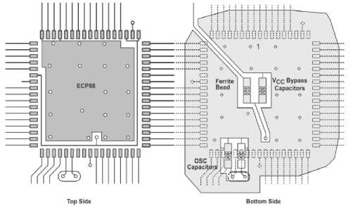
Fig. 22: Microcomputer Ground.
The top side traces are shown in dotted line form on the bottom side diagram for alignment purposes. Notice how the oscillator capacitors lay back over the traces between the device and the crystal. This eliminates loop area. The same is true for the placement of the ferrite bead and Vcc bypass capacitor, being centrally located with the main power lead running almost directly under the lead finger for the ground [9]. Thus we use microcomputer ground in bottom layer strictly below IC FPGA about this IC and decoupling capacitors (by pass) for the FPGA. In Fig. 23 proposed microcomputer ground is shown.
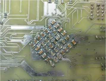
Fig.23: Proposed microcomputer Ground for FPGA about this IC and decoupling capacitors (by pass).
GND Polygon Layer In Total Top Layer
Grounding is fundamental to the operation of many circuits. Good or bad grounding techniques can make or break your design. There are several grounding techniques which are always good practices to incorporate into any design [9].
-
• Use multiple vias to decrease your trace impedance to ground.
-
• “Stitch” required points straight through to your ground plane, don’t use any more track length than you need.
-
• Use copper, and lots of it. The more copper you have in your ground path, the lower the impedance. This is highly desirable for many electrical reasons. Use polygon fills and planes where possible.
-
• Run separate ground paths for critical parts of your circuit, back to the main filter capacitor(s). This is known as “star” grounding, because the ground tracks all run out from a central point, often looking like a star. In fact, try and do this as matter of course, even if your components aren’t critical. Separate ground lines keep current and noise from one component from affecting other components.
We in total of top layer use GND polygon layer until make a good GND chassis for power supply.
Board Zoning
Board zoning has the same basic meaning as board floor planning, which is the process of defining the general location of components on the blank PCB before drawing in any traces. Board zoning goes a little bit further in that it includes the process of placing like functions on a board in the same general area, as opposed to mixing them together. High-speed logic, including micros, is placed close to the power supply, with slower components located farther away, and analog components even farther still. With this arrangement, the high-speed logic has less chance to pollute other signal traces. It is especially important that oscillator tank loops be located away from analog circuits, low-speed signals, and connectors. This applies both to the board, and the space inside the box containing the board. Do not design in cable assemblies that fold over the oscillator or the microcomputer after final assembly, because they can pick up noise and carry it elsewhere [9]. We use board zoning technique for month total elements on proposed board. Real photo of proposed embedded board is shown in Fig. 24.
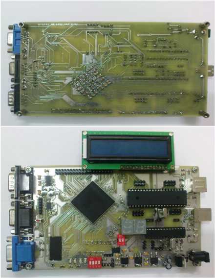
Fig.24: Real photo of bottom and top of the proposed embedded board.
-
V. COMPARISON
Characteristics of embedded systems is that these systems should be capable of real-time processing, have a light weight, have a lower cost, flexibility and ability to be reconfigured, and have convenient and effective communication with peripheral devices. Even though embedded computers have stringent requirements, cost is almost always an issue. We tried as much as possible in the design proposed board made small until to reduce costs. In proposed embedded board has been used of both microcontroller and FPGA technologies so compared to other designs that typically use only one technology microcontroller or FPGA. Other points that have been used in board design include design proposed board based on two layers , unlike commercial available boards that are made in several layers the terms of the construction costs are very expensive the components installed on both sides of the proposed board. The portable system weighing system may become a critical issue therefore we have designed the embedded board with very low weight and perfect for portable systems. Different companies do not report more details of their designed boards. In continue of this section compare different characters of proposed embedded board with other related board. TABLE VII includes compare between main elements in proposed board and [2]. Board [2] using Ethernet, USB, CAN, SPI, I2C connector. But in the proposed board we use two RS232 serial ports, SPI, PS/2, and VGA. Dimension of the proposed embedded board is 10cm*15cm.
TABLE VII: COMPARE BETWEEN MAIN ELEMENTS IN DIFFERENT WORKS
|
45 Й О m |
Й 5 ь О со |
■S ■о Й о я О |
5 о о |
Пн Р-н |
|
[2] |
MT41J64M1 6 1-Gbit DDR3 |
M25P128 SPI NORFlash |
STM32F217 ARM Cortex- M3 MCU |
XC6SLX 16 Spartan-6 |
|
45 V ^ О Й Ни о 2 m Пн |
MT48LC16 M16A 256MB(4*4 MB*16) |
32K bytes of InSystem Programm able Flash |
ATMEGA32L |
Spartan-3, XCS400-4PQG208 C |
-
VI. CONCLUSION
In this paper, a new low-cost and minimum embedded board based on ATMEGA32L microcontroller and Spartan-3 XCS400-4PQG208C FPGA in two layer and mount elements in two side of board for processing different digital algorithm and data a acquisition of sensors with serial port is presented. The aims of the proposed design were developments in low-cost embedded system design, and to explore board-level rapid prototyping using FPGA and microcontroller and also moreover low-cost properties can implement different type’s application on proposed embedded board. In order to meet the requirements of miniaturization, low power of system, all logic control communications and data cache interface circuit have been integrated in FPGA. Approaches, which are using for reduces of size board and cost are including mount elements on two side of board, use ICs with multiple internal module, using simple IC and circuits for power supply, use optimal of total surface board for mount elements as regards board zoning. We test proposed embedded board for different applications to understanding the software and hardware aspects of new low-cost and minimum embedded board, that result have been satisfactory and successfully.
References Low-Cost and Optimized Two Layers Embedded Board Based on ATmega32L Microcontroller and Spartan-3 FPGA
- Bhavya Daya, "Rapid Prototyping Of Embedded Systems Using Field Programmable Gate Arrays", Bachelor Of Science In Electrical Engineering, Spring 2009.
- "Silica Xynergy Board - STM32 meets Spartan-6", http://www.silica.com/product/silica-xynergy-board-stm32-meets-spartan-6.html.
- Dhananjay V. Gadre, "Programming And Customizing The Avr Microcontroller", McGraw-Hill, 2001.
- Datasheet of ATmega 32L, 2011 Atmel Corporation.
- Datasheet of MT48LC16M16A (256MB (4*4MB*16)).
- Application Note: XC18V00, and Platform Flash PROMs; Spartan-II, Spartan-3, Virtex, and Virtex-II FPGA Families, "Reading User Data from Configuration PROMs", XAPP694 (v1.1.1) November 19, 2007.
- "Spartan-3 FPGA Family Data Sheet", DS099 December 4, 2009.
- David L. Jones, "PCB Design Tutorial", June 29th 2004.
- Texas Instruments, "PCB Design Guidelines For Reduced EMI", SZZA009 November 1999.
