Magnetostatic waves in Y 3Fe 5O 12 films on silicon

Author: Khartsev Sergey, Grishin Alex, Manuilov Sergey
Journal: Ученые записки Петрозаводского государственного университета @uchzap-petrsu
Section: Физико-математические науки
Article in issue: 2 (131), 2013.
Free access
Using pulsed laser deposition (PLD) and post-annealing we fabricated polycrystalline yttrium iron garnet films (YIG) on silicon Si(001) substrates. A temperature of 1000 °C and an annealing time of 10 min result the films with low coercivity Hc = 14 Oe and magnetic losses ∆H = 17 Oe accompanied by effective saturation magnetization 4πMf = 1800 Gs. High quality of the YIG films synthesized on Si substrates allowed simple observation of the magnetostatic waves (MSWs) using MSW filter. MSWs spectrums cover 2-5 GHz frequency range and represent magnetostatic surface waves (MSSW) and magnetostatic forward volume waves (MSFVW) geometries. Observations were found to be in the reasonable agreement with qualitative theoretical predictions.
Yttrium-iron-garnet films, magnetostatic waves
Short address: https://sciup.org/14750388
IDR: 14750388 | UDC: 621.318.134,
Text of the scientific article Magnetostatic waves in Y 3Fe 5O 12 films on silicon
INTRODUCTION Considering possible application of YIGs in
Development of the liquid phase epitaxy (LPE) of ferrites opened a new era of planar microwave devises [9]. LPE offered high quality epitaxial films of different thickness and composition. Especially, it provided low loss yttrium iron garnet (YIG) films that found enormous application in microwave electronics [4], [12], [14]. However, high temperature budget of LPE process strongly limits its possible integration with semiconductor platforms such as monolithic microwave integrated circuits (MMICs).
The great development in YIG-semiconductor integration has been done using technique of epitaxial liftoff [2], [11]. Here LPE grown epitaxial YIG film of several μm is cut from the Gd3Ga5O12 (GGG) substrate using ion implantation and subsequently bonded to the semiconductor substrate. This approach allows fabrication of YIG-semiconductor structures with magnetic losses very close to the YIG films on GGG [11]. However, this approach is rather expensive and for some microwave devices (circulators, phase shifters) the polycrystalline YIGs are still very attractive.
During past two decades the techniques of physical vapor deposition has been developed to allow synthesis of epitaxial YIGs at reduced growth temperatures with near LPE films quality [3]. Eventually these methods were also used to probe their potential capability for YIG-semiconductor integration [1], [6], [7], [10], [16].
MMICs we are limited to GaAs and Si. Both of them have strong lattice mismatch with GGG substrates used for epitaxial YIG growth. In contrast to Si, GaAs has better microwave performance but it is expensive and more sensitive to the high temperature budget [12]. Therefore, most of research efforts are focused on the non-epitaxial YIGs synthesis on Si substrates.
Pulse laser deposited YIGs oriented to the microwave applications were firstly reported Karim and Buhay [7], [16]. In work [16] 100 μm thick YIG films were grown on Si substrates. These films had magnetic losses ΔH = 84 Oe and saturation magnetization 4πMs = 1680 Gs and were supposed to be used in high frequency circulators. The further progress in the growth process was made in [10] where lower losses ΔH|| = 73 Oe and higher saturation magnetization 4πMs = 1730 Gs have been achieved. Only recently authors [6] prepared YIG films with just slightly improved ΔH|| = 70 Oe.
Our excessive attempts to grow YIG films onto Si substrates passed through the searching of buffer YIG-Si sublayers (like in [1]) to the direct deposition of YIG onto silicon substrates what yielded surprisingly better quality assessed by ferromagnetic resonance spectroscopy (FMR) and vibrating sample magnetometry (VSM). Taking advantages of the growth technique our integrated YIG-Si samples were found to be very attractive for studying magnetostatic waves (MSWs) guided by YIG semiconductor structures.
FILMS PROCESSING AND PROPERTIES
Yttrium iron garnet films were grown directly onto Si(001) substrates with the resistivity of 3 kΩ × cm. The KrF 248-nm excimer laser was used to ablate overstoichiometric Y3Fe5O12 + 122 % wt. Fe target. The YIG deposition rate was 0,14 Å/pulse at room temperature, 2 mTorr oxygen pressure, laser energy density of 2,5–3 J/cm2, 20 Hz repetition rate, and substrate-to-target distance of 6 cm. Films were post-annealed at 1000 °C in air for 10 min. The main requirement used to optimize processing parameters (oxygen pressure, target-to-substrate distance, and post-annealing conditions) was the achievement of narrow FMR linewidth ∆H .
Synthesized YIGs reveal single Y3Fe5O12 phase polycrystalline films structure without any preferential orientation of crystallites that was verified by X-ray diffraction. The estimated lattice parameter of YIG crystallites a = 12,38 ± 0,02 Å was found using Nelson-Riley function. Within an error its value is coincident with a lattice parameter of bulk Y3Fe5O12 single crystal (12,376 Å).
Differential FMR spectra were recorded in a cavity at the resonance frequency ωexp/2π = 9,1 GHz (TE106 mode). Angular rotation of magnetic field H in the film plane θH = 90° and at the fixed out of plane angle θH = 40° do not reveal any noticeable magnetic anisotropy that agrees to the polycrystalline film structure disclosed by XRD. Fitting of experimental polar angular dependence of the resonance field Hres ( θH ) yields gyromagnetic ratio γ = (1,76 ± 0,01) × 107 rad Gs-1s-1 and effective magnetization 4 πMeff = 1800 ± 20 Gs.
The saturation magnetization 4 πMs = 1630 Gs and coercive field Hc = 14 Oe were measured by VSM for in-plane geometry of external magnetic field H. An observed difference in 4 πMeff and 4 πMs values is on the order of 10 % error for the VSM measurement, but it can be also induced by growth anisotropy on the order of 170 Oe.
For better comparison with other available works on YIG/Si all im-portant data are collected in Table. Here one can see the main advantages and disadvantages of our YIG/Si(001) films.
MAGNETOSTATIC WAVES
To study propagation of magnetostatic waves in the frequency range 2–5 GHz we used 2-port MSW band-pass-filters thoroughly described elsewhere [15]. The filters consist of antennae with 2 mm2 and 0,4 mm2 active areas where MSW excitation transducers widths are w = 240 μm and w = 80 μm, respectively. The MSW travailing distance is also different, it is s ≈ 160 μm for 2 mm2 and s ≈ 60 μm for 0,4 mm2 antennae.
Circular shaped YIG/Si(001) samples entirely cover active area of the filters. The microwave signal at the level of -10 dBm was derived from a HP8722D model vector network analyzer and fed to the microwave cell through the 50 Ω coaxial transmis- sion lines. Network calibration was performed with a samples assembled measurement cell at zero magnetic fields. In 2–5 GHz frequency range this corresponds to the rejection level of 40–31 dB for 2 mm2 and 33–39 dB for 0,4 mm2 antennae. Scattering parameters were recorded averaging 16 consecutive frequency spans.
Progress in the developing of YIG/Si structures.∆H defines peak-to-peak FMR linewidth
|
Ref. |
Deposition method |
Film thickness, μm |
Growth temperature, °C |
Post-annealing temperature, °C |
|
|
[2] |
rf-magnetron sputtering |
1,2 |
RT |
900 |
|
|
[7] |
PLD |
100 |
750 |
850 |
|
|
[8] |
rf-magnetron sputtering |
1,2 |
RT |
900 |
|
|
[9] |
rf-magnetron sputtering |
0,98 |
500 |
750 |
|
|
[10] |
PLD |
0,5 |
850 |
– |
|
|
our |
PLD |
0,96 |
RT |
1000 |
|
|
Annealing time, min |
4 πM s , Gs |
H c , Oe |
∆H || , Oe |
∆H y , Oe |
|
|
[8] |
120 |
1730 |
23 |
70 |
– |
|
[9] |
1/3 |
1680 |
– |
– |
84 |
|
[10] |
120 |
1730 |
9 |
73 |
– |
|
[11] |
5 |
1600÷1710 |
32÷40 |
– |
– |
|
[12] |
– |
1514 |
37 |
180 |
190 |
|
our |
10 |
1630 (1800 – 4 πM eff measured with FMR) |
14 |
56 |
17 |
Figs. 1 and 2 show S 21 and S 11 parameters for YIG(0,96μm)/Si film arranged in MSSW geometry for both antennae types. MSFVW geometry is presented in Fig. 3 for 2 mm2 antenna only. All figures demonstrate common trends, the S1 1 parameter increase with frequency that is a result of better coupling of MSW with rf-field of antenna transducers. This is also a main reason of S 21 increase, especially for 2 mm2 antenna.
An important evidence of MSSW propagation is a moderate decay of the frequency difference δω with increasing magnetic field H (insets to Figs. 1 and 2). Here δω is calculated as difference in experimental maxima/minima of resonant transmission/ reflection ( S 21/ S 11) and uniform FMR frequency that is given for two different geometries as follows:
tores = YH (H + 4nM efr) in — plane H, tores = /(H - 4nMerr) perpendicular H.
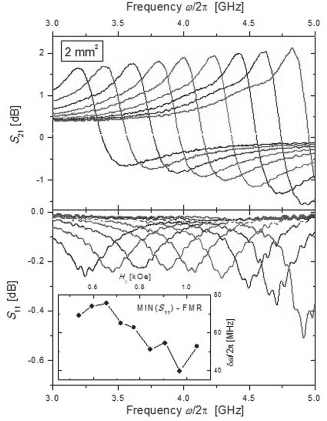
Fig. 1. Transmission characteristics of magnetostatic surface waves (MSSWs) in YIG(0,96μm)/Si(001) film recoded for filter with 2 mm2 antenna. Magnetic field H is swept from 538 to 1044 Oe. Inset shows H -dependence of the frequency difference δω between uniform FMR mode and minimum of S 11 parameter
It is also worse to mention that for both geometries (MSSW and MSFVW) δω is computed taking into account experimental errors Δγ and Δ4 πMeff , and represents the possible lowest value.
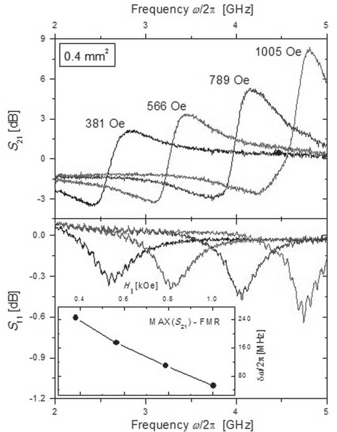
Fig. 2. Transmission characteristics of magnetostatic surface waves (MSSWs) in YIG(0,96μm)/Si(001) film recoded for filter with 0,4 mm2 antenna. Inset shows H -dependence of the frequency difference δω between uniform FMR mode and maximum of S 21 parameter
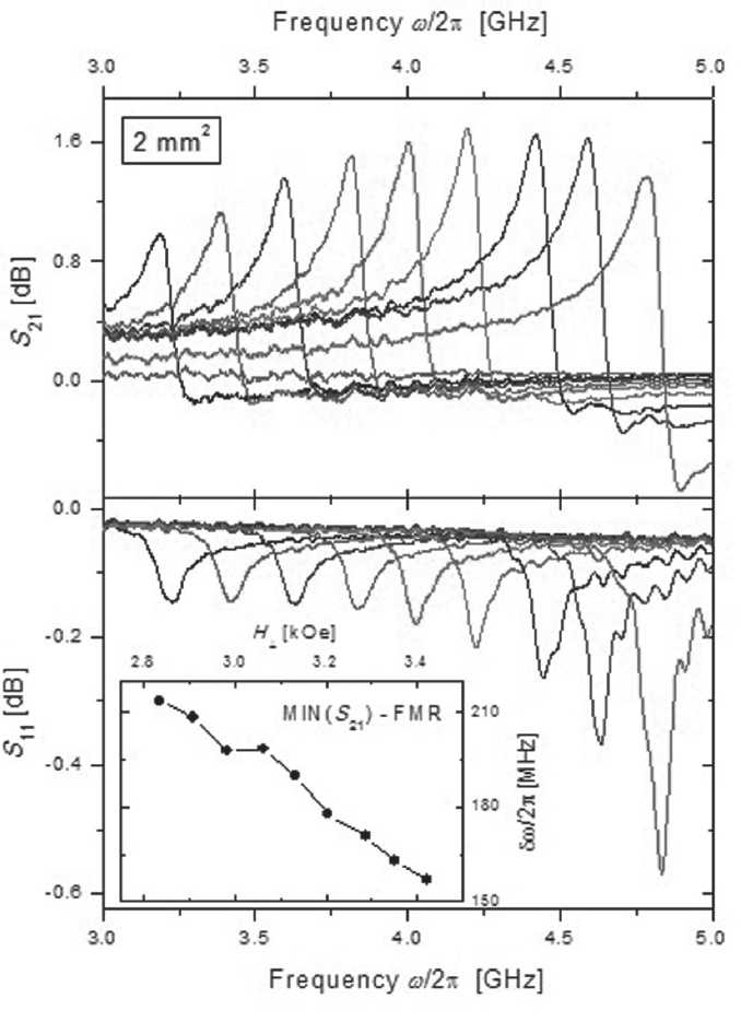
Fig. 3. Transmission characteristics of magnetostatic surface waves (MSFVWs) in YIG(0,96μm)/Si(001) film recoded using filter with 2 mm2 antenna. Magnetic field H is swept from 2835 to 3422 Oe. Inset shows dependence of S21 minimum on external magnetic field H . Solid lines are uniform FMR modes calculated for perpendicular geometry taking into account Δγ and Δ4 πMeff errors
As one can see, our observations qualitatively coincide with theory. Fig. 4 shows MSSW and MSFWV dispersion relations calculated for our lossy 0,96 μm-thick YIG film. The calculations have been done using simplified equations for wave vector k from [14]
_£lnГ Д - Д + Д + Д 2 d _ Д 2 - Д 2 - Д 1 + LU
– MSSW
k = — tan 1 в
- в Д 1
– MSFVW
where д = 1 +
to o ^ M = toto M
, в = ^ — Д 1 with
2 2 , Д 2 2 2
to o — to to o — to
ω = γH , ω = γ 4 πM and d as a film thickness. The
0 M eff magnetic losses were introduced in dispersion relations by substituting ω0 → ω0+ iαω [5]. The damping parameter α we roughly estimated from FMR line widths for parallel and perpendicular geometries a = yAH(||±)to/2toexp [5], toexp/^^n = 9,1 GHz.
MSSW dispersion curves clearly demonstrate shrinking of MSSW propagation band what we ob- serve in Figs. 1 and 2 (insets) through the reduction of δω while increasing magnetic field H. The strong deviations of δω in Fig. 1 result from lower signal to noise ratio for S11 parameter. Also, mention that higher values of δω for 0,4 mm2 antenna (inset to Fig. 2) nicely correlate with calculations in Fig. 4(a), see variation of MSSW bandwidth at k = 131 cm-1 and k = 393 cm-1, correspondingly for 2 mm2 and 0,4 mm2 antennae. The vivid difference in the structure of MSSW spectrums (Figs. 1 and 2) we rely on the different coupling of MSSWs with rf-field of microstripe transducers for 2 mm2 and 0,4 mm2 antennae.
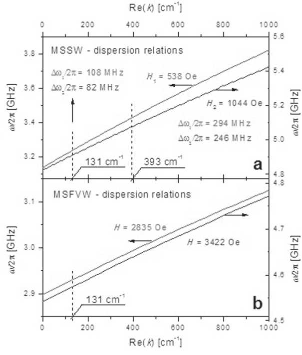
Fig. 4. Computed MSSW and MSFVW dispersion curves
In the case of MSFVW geometry, calculations have resulted in almost constant ”bandwidth” δω of MSFVWs propagation for the studied range of magnetic fields H, that is shown in Fig. 4(b). Taking wave vector k = 131 cm-1 we get δω = 31 MHz. However, we observe clear contradiction with experimental data given in Fig. 3 (inset), where δω constantly decays starting from 214 MHz at H = 2835 Oe down to 157 MHz at H = 3422 Oe. This strong dependence of δω on magnetic field H we mostly rely on approximately 5° misalignment of magnetic field vector H with the film normal during MSFVWs measurements.
Qualitatively good correlation with theory appears in the observed difference of MSWs bands for MSFVW and MSSW geometries. Calculations in Fig. 4 predict lower frequency band for MSFVW what we easily see in S 11 and S 21 spectrums of Figs. 1 and 2. Moreover, Figs. 1 and 2 demonstrate increase of the frequency bands of MSSWs while changing from 2 mm2 to 0,4 mm2 antenna. This is a result of the higher range of exited wave vectors k for 0,4 mm2 antenna (see Fig. 4 (b)).
We also estimated MSWs propagation losses using simple equation L p(dB) = 20 log[exp(Im( k ) s )] where imaginary part of the k -vector is computed using dispersion relations for MSSW and MSFVW. In the case of MSSW, when magnetic field H is swept from 538 Oe to 1044 Oe we found the losses ranged as follow: L p = 12÷18 dB at k = 131 cm-1 and L p = 5÷8 dB at k = 393 cm-1. For MSFVW geometry H is swept from 2835 Oe to 3422 Oe what yields to L p = 8÷12 dB at k = 131 cm-1. And the total losses can be approximated as Lt = I - L p + log[1 - 10 ( 5 11 /10)] | Taking experimental values for reflection S 11 parameter of MSSWs we get L t = 42 dB at H = 538 Oe and L t = 41 dB at H = 1044 Oe for 2 mm2 antenna, while for 0,4 mm2 antenna we have L t = 31 dB at H = 538 Oe and L t = 29 dB at H = 1044t Oe. The total losses for MSFVW geometry are L t = 42 dB at H = 2835 Oe and L t = 33 dB at H = 1t044 Oe. As one can see, our YIG-Si based filters represent good agreement between total losses L t and transmission losses defined by filter rejection levels (given earlier) and measured S 21 parameters of MSW assisted propagation (Figs. 1–3).
CONCLUSIONS
We grew polycrystalline YIG/Si(001) films with remarkable properties. The films possess better magnetic losses A H , high effective magnetization 4nM ef , and have reasonably lowered coercivity H c .
Neglecting certain achievements in the growth process, A H values are still too high for application in the traditional YIG-oriented spinwave electronics. However, current work demonstrates an ability of the YIG-semiconductor structures to conduct MSWs.
* This work was supported by the Vetenskapsrådet (Swedish Research Council), Strategic Development Program of Petrozavodsk State University (2012–2016), Ministry of Education and Science of Russian Federation “Scientific and Educational Community of Innovation Russia (2009-2013)” Program through contracts № 14.740.11.0895, № 14.740.11.0137, № 14.740.11.1157, № 16.740.11.0562, №14.B37.21.0755, № 14.B37.21.0747, № 14.B37.21.1066 and “Development of Scientific Potential of High School” Program № 2.3282.2011 and № 2.2774.2011.
MAGNETOSTATIC WAVES IN Y3Fе5012 FILMS ON SILICON
Using pulsed laser deposition (PLD) and post-annealing we fabricated polycrystalline yttrium iron garnet films (YIG) on silicon Si(001) substrates. A temperature of 1000 °C and an annealing time of 10 min result the films with low coercivity Hc = 14 Oe and magnetic losses ΔH = 17 Oe accompanied by effective saturation magnetization 4 πMeff = 1800 Gs. High quality of the YIG films synthesized on Si substrates allowed simple observation of the magnetostatic waves (MSWs) using MSW filter. MSWs spectrums cover 2–5 GHz frequency range and represent magnetostatic surface waves (MSSW) and magnetostatic forward volume waves (MSFVW) geometries. Observations were found to be in the reasonable agreement with qualitative theoretical predictions.
References Magnetostatic waves in Y 3Fe 5O 12 films on silicon
- Effect of CeO2 buffer layer on the microstructure and magnetic properties of yttrium iron garnet fi lm on Si substrate/Q.-H. Yang, H.-W. Zhang, Q.-Y. Wen et al.//J. Appl. Phys. 2009. Vol. 105. P. 07A507-1-07A507-3.
- Epitaxial liftoff of thin oxide layers: Yttrium iron garnets onto GaAs/M. Levy, R. M. Osgood, A. Kumar et al.//Appl. Phys. Lett. 1997. Vol. 71. P. 2617-2619.
- Epitaxial yttrium iron garnet fi lms grown by pulsed laser deposition/P. C. Dorsey, S. E. Bushnell, R. G. Seed et al.//J. Appl. Phys. 1993. Vol. 74. P. 1242-1246.
- Ferrite devices and materials/J. D. Adam, L. E. Davis, G. E. Dionne et al.//IEEE Trans. Microwave Theory Tech. 2002. Vol. 50. Is. 3. P. 721-737.
- Gurevich A. G. Magnetization Oscillations and Waves/A. G. Gurevich, G. A. Melkov. Boca Raton: CRC Press, 1996. 445 P.
- Kang Y.-M. FMR linewidths of YIG films fabricated by ex situ post-annealing of amor-phous films deposited by rf magnetron sputtering/Y-M. Kang, A. N. Ulyanov, S.-I. Yoo//Phys. Stat. Sol. A. 2007. Vol. 204. Is. 3. P. 763-767.
- Karim R. Laser ablation deposition of YIG films on semiconductor and amorphous substrates/R. Karim, S. A. Oliver, C. Vittoria//IEEE Trans. Magn. 1995. Vol. 31. Is. 6, part 2. P. 3485-3487.
- Kawasaki K. The Interaction of Surface Magnetostatic Waves with Drifting Carriers in Semiconductors/K. Kawasaki, H. Takagi, M. Umeno//IEEE Trans. Microwave Theory Tech. 1974. Vol. 22. Is. 22. P. 918-924.
- Linares R. C. Epitaxial growth of narrow linewidth Yttrium Iron garnet films//J. Cryst. Growth. 1968. Vol. 3. P. 443-446.
- Magnetic properties of YIG (Y3Fe5O12) thin films prepared by the post-annealing of amorphous films deposited by rf-magnetron sputtering/Y.-M. Kang, S.-H. Wee, S.-I. Baik, S.-G. Min et al.//J. Appl. Phys. 2005. Vol. 97. P. 10A319-1-10A319-3.
- Magnetization and FMR studies of crystal-ion-sliced narrow linewidth gallium-doped yttrium iron garnet/F. J. Rachford, M. Levy, R. M. Osgood, A. Kumar et al.//J. Appl. Phys. 2000. Vol. 87. P. 6253-6255.
- Microwave magnetic film devices/D. B. Chrisey, P. C. Dorsey, J. D. Adam et al.//Thin Film. 2001. Vol. 28. P. 319-374.
- Parekh J. P. Propagation characteristics of magnetostatic waves/J. P. Parekh, K. W. Chang, H. S. Tuan//Circuits Systems Signal Process. 1985. Vol. 4. P. 9-39.
- Recent advances in processing and applications of microwave ferrites/V. G. Harris, A. Geiler, Y. Chen et al.//J. Magn. Magn. Mater. 2009. Vol. 321. Is. 14. P. 2035-2047.
- Submicron Y3Fe5O12 Film Magnetostatic Wave Band Pass Filters/S. A. Manuilov, R. Fors, S. I. Khartsev et al.//J. Appl. Phys. 2009. Vol. 105. P. 033917-1-033917-9.
- Thick yttrium-iron-garnet (YIG) films produced by pulsed laser deposition (PLD) for integration applications/H. Buhay, J. D. Adam, M. R. Daniel et al.//IEEE Trans. Magn. 1995. Vol. 31. Is. 6, part 2. P. 3832-3834.
