Mathematical model for contact resistance of cold contact at spot welding

Author: Mishurenko A.B., Kozlovsky S.N.
Journal: Сибирский аэрокосмический журнал @vestnik-sibsau
Section: Математика, механика, информатика
Article in issue: 7 (33), 2010.
Free access
The paper is devoted to the problem of optimizing spot welding modes and contains the description of a mathematical model for the calculation of cold contact initial resistance.
Spot welding, resistance of cold contact
Short address: https://sciup.org/148176482
IDR: 148176482
Text of the scientific article Mathematical model for contact resistance of cold contact at spot welding
The practice of spot welding and the numerous results of published researches unambiguously confirm that one of main conditions of forming quality-welded joints is the optimality of the initial resistance of part -to- part r КТ contact. Its value and stability essentially influences the sizes of a kernel, the stability of the process against creating splashes and poor penetration. At the same time, until now, the development of spot welding technologies of r КТ value had been achieved experimentally for each particular welding condition; this is rather laborintensive.
According to the conducted research it has been concluded that the rod model is the most acceptable engineering technique among all known methods applied in rough surface models for welded contacts; mainly because it describes the mechanism of contact interaction between two rough surfaces with more simplicity and precision (fig. 1).
According to the accepted model of two rough surface contacts, the conductivity in the contact layer is carried out according to n r number of individually parallel micro conductors of d ( d →0) diameter, and of a length, formed by deformable rods (micro lugs). One of the constituents of the total electric resistance in such a micro contact r КТ which is caused by the resistance of micro conductors in the contact layer, which has properties different to those of parent metal, is called the internal contact resistance r КВ . The other part, which is formed by current line curvatures j in near contact areas where properties of the parent metal are assumed to not change, is called the micro geometrical contact resistance r МГ . Then the total electric resistance contact will be equal to the sum of these two components:
r КТ = r КТ + r КТ .
The total internal electric contact resistance r ВН can be defined in the following manner:
ra
ВН = ВН = ρΔ = ρΔ nr nr Δ S
2 A '. '' - 6)
Ar
.
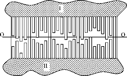
Fig. 1. Contact of two rough surfaces. The rod model
For the accepted model, the micro geometrical resistance for individual contact r * МГ can be defined according to the familiar dependence, considering its presence in two parts (fig. 2):
f 1_1 1 ГМГ = 2p II
V d D )
The total micro geometrical contact resistivity r МГ can be defined accepting the following dependence:
_ ГМГ _ 2p f
ГМГ nr nr V d D)
To calculate r ВН and r МГ it is necessary to define the mechanical parameters of the welded contact and first of all, define the deformation the micro lugs undergo:
whether they are elastic or plastic. This may be done by comparing the pressure σСР operating the in contact outline area, and the critical pressure σ К at which the contact transforms to a plastic state.
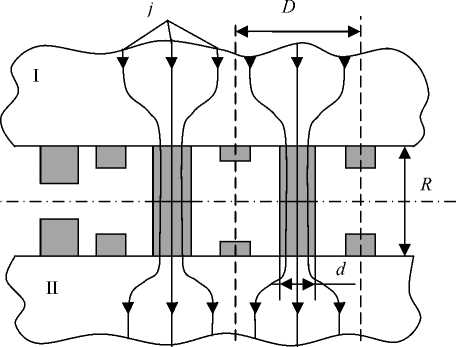
Fig. 2. Contact conductivity in the rod model
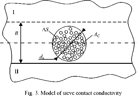
The comparison of σСР and σК values at static electrode force defined by the practice of spot welding modes for parts with a thickness of 0.5–4 mm for various steels and alloys shows that the micro roughness in the welded contacts always deforms plastically. For example, at a change R max within 2.4–37 µm the values σ К / σ 02 and σ СР / σ 02 (in brackets) at spot welding of parts with a thickness of 0.5–4 mm made of 08 and 12Х18Р10Е type steels, and a АМг6 alloy change within: 2·10–6–0,03 (1.6–1.9), 1,2·10–5–0.02 (1.8–2.7) и 2.5·10–5–0.4 (1.8–2.9) accordingly. For comparing plastic and elastic contacts the problem of its mechanical parameter definition is considerably simplified; the actual area of the contact depends only on surface’s micro geometry, and the rapprochement depends only on the material distribution within the rough layer (fig. 3). For these conditions, value ε can be defined applying the dependence:
v σ
СР ε,
I Cs ■ ^02 ■ b J where Cε is the factor considering the metal hardening in micro roughness at its plastic deformation; b, v are the parameters of a basic curve b1, v1 that are defined by the contacting of two equally rough surfaces according to the formula:
b = k ■ 2 v 1 ■ b. 2 , v = 2 ■ v, .
v 12 1 , 1
The number of micro contacts n r and their average diameter d can be defined from the following ratio:
n = A_=AC * n r ΔS 2π Θε , d=

= 22Θ ε.
R мкОм
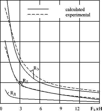
Fig. 4. Results of experimental and calculated resistance values
The average value of the current line spread area from an individual micro conductor can be defined as the area of contacting micro roughness to a number of micro contacts:
ΔAС =AС nr and its diameter d according to the following dependence:
D=

= 2 2Θ ε η
.
Using the results of the researches, studying contact resistance and carrying out reasonable calculations, we have obtained a dependence to calculate the resistance of the welded contact (fig. 4):
r КТ = ρΔ
'^ Rmax ( 1 - в Г
+ ρ
F Э η
πσСР 2Θ ε 2 F Эη
( 1 - vn) .
To define it we need to experimentally measure the value rКТ at any FЭ (it is best to measure rКТ at FЭ as closely to the recommended spot welding area as possible), and then to calculate value pA according to the following dependence:
P a
Fn x
'^ R max ( 1 - £ )
x
r KT - p
ЛОС р
V20 £
2 Fn
( 1 - ^ )
The developed mathematical model describes, with sufficient accuracy, the action of electric resistance in part-to-part contact, which is testified by experimental and calculated values of this resistivity [1–4].
